EP0709762A2 - Dispositif d'entrée à panneau de contact avec une opération d'échantillonnage intermittente - Google Patents
Dispositif d'entrée à panneau de contact avec une opération d'échantillonnage intermittente Download PDFInfo
- Publication number
- EP0709762A2 EP0709762A2 EP95109263A EP95109263A EP0709762A2 EP 0709762 A2 EP0709762 A2 EP 0709762A2 EP 95109263 A EP95109263 A EP 95109263A EP 95109263 A EP95109263 A EP 95109263A EP 0709762 A2 EP0709762 A2 EP 0709762A2
- Authority
- EP
- European Patent Office
- Prior art keywords
- touch panel
- power
- signal
- voltage
- sampling
- Prior art date
- Legal status (The legal status is an assumption and is not a legal conclusion. Google has not performed a legal analysis and makes no representation as to the accuracy of the status listed.)
- Granted
Links
Images


Classifications
-
- G—PHYSICS
- G06—COMPUTING OR CALCULATING; COUNTING
- G06F—ELECTRIC DIGITAL DATA PROCESSING
- G06F3/00—Input arrangements for transferring data to be processed into a form capable of being handled by the computer; Output arrangements for transferring data from processing unit to output unit, e.g. interface arrangements
- G06F3/01—Input arrangements or combined input and output arrangements for interaction between user and computer
- G06F3/03—Arrangements for converting the position or the displacement of a member into a coded form
- G06F3/041—Digitisers, e.g. for touch screens or touch pads, characterised by the transducing means
- G06F3/045—Digitisers, e.g. for touch screens or touch pads, characterised by the transducing means using resistive elements, e.g. a single continuous surface or two parallel surfaces put in contact
Definitions
- the present invention relates to a touch panel input apparatus for inputting characters or the like with a touch panel constituted of electrode panels each composed of a transparent analog resistance film.
- Figs. 18A, 18B and 19 show a prior art touch panel input apparatus (e.g., Japanese Laid-Open patent Publication No. 5-127827).
- an X-direction electrode panel 1 and a Y-direction electrode panel 2 each formed of a transparent electrode are laminated on a display screen such as a liquid crystal display panel or a CRT (cathode ray tube) and bonded to each other.
- a power source Vcc is alternately connected with an end of the X-direction electrode panel 1 and that of the Y-direction electrode panel 2 to generate a voltage distribution in the X-direction and the Y-direction.
- the X-direction electrode panel 1 and the Y-direction electrode panel 2 are brought into contact with each other at a point thereof by pressing the point with a pen or a finger. The coordinates of the pressed point is detected based on the voltage at the contact point.
- one electrode panel for example, the Y-direction electrode panel 2
- Vcc positive power source
- the other electrode panel for example, the X-direction electrode panel 1
- R negative power source
- a voltage (input signal TABIN) which appears on the output resistor R when both the X-direction electrode panel 1 and the Y-direction electrode panel 2 have been brought into contact with each other is detected.
- an operation of turning on the power source is started.
- the conventional touch panel input apparatus has, however, problems as described below:
- the present invention has been developed with a view to substantially solving the above-described disadvantages and has for a first object to provide an improved touch panel input apparatus which can reduce consumption of electricity by preventing leakage between opposed X and Y electrode panels and/or an unnecessary sampling operation from occurring.
- the present invention provides a touch panel input apparatus comprising: a touch panel consisting of two electrode panels one of which has a resistance distribution uniform in an X-direction and the other of which has a resistance distribution uniform in a Y-direction; a touch panel control circuit for, in a power-on state of the apparatus, alternately applying to the two electrode panels a voltage for generating a voltage distribution therein, and detecting a position voltage generated in the electrode panel to which the voltage is not applied when the two electrode panels are brought into contact with each other at a point thereof; and in a power-off state of the apparatus, connecting one end of one of the two electrode panels with a power source and at the same time, grounding one end of the other electrode panel via an output resistor, and sampling a voltage which is developed between both terminals of the output resistor when the two electrode panels have been brought into contact with each other; a contact coordinate calculation means for, in the power-on state, calculating coordinates of a contact position on the touch panel,
- one end of one of the two electrode panels (X-direction and Y-direction electrode panels) composing the touch panel is intermittently connected with the power source, synchronously with the clock signal and at the same time, one end of the other electrode panel is intermittently grounded via the output resistor.
- the sampling means samples a voltage which has appeared at both ends or terminals, of the output resistor, synchronously with the clock signal, when both electrode panels have been brought into contact with each other, and outputs a signal indicating whether or not the sampled voltage is higher than a predetermined level.
- the power-on means executes a power-on operation, based on the signal supplied thereto from the sampling means as the power-on instruction signal.
- the sampling period is long, a voltage is not applied to the touch panel without cease and no leakage occurs between the X-direction and Y-direction electrode panels. Further, electric current is less consumed for a sampling operation than before. That is, the battery has a longer life than before.
- the touch panel control circuit further comprises a sampling stop means for stopping a sampling operation of the sampling means when the signal received from the sampling means indicates that the sampled voltage is equal to or higher than the predetermined level; and the sampling means has a signal holding means for holding the signal outputted from the sampling means.
- the sampling means of the touch panel control circuit samples the voltage which appears on both ends of the output resistor, and outputs the signal indicating whether or not the sampled voltage is equal to or higher than the predetermined level.
- the signal holding means holds the signal outputted from the sampling means.
- the sampling stop means of the touch panel control circuit stops the sampling operation of the sampling means when the sampled voltage is equal to or higher than the predetermined level.
- the signal holding means holds the signal indicating that the sampled voltage is equal to or higher than the predetermined level and the sampling stop means stops the sampling operation of the sampling means.
- the apparatus does not perform the sampling operation after the power-on instruction signal has been outputted.
- electric current is consumed in a less quantity.
- the sampling means outputs the power-on instruction signal to the power-on means for a long time thanks to the signal holding means.
- the power-on operation can be reliably executed even though the touch panel is touched only for a short time period.
- the touch panel control circuit comprises: an input buffer having an input inhibit mode, the voltage developed between the terminals of the output resistor being supplied to the sampling means through the input buffer; and a buffer control circuit for controlling the input buffer such that the input buffer goes into the input inhibit mode when the sampling is not performed.
- the through-electric current does not flow through the input buffer, even when the voltage generated between both ends of the output resistor becomes an intermediate potential between the supply voltage and the ground voltage.
- the touch panel control circuit comprises: a first latch circuit for latching and outputting to the power-on means the signal outputted from the sampling means; a second latch circuit for latching the signal outputted from the sampling means; and a latching operation control means for controlling the first and second latch circuits based on the signal latched by the second latch circuit such that the first latch circuit stops a latching operation when the sampled voltage is equal to or higher than the predetermined level and that the first latch circuit starts a latching operation and the second latch circuit stops a latching operation when the sampled voltage is lower than the predetermined level.
- the second latch circuit of the touch panel control circuit latches the signal outputted from the sampling means. Then, at the start time of the sampling operation, the latching operation control means stops the latching operation of the first latch circuit when it is detected that the sampled voltage is equal to or higher than the predetermined level, based on the signal latched by the second latch circuit and starts the latching operation of the first latch circuit when it is detected that the sampled voltage is lower than the predetermined level, so as to stop the latching operation of the second latch circuit.
- the touch panel is being pressed when the sampling means has started the sampling operation, the first latch circuit does not output the power-on instruction signal to the power-on means. As a result, the power-on operation is not executed.
- the second latch circuit has a predetermined number of latch portions for sequentially latching the signal outputted from the sampling means, and wherein when all the latch portions have latched the signal indicating that the sampled voltage is lower than the predetermined level, the latching operation control means makes the first latch circuit start the latching operation and makes the second latch circuit stop the latching operation, and when at least one of the latch portions has latched the signal indicating that the sampled voltage is equal to or higher than the predetermined level, the latching operation control means makes the first latch circuit stop the latch operation.
- signals outputted from the sampling means are sequentially latched by the predetermined number of latch portions constituting the second latch circuit of the touch panel control circuit.
- the latching operation control means detects that all the latch portions have latched the signal, respectively indicating that the sampled voltage is lower than the predetermined level, the latching operation of the first latch circuit is started and the latching operation of the second latch circuit is stopped.
- the first latch circuit when nonpressing of the touch panel is detected by the second latch circuit the same number of times as the number of the latch portions at the start time of the sampling operation of the sampling means, the first latch circuit outputs the power-on instruction signal to the power-on means. As a result, the power-on operation is executed.
- the power source cannot be turned on by pressing the touch panel until a predetermined period time passes after the power source is turned off.
- the power-on operation in such a case that because internal processing is being executed in the power-off operation, the power-on operation cannot be started, the power-on operation is prohibited from starting even though the touch panel is pressed.
- the touch panel control circuit comprises: a latch circuit having a predetermined number of latch portions for sequentially latching the signal outputted from the sampling means; and a means connected between the latch portions and the power-on means for receiving the signal latched by each latch portion and outputting the power-on instruction signal to the power-on means when all of the signals received from the latch portions indicate that the sampled voltage is equal to or higher than the predetermined value.
- signals outputted from the sampling means are sequentially latched by the predetermined number of latch portions constituting the latch circuit of the touch panel control circuit.
- means for outputting the power-on instruction signal detects that all the latch portions of the latch circuit have latched the signal indicating that the sampled voltage is higher than the predetermined level
- the means signal outputs the signal latched by the latch portions as the power-on instruction signal to the power-on means. As a result, the power-on operation is started.
- noise such as static electricity or an erroneous pressing of the touch panel do not cause the power-on operation to be started.
- the input apparatus of the invention is usable along with an IC card.
- the apparatus has a switch which is turned on or off depending on a state of the IC card
- the touch panel control circuit has a sampling operation control means for detecting an on/off state of the switch and controlling an operation of the electrode panel control means and that of the sampling means in accordance with the detected state of the switch.
- the touch panel control circuit includes the second latch circuit as mentioned above
- the sampling operation control means controls the operation of the second latch circuit as well, so that the operation of the second latch circuit is also stopped when the IC card is in the unlocked state.
- the sampling operation control means of the touch panel control circuit detects that the switch (external factor switch) is ON, for example, it stops the operation of the electrode panel control means and that of the sampling means, whereas when the sampling operation control means detects that the external factor switch is OFF, it releases the electrode panel control means and the sampling means (and the second latch circuit) from the operation-stopped state.
- the first and second latch circuit are present, the following advantage is obtained. That is, if the touch panel is pressed after the switch returns to an off state for example (i.e., the IC card is locked) and thus the sampling operation is resumed, the first latch circuit does not output the power-on instruction signal to the power-on means. As a result, the power-on operation is not executed.
- the input apparatus has a clock signal generation circuit for generating the clock signal to be supplied to the electrode panel control means and the sampling means, said clock signal generation circuit comprising: a frequency-divided clock signal selection circuit for selecting a frequency-divided clock signal from among a plurality of frequency-divided clock signals inputted thereto, based on a control signal outputted thereto from outside of the circuit, the frequency-divided clock signals being generated by dividing a reference clock signal having a predetermined frequency; and a clock signal output circuit for generating a signal by changing a length of time during which the reference clock signal is in one of high and low levels to a half period of the selected frequency-divided clock signal, and outputting the generated signal as the clock signal to be supplied to the electrode panel control means and the sampling means.
- the voltage application time during which a voltage is applied to the touch panel and the sampling time can be easily altered by selecting an appropriate frequency-divided clock signal and changing the length of time during which one of the high or low levels of the reference clock signal continues, by the use of the selected frequency-divided clock signal.
- the voltage application time and the sampling time can be appropriately set depending on a time between the time when the voltage is applied to the touch panel and the time when a voltage having the predetermined level appears across the output resistor.
- the present invention further provides a touch panel input apparatus comprising: a touch panel consisting of two electrode panels one of which has a resistance distribution uniform in an X-direction and the other of which has a resistance distribution uniform in a Y-direction; an electrode panel control means for, upon receipt of a control signal, alternately applying to the two electrode panels a voltage for generating a voltage distribution therein, while in a power-off state of the apparatus, intermittently connecting one end of one electrode panel with the power source synchronously with a clock signal, and at the same time, intermittently grounding one end of the other electrode panel via an output resistor; a position voltage detecting means for, when the voltage distribution is formed in each electrode panel by the electrode panel control means, detecting a position voltage generated in the electrode panel to which the voltage is not applied when the two electrode panels are brought into contact with each other at a point thereof; a contact coordinate calculation means for calculating coordinates of a contact position on the touch panel, based on the position voltages detected by the position voltage detecting means and the voltage
- the input apparatus further comprises: a coordinate storage means for storing coordinates defining a specific region on the touch panel; and a contact position deciding means for, in the power-off state of the apparatus, comparing the contact coordinates found by the contact coordinate calculation means with the coordinates of the specific region to decide whether or not the contact position is located within the specific region; wherein the power-on means executes the power-on operation when it is decided by the contact position deciding means that the contact position is located within the specific region.
- the supply voltage is intermittently applied to the touch panel.
- the sampling means samples a voltage which has appeared at both ends of the output resistor when both electrode panels of the touch panel have been brought into contact with each other, and outputs a signal indicating whether or not the sampled voltage is equal to or higher than the predetermined level.
- the electrode panel control means applies a voltage to both electrode panels alternately to generate a voltage distribution thereon. Then, the position voltage detecting means detects a position voltage generated on either the X-direction electrode panel or the Y-direction electrode panel to which the voltage has not been applied when a point of the X-direction electrode panel and a point of the Y-direction electrode panel have been brought into contact with each other.
- the contact coordinate calculation means calculates the coordinates of a contact position on the touch panel, based on the position voltage detected by the position voltage detecting means and the voltage distribution generated on the X-direction and Y-direction electrode panels. Then, if the contact position deciding means decides that the coordinates of the contact position obtained by the contact coordinate calculation means is located within the specific region by comparing the coordinates of the contact position with the coordinates of the specific region stored in the storage means, the power-on means executes a power-on operation to turn on the apparatus.
- the power-on operation can be prevented from being erroneously started even though an operator's hand or other persons' hand touches the touch panel by accident.
- this construction prevents the other persons to turn on the apparatus intentionally.
- the touch panel input apparatus comprises: an input result storage means for storing in advance a specific input result produced by a specific operation such as drawing a predetermined figure or writing a predetermined character on the touch panel, pressing the touch panel predetermined times, etc; an input result recognizing means for, based on the contact coordinates obtained by the contact coordinate calculation means, recognizing an input result produced by an operator's actual input operation against the touch panel; and an input result deciding means for, at the power-off state of the apparatus, deciding whether or not the input result recognized by the input result recognizing means coincides with the input result stored in the input result storing means, wherein the power-on means executes the power-on operation when it is decided by the input result deciding means that the input result recognized by the input result recognizing means coincides with the input result stored in the input result storing means.
- the electrode panel control means applies a voltage to both electrode panels alternately to generate a voltage distribution thereon. Then, the position voltage detecting means detects a position voltage generated on either the X-direction electrode panel or the Y-direction electrode panel to which the voltage has not been applied when a point of the X-direction electrode panel and a point of the Y-direction electrode panel have been brought into contact with each other.
- the contact coordinate calculation means calculates the coordinates of the contact position on the touch panel, based on the position voltages detected by the position voltage detecting means and the voltage distributions generated on the X-direction and Y-direction electrode panels.
- the input result recognizing means recognizes an input result produced by the operator's input operation, based on the coordinates of the contact position found by the contact coordinate calculation means.
- the power-on means executes the power-on operation.
- the apparatus is given a secret function of preventing persons other than the user from using it.
- a touch panel input apparatus according to an embodiment of the present invention is described below in detail with reference to the drawings.
- Fig. 1 is a block diagram of the touch panel input apparatus according to the embodiment.
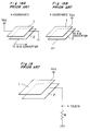
- Fig. 2 is a schematic perspective view of the touch panel input apparatus.
- a touch panel 11 of the apparatus is composed of two transparent electrode panels formed of analog resistance films. The two transparent electrode panels are overlaid on each other with a predetermined space interposed therebetween.
- the touch panel 11 is attached to a display device 14 such as a liquid crystal display panel or a CRT, as shown in Fig. 3. Input of characters and/or figures into the apparatus is carried out by pressing the touch panel 11 with a touch pen 12.
- a touch key 13 is provided on the touch panel 11 at a predetermined position thereof.
- the touch key 13 includes a printed sheet bonded to the touch panel 11.
- a display control circuit 15 controls a display storage 16 and the display device 14 50 that an image is displayed on the display device 14 according to image data stored in the display storage 16.
- a touch panel control circuit 17 applies voltages different from each other to both ends of each electrode panel constituting the touch panel 11 to form a voltage distribution (voltage inclination) in each electrode panel.
- the touch panel control circuit 17 detects a position voltage generated on each electrode panel and outputs a signal indicating the voltage to an A/D converter 18.
- a RAM (Random Access Memory) 19 is used as a work area in which various kinds of control data have been stored.
- a ROM (Read Only Memory) 20 stores programs for a CPU 21.
- the CPU 21 controls the display control circuit 15 so as to write image data to the display storage 16 and display an image on the display device 14.
- the CPU 21 controls the touch panel control circuit 17 so as to switch over a voltage to be applied to each electrode panel of the touch panel 11 and calculate the coordinate of an inputted position on the touch panel 11, based on a signal representing the position voltage outputted thereto from the A/D converter 18. Calculation of the coordinate of the inputted position is achieved by collating a detected position voltage with the voltage inclination data stored in the RAM 19.
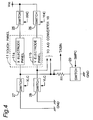
- Fig. 4 shows a part of the circuit of the touch panel control circuit 17, and the touch panel 11.
- the touch panel 11 consists of an upper, X-direction electrode panel 11a and a lower, Y-direction electrode panel 11b.
- Each of the X-direction and Y-direction electrode panels 11a and 11b has a resistor network having a uniform resistance distribution.
- One end of the X-direction electrode panel 11a is connected with a power source Vcc via a switch circuit 25 which is controlled to be turned on and off by a control signal XHC.
- the other end of the X-direction electrode panel 11a is grounded not only via a switch circuit 27 which is turned on and off by a control signal XLC, but also via an output resistor R1 and a switch 29 which is turned on and off by a control signal SMPC, the output resistor R1 and the switch 29 being connected in series.
- one end of the Y-direction electrode panel 11b is connected with the power source Vcc via a switch circuit 26 which is turned on and off by a control signal YHC, while the other end thereof is grounded via a switch circuit 28 which is turned on and off by a control signal YLC.
- the said other end of the X-direction electrode panel 11a and that of the Y-direction electrode panel 11b are also connected with the A/D converter 18 and the control circuit provided subsequently to the A/D converter 18.
- the touch panel input apparatus having the construction as described above is operated as will be described below under the control of the CPU 21 to detect the coordinate of the inputted position on the touch panel 11.
- the electrode panels 11a and 11b each have a uniform resistance distribution.
- the voltage of the power source Vcc is applied across the X-direction electrode panel 11a by setting the levels of the control signals XHC and XLC to "H" to turn on the switch circuits 25 and 27.
- the uniform voltage distribution is generated in the X-direction electrode panel 11a.
- the other switch circuits 26 and 28 are turned off by setting the levels of the control signals YHC and YLC to "L".
- the electrode panels 11a and 11b are electrically connected with each other at the pressed point, which causes a voltage corresponding to the pressed position on the X-direction electrode panel 11a to be developed in the Y-direction electrode panel 11b positioned below the X-direction electrode panel 11a of the touch panel 11.
- the A/D converter 18 performs an analog-to-digital conversion of the voltage as the position voltage, and outputs the digital value of the voltage to the CPU 21. Based on the position voltage, the CPU 21 calculates the X-coordinate of the pressed position, as described above.
- the voltage of the power source Vcc is applied across the Y-direction electrode panel 11b by setting the levels of the control signals YHC and YLC to "H" to turn on the switch circuits 26 and 28. As a result, a uniform voltage distribution is generated in the Y-direction electrode panel 11b. Further, the levels of the control signals XHC and XLC are set to "L" to turn off the switch circuits 25 and 27.
- the A/D converter When a point of the X-direction electrode panel 11a is pressed with the touch pen 12, the A/D converter performs the analog-to-digital conversion of a position voltage which has appeared on the X-direction electrode panel 11a, and outputs the digital value of the voltage to the CPU 21. Based on the position voltage, the CPU 21 calculates the Y-coordinate of the pressed position, as described above.
- the X-coordinate and Y-coordinate of the pressed position are alternately detected by time sharing by alternately turning on the switch circuits 25 and 27 and turning off the switch circuits 26 and 28, and turning off the switch circuits 25 and 27 and turning on the switch circuits 26 and 28, respectively.
- a power-on operation is performed by pressing the X-direction electrode panel 11a during a power-off state of the apparatus.
- the level of each of the control signals XHC, XLC, and YLC is set to "L", while the level of each of the control signals YHC and SMPC is set to "H”.
- the end of the Y-direction electrode panel 11b is connected with the power source Vcc, while the end of the X-direction electrode panel 11a is grounded via the output resistor R1.
- the X-direction and Y-direction electrode panels 11a and 11b are electrically connected with each other to form a series circuit of the Y-direction electrode panel 11b, the X-direction electrode panel 11a, and the output resistor R1 between the power source Vcc and the GND.
- electric current flows in the order of the power source Vcc ⁇ the switch circuit 26 ⁇ the Y-direction electrode panel 11b ⁇ the X-direction electrode panel 11a ⁇ the output resistor R1 ⁇ the switch circuit 29 ⁇ the GND.
- a value of a voltage which appears between both ends or terminals of the output resistor R1 is obtained by dividing the power source voltage Vcc by the resistance value of the output resistor R1 plus the resistance values of both the X-direction and Y-direction electrode panels 11a and 11b [(a resistance value between the power source Vcc and the contact point on the Y-direction electrode panel 11b) + (a contact resistance value between the X-direction and Y-direction electrode panels 11a and 11b) + (a resistance value between the contact point on the X-direction electrode panel 11a and a connection point at which the output resistor R1 is connected)].
- the power-on operation can be accomplished by the input signal TABIN through the intermittent sampling of the input signal TABIN.
- Fig. 5 is a circuit diagram of a sampling circuit which constitutes a part of the touch panel control circuit 17 and samples the input signal TABIN.
- Figs. 6A-6I are timing charts for the sampling circuit.
- the sampling circuit has an input buffer 30 having a function of preventing a through-electric current from flowing therethrough, flip-flops 31 and 36, an OR gate 32, invertors 33 and 34, a NAND gate 35, and a delay circuit 37.
- a clock signal CLK to be inputted to the OR gate 32 has a low frequency, for example, 32 Hz.
- the clock signal CLK is generated by a clock circuit.
- the flip-flop 36 is controlled by the CPU 21 such that the level of a signal A is set to "H” when the sampling circuit is operated and to "L” when the operation of the sampling circuit is stopped.
- the flip-flop 31 is reset and a signal ON for causing the CPU 21 to execute the power-on operation is also set at a "L" level. Thus, the CPU 21 does not execute the power-on operation.
- the level of the signal C is "H"
- the level of each of the control signals YHC and SMPC to be outputted from the delay circuit 37 to the switch circuits 26 and 29 becomes “L”.
- one end of the Y-direction electrode panel 11b and the output resistor R1 are not electrically connected with the power source Vcc and the GND, respectively. Accordingly, a voltage does not appear at both ends of the output resistor R1, and thus the level of the input signal TABIN becomes "L".
- the input buffer 30 goes into an input inhibit mode.
- the input signal TABIN has an intermediate potential between the voltage of the power source Vcc and the ground voltage, a through-electric current is prevented from flowing through a CMOS transistor constituting the input buffer 30.
- the level of an output signal of the delay circuit 37 becomes “L”; the input buffer 30 goes into an input-inhibit mode; and the level of each of the control signals YHC and SMPC also becomes “L”.
- the use of the delay circuit 37 delays the timing at which the flip-flop 31 enters the input-inhibit mode and the timing at which the level of each of the control signals YHC and SMPC becomes “L” until the latch operation of the flip-flop 31, which is started at the leading edge of the signal C, is completed.
- the CPU 21 controls the flip-flop 36 to set the level of the signal A to "L" in a time period (e) shown in Fig. 6A. As a result, the flip-flop 31 is reset and consequently, the level of the signal ON becomes "L".
- the CPU 21 when the CPU 21 has completed the power-on operation, the CPU 21 resets the flip-flop 31 which latches the input signal TABIN. Thereafter, the sampling of the input signal TABIN is not executed. Hence, electric current is not wasted. Further, the input signal TABIN is inputted to the flip-flop 31 via the input buffer 30 designed such that the through or pass electric current is prevented from flowing therethrough. Specifically, when the control signals YHC and SMPC are at a "L" level, the input buffer 30 goes into the input inhibit mode, so that, even when the input signal TABIN has an intermediate potential between the power voltage Vcc and the ground voltage, a through electric current does not flow through the input buffer 30.
- the flip-flop 31 holds the state of the signal D, which becomes an "H" level when the level of the input signal TABIN has exceeded a threshold ⁇ of the input buffer 30, until the CPU 21 releases it.
- the CPU 21 is reliably capable of recognizing a power-on instruction.
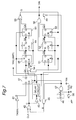
- Fig. 7 is a circuit diagram of a sampling circuit different from that shown in Fig. 3.
- Fig. 3 is a timing chart of the sampling circuit shown in Fig. 7.
- the sampling circuit has a card locking switch 58 serving as an outer factor switch. This sampling circuit is designed to start the power-on operation when pressing of the touch panel 11 has been detected three times in sequence.
- the sampling circuit has an input buffer 40, flip-flops 41 and 46, invertors 43 and 44, a NAND gate 45, and a delay circuit 47.
- Each of these members has the same construction and operation as those of each of the input buffer 30, the flip-flops 31 and 36, the OR gate 32, the invertors 33 and 34, the NAND gate 35, and the delay circuit 37 of the sampling circuit shown in Fig. 5.
- the sampling circuit has flip-flops 48 - 53, an OR gate 54, a 3-input NOR gate 55, a 3-input AND gate 56, and an AND gate 57.
- the sampling circuit having the above construction performs a sampling operation as will be described below with reference to the timing charts shown in Figs. 8A-8R.
- the flip-flop 41 is reset, and the level of an output signal Q1 thereof becomes “L” as in the sampling circuit shown in Fig. 5. Because the level of the signal ON is also “L”, the level of the signal C is always “H”, and thus the sampling operation is stopped. The level of each of the control signals YHC and SMPC also becomes “L”, and thus the input buffer 40 goes into the input inhibit mode.
- the level of the signal Q1 outputted from the flip-flop 41 becomes “H” when the touch panel is kept to be pressed as in a time period (g), and hence, the level of the output signal Q2 of the flip-flop 48 also becomes “H”.
- the level of the output signal G of the 3-input NOR gate 55 becomes “L”
- the level of the signal ON also becomes “L”, so that the power-on operation is not performed.
- the level of the output signal G of the 3-input NOR gate 55 becomes “H”
- the level of a signal F outputted from the OR gate 54 to the flip-flops 48 - 50 as a clock signal therefor is fixed at "H”
- the latch operation of the flip-flops 48 - 50 is stopped.
- the flip-flops 51 - 53 are released from the reset state and the latch operation thereof is started. Because the touch panel is not pressed as described above, the level of the signal ON is "L".
- the touch panel When the touch panel is pressed at a point thereof with the touch pen and as a result, the X-electrode and Y-electrode panels are brought into contact with each other during the sampling operation in the time period (h), the voltage of the input signal TABIN rises synchronously with the level "H" of the control signals YHC and SMPC in a time period (i) shown in Fig. 8R.
- the level of the input signal TABIN has exceeded the threshold ⁇ of the input buffer 40, the level of the signal D inputted to the flip-flop 41 becomes "H", and the input signal TABIN is latched at the rise of the signal C (i.e., the clock signal CLK).
- the flip-flops 51 - 53 sequentially latch the input signal TABIN at the step-down or trailing edge of the clock signal CLK, and as a result, the levels of the output signals Q5 - Q7 become "H” sequentially.
- the level of each of the output signals Q5 - Q7 has become “H”
- the level of the signal ON outputted from the 3-input AND gate 56 to the CPU 21 becomes “H”
- the CPU 21 starts the power-on operation.
- the card locking switch 58 is closed when an IC card is releasably inserted in the apparatus, whereas the card locking switch 58 is open when the inserted IC card is locked so that it is not releasable.
- the card locking switch 58 When the inserted IC card gets removable in the time period (i) shown in Fig. 8R, the card locking switch 58 is turned on. Then, the voltage level at a contact point H becomes "L” in a time period (j), and the level of the output signal of the AND gate 57 also becomes “L”. As a result, the flip-flop 41 is reset, the flip-flops 48 - 50 are preset, and the flip-flops 51 - 53 are reset.
- the level of the signal ON to be supplied to the CPU 21 becomes "L” and hence, the CPU 21 does not perform the power-on operation.
- the card locking switch 58 is turned. As a result, the flip-flop 41 is reset, the flip-flops 48 - 50 are preset, and the flip-flops 51 - 53 are reset.
- the card locking switch 58 When the IC card is brought into a locked state in the time period (j), the card locking switch 58 is turned off or open. Then, the level of the output signal of the AND gate 57 becomes "H". This state is the same as the state in which the level of the signal A has become “H” under the control of the CPU 21 in the time period (g). Therefore, the time period (g) starts and it is checked whether or not a tablet keeps being pressed.
- the sampling circuit shown in Fig. 7 has the flip-flops 48 - 50 and 51 - 53 for detecting that the touch panel 11 has been pressed in a power-off state by sequentially latching the output signal Q1 of the flip-flop 41 having a function of latching the input signal TABIN.
- the flip-flops 51 - 53 are reset so that the sampling operation is stopped, if any one of the output signals Q2 - Q4 of each of the flip-flops 48 - 50 has become "H", i.e., when the touch panel 11 has been pressed.
- a "stop key” which is one of the touch keys 13 mounted on the touch panel 11 is pressed to turn off power.
- the CPU 21 decides that a pressed position of the touch panel 11 is in the stop key region, thus executing the power-off operation.
- the sampling operation is started by setting the signal A outputted from the flip-flop 46 of the sampling circuit to an "H" level. If the stop key region of the touch panel 11 is kept pressed at this time, an instruction of turning on the power source is not issued to the CPU 21.
- the CPU 21 executes the power-on operation when the levels of the output signals Q5 - Q7 of the flip-flops 51 - 53 have all become "H".
- the power-on operation is not started unless the pressed state of the touch panel 11 continues for a time corresponding to at least three sampling periods. In this manner, the execution of the power-on operation due to penetration of noise such as an instantaneous static electricity is prevented.
- the sampling circuit of Fig. 7 is provided with the card locking switch 58 designed to be open while the IC card is locked.
- the card locking switch 58 When the IC card is unlocked and thus the card locking switch 58 is turned on, the flip-flop 41 is reset and the input buffer 40 is placed in the input-inhibition mode. Accordingly, in the sampling circuit, if the IC card is in a removable state, the sampling operation is stopped to prevent an instruction indicating the execution of the power-on operation from being issued to the CPU 21.
- this construction prevents malfunction from occurring due to insertion and/or removal of the IC card while the CPU 21 is in operation.
- the program goes to a subsequent step after detecting three times nonpressing of the touch panel after the level of the signal A becomes "H" in the power-off state.
- the number of detection times can be increased or decreased according to the number of the flip-flops 48 - 50.
- instructions to turn on power i.e., to perform the power-on operation
- the number of detection times for the issuance of the instructions can be also increased or decreased according to the number of the flip-flops 51-53.
- a sampling circuit shown in Fig. 9 stops a sampling operation if the nonpressed state of the touch panel is detected once when the level of the signal A becomes "H" in the power-off state.
- the sampling circuit give an instruction to execute the power-on operation if a pressed state of the touch panel is detected once in the state in which the power source can be turned on.
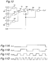
- Fig. 10 is a circuit diagram of a clock signal generation circuit for generating the clock signal CLK to be inputted to the OR gates 32 and 42 of the sampling circuit shown in Figs. 5 and 7, respectively.
- clock signals CLK1, CLK2, and CLK3 having frequencies three times, six times, and 12 times as high as that of the clock signal CLK, respectively are inputted to each of AND gates 61 - 63.
- Output signals of flip-flops 64 - 66 are inputted to the AND gates 61 - 63, respectively.
- the level of the output signal of each of the flip-flops 64 - 66 is set by the CPU 21.
- Output signals of the AND gates 61 - 63 are inputted to a 3-input OR gate 67.
- the frequency of the clock signal to be supplied to a flip-flop 68 can be selected depending on the level of the output signal of each of the flip-flops 64 - 66.
- the clock signal CLK1 is inputted to the 3-input OR gate 67.
- the clock signal CLK1 is inputted to the flip-flop 68 as the clock thereof.
- Figs. 12A-12E and 13A-13E are timing charts of the clock signal-generation circuit shown in Fig. 10.
- Fig. 12A through 12E are timing charts showing the case in which the clock signal CLK1 is inputted to the flip-flop 68 as the clock thereof.
- Fig. 13A through 13E are timing charts showing the case in which the clock signal CLK2 is inputted to the flip-flop 68 as the clock thereof.
- the output signal Q8 of the flip-flop 68 is inputted to a NAND gate 70 via an invertor 69.
- the level of an output signal CLK' of the NAND gate 70 becomes “L” only when the level of the clock signal CLK is "H” and that of the output signal Q8 is “L". That is, each time period (k, l) in which the level of the output signal CLK' is "L” appears in the half cycle of any one of the clock signals CLK1 - CLK3 selected by the flip-flops 64 - 66.
- the output signal CLK' is a clock signal generated by changing the time period in which the level of the output signal CLK is "L” by means of any one of the clock signals CLK1 - CLK3.
- the clock signal CLK' generated in this manner is inputted to each of the sampling circuits as the clock signal CLK.
- the time period in which the voltage of the power source Vcc is applied to the touch panel 11 can be changed by altering the time width of the "L" level of the clock signal CLK, namely, the clock signal CLK' to be inputted to the sampling circuits.
- the clock generation circuit if there is a difference in time required from the application of the power voltage Vcc to the touch panel 11 until the turning to an "H" level of the input signal TABIN, depending on the characteristic of the touch panel 11 and the size of a capacitor provided on an input signal line, the "L" level period of the clock signal CLK is controlled so that the time period in which the power voltage Vcc is applied to the touch panel 11 is adjusted so as to allow the level of the input signal TABIN to become reliably "H".
- the frequency of the clock signal CLK is multiplied by an integer to obtain the clock signals CLK1, CLK2, and CLK3, but they can be obtained by dividing a reference clock signal having a higher frequency.
- the execution of the power-on operation can be prevented from being erroneously started by setting or specifying a position in the touch panel 11 in which the touch panel is to be pressed in issuing the power-on operation to the CPU 21, even though an operator's hand or other persons' hands touch the touch panel 11 by accident.
- Fig. 14 is an explanatory view showing a touch panel 71 having a region in which the power-on operation is started when the region is pressed and a region in which the power-on operation is not started when it is pressed.
- the touch panel 71 is provided with a region A which is surrounded by coordinates (X A1 , Y A1 ), (X A1 , Y A2 ), (X A2 , Y A2 ), and (X A2 , Y A1 ) and pressing of which causes the power-on operation to be started, and a region B which does not cause the power-on operation to be started when pressed.
- the coordinates (X A1 , Y A1 ) and (X A2 , Y A2 ) are stored in the RAM 19.
- Fig. 15 is a flowchart of the power-on control operation to be executed by the CPU 21 and the touch panel control circuit 17 when the touch panel 71 is used.
- the sampling circuit to be mounted on the touch panel control circuit 17 is the sampling circuit (wherein detection number of nonpressing/pressing of the touch panel 71 is "N") shown in Fig. 7.
- step S1 It is decided at step S1 whether nonpressing of the touch panel 71 has been detected N times in the sampling circuit. If YES, the program goes to step S2.
- step S2 It is decided at step S2 whether pressing of the touch panel 71 has been detected N times in the sampling circuit. If YES, the program goes to step S3.
- the CPU 21 controls the touch panel control circuit 17 such that a voltage inclination occurs alternately in the X-direction and Y-direction electrode panels 11a and 11b whereby a position voltage is detected, as described previously. Then, the CPU 21 detects the coordinate of an input position (i.e., a pressed position) on the touch panel 71, based on the position voltage and the data of the voltage inclination, as described previously.
- an input position i.e., a pressed position
- the CPU decides at step S4 whether or not the pressed position on the touch panel 71 is in the region A, based on the detected coordinates of the pressed position on the touch panel 71 and the coordinates (X A1 , Y A1 ) and (X A2 , Y A2 ) stored in the RAM 19. If YES, the program goes to step S5. If NO, the program returns to step S1.
- step S5 the CPU 21 executes the power-on operation. In this way, the power-on control operation is completed.
- the processings at steps S3 through S5 are executed by the CPU 21 activated by the signal ON having an "H" level, which is outputted thereto from the sampling circuit at step S2.
- This mode allows the apparatus to have a secret function of preventing persons other than the owner thereof from using it.
- the secret function can be obtained by designing the apparatus such that the power-on operation is started by a specific input operation such as "drawing a circle” as shown in Fig. 16A, “drawing a triangle” as shown in Fig. 16B, “touch the touch panel three times” as shown in Fig. 16C, “write the user's name” as shown in Fig. 16D, etc.
- Fig. 17 is a flowchart of the power-on control operation to be executed by the CPU 21 and the touch panel control circuit 17 when the power-on operation is executed by performing a specific operation as described above.
- the sampling circuit to be mounted on the touch panel control circuit 17 is the sampling circuit shown in Fig. 5.
- the RAM 19 previously stores a result produced by the specific input operation. That is, "figure ⁇ ", “figure ⁇ ”, “number of touches", and "specific character or characters” are stored in advance in the RAM 19 in correspondence with the input operations shown in Figs. 16A, 16B, 16C, and 16D, respectively.
- step S11 It is decided at step S11 whether or not the touch panel 11 has been pressed. If YES, the program goes to step S12.
- the CPU 21 controls a pen-input recognizing portion (not shown) so as to recognize an input result of the input operation executed at step S11.
- step S13 It is decided at step S13 whether or not the input operation result recognized at step S12 by the CPU 21 coincides with the input result stored in the RAM 19. If YES, the program goes to step S14, whereas if NO, the program returns to step S11.
- step S14 the CPU 21 executes a power-on operation. In this way, the power-on control operation is completed.
- the processings at steps S12 through S14 are executed by the CPU 21 activated by the signal ON having an "H" level outputted thereto from the sampling circuit at step S11.
- the algorithm of the power-on control operation is not limited to that of the flowcharts shown in Figs. 15 and 17.
Landscapes
- Engineering & Computer Science (AREA)
- General Engineering & Computer Science (AREA)
- Theoretical Computer Science (AREA)
- Human Computer Interaction (AREA)
- Physics & Mathematics (AREA)
- General Physics & Mathematics (AREA)
- Position Input By Displaying (AREA)
Applications Claiming Priority (3)
| Application Number | Priority Date | Filing Date | Title |
|---|---|---|---|
| JP266622/94 | 1994-10-31 | ||
| JP26662294A JP3269596B2 (ja) | 1994-10-31 | 1994-10-31 | タッチパネル式入力装置 |
| JP26662294 | 1994-10-31 |
Publications (3)
| Publication Number | Publication Date |
|---|---|
| EP0709762A2 true EP0709762A2 (fr) | 1996-05-01 |
| EP0709762A3 EP0709762A3 (fr) | 1996-10-30 |
| EP0709762B1 EP0709762B1 (fr) | 2001-09-12 |
Family
ID=17433379
Family Applications (1)
| Application Number | Title | Priority Date | Filing Date |
|---|---|---|---|
| EP95109263A Expired - Lifetime EP0709762B1 (fr) | 1994-10-31 | 1995-06-14 | Dispositif d'entrée à panneau de contact avec une opération d'échantillonnage intermittente |
Country Status (4)
| Country | Link |
|---|---|
| US (1) | US5777604A (fr) |
| EP (1) | EP0709762B1 (fr) |
| JP (1) | JP3269596B2 (fr) |
| DE (1) | DE69522637T2 (fr) |
Cited By (3)
| Publication number | Priority date | Publication date | Assignee | Title |
|---|---|---|---|---|
| GB2443056A (en) * | 2004-03-19 | 2008-04-23 | Igt Reno Nev | Touch screen apparatus |
| US7663606B2 (en) | 2004-03-19 | 2010-02-16 | Igt | Apparatus and method for configuring a touch screen |
| US7855717B2 (en) | 2004-03-19 | 2010-12-21 | Igt | Touch screen apparatus and method |
Families Citing this family (26)
| Publication number | Priority date | Publication date | Assignee | Title |
|---|---|---|---|---|
| US5977957A (en) * | 1997-05-22 | 1999-11-02 | Ericsson Inc. | Adaptive sampling of touch screen input |
| US6058485A (en) * | 1997-07-29 | 2000-05-02 | Lsi Logic Corporation | Method and apparatus for managing power consumption of a digitizing panel |
| US6215477B1 (en) * | 1997-10-22 | 2001-04-10 | Smart Technologies Inc. | Touch sensitive display panel |
| JP3595137B2 (ja) * | 1997-11-14 | 2004-12-02 | シャープ株式会社 | 液晶タブレット装置 |
| US6236787B1 (en) | 1998-07-08 | 2001-05-22 | Optical Switch Corporation | Method and apparatus for aligning optical fibers using an alignment spacer |
| US6204897B1 (en) * | 1998-08-18 | 2001-03-20 | International Business Machines Corporation | Integrated resistor for measuring touch position in a liquid crystal display device |
| JP4939682B2 (ja) * | 1999-04-27 | 2012-05-30 | エーユー オプトロニクス コーポレイション | 表示装置 |
| JP4094794B2 (ja) * | 1999-09-10 | 2008-06-04 | 株式会社リコー | 座標検出装置、情報記憶媒体および座標検出方法 |
| US6862018B2 (en) * | 2001-11-01 | 2005-03-01 | Aiptek International Inc. | Cordless pressure-sensitivity and electromagnetic-induction system with specific frequency producer and two-way transmission gate control circuit |
| JP4000001B2 (ja) * | 2002-04-22 | 2007-10-31 | 松下電器産業株式会社 | クロック制御装置およびクロック制御方法 |
| WO2004040538A1 (fr) * | 2002-10-28 | 2004-05-13 | Semtech Corporation | Acquisition de donnees a partir d'un clavier tactile capacitif |
| TW200805128A (en) * | 2006-05-05 | 2008-01-16 | Harald Philipp | Touch screen element |
| US20080136808A1 (en) * | 2006-12-12 | 2008-06-12 | General Instrument Corporation | Method and System for Illuminating a Display Screen of a Handheld Electronic Device |
| US7812830B2 (en) * | 2007-03-12 | 2010-10-12 | Texas Instruments Incorporated | Touch-initiated power-saving clock system and method for touch screen controller |
| US20090096762A1 (en) * | 2007-10-16 | 2009-04-16 | Epson Imaging Devices Corporation | Input device, display device with input function, and electronic apparatus |
| KR101427586B1 (ko) * | 2007-12-26 | 2014-08-07 | 삼성디스플레이 주식회사 | 표시 장치 및 그 구동 방법 |
| KR20090089254A (ko) | 2008-02-18 | 2009-08-21 | 세이코 엡슨 가부시키가이샤 | 센싱 장치, 표시 장치, 전자 기기 및, 센싱 방법 |
| JP4775386B2 (ja) * | 2008-02-18 | 2011-09-21 | ソニー株式会社 | センシング装置、表示装置、電子機器およびセンシング方法 |
| KR100957836B1 (ko) * | 2008-06-02 | 2010-05-14 | 주식회사 애트랩 | 터치패널 장치 및 이의 접촉위치 검출방법 |
| JP5106268B2 (ja) * | 2008-06-24 | 2012-12-26 | 富士通コンポーネント株式会社 | タッチパネル |
| EP2352073A4 (fr) | 2008-11-05 | 2013-10-02 | Nec Corp | Dispositif électronique portable, procédé d'économie d'énergie dans un dispositif électronique portable, et programme d'économie d'énergie |
| JP5642500B2 (ja) * | 2010-07-22 | 2014-12-17 | 富士通コンポーネント株式会社 | タッチパネルにおける位置検出方法、タッチパネル、タッチパネルの初期化方法 |
| JP6342141B2 (ja) * | 2013-11-15 | 2018-06-13 | 富士通コンポーネント株式会社 | タッチパネル装置及びタッチパネル装置の制御方法 |
| KR20160012350A (ko) * | 2014-07-23 | 2016-02-03 | 삼성디스플레이 주식회사 | 가변 게이트 클록 발생기, 이를 포함하는 디스플레이 장치 및 디스플레이 장치의 구동 방법 |
| JP7423428B2 (ja) * | 2020-06-05 | 2024-01-29 | シャープ株式会社 | タッチパネル入力装置 |
| JP7582922B2 (ja) * | 2021-09-03 | 2024-11-13 | 株式会社東海理化電機製作所 | 検出装置 |
Citations (1)
| Publication number | Priority date | Publication date | Assignee | Title |
|---|---|---|---|---|
| JPH05127827A (ja) | 1991-11-01 | 1993-05-25 | Sharp Corp | タツチパネル式入力装置 |
Family Cites Families (7)
| Publication number | Priority date | Publication date | Assignee | Title |
|---|---|---|---|---|
| JP3193039B2 (ja) * | 1990-11-20 | 2001-07-30 | キヤノン株式会社 | 電子装置及び情報処理方法 |
| CA2059498A1 (fr) * | 1991-01-22 | 1992-07-23 | Hideki Takahara | Appareil de saisie et d'affichage de donnees |
| JP2656167B2 (ja) * | 1991-05-30 | 1997-09-24 | シャープ株式会社 | タブレット入力装置 |
| JPH05108218A (ja) * | 1991-10-11 | 1993-04-30 | Toshiba Corp | コンピユータシステム |
| JPH06119090A (ja) * | 1992-10-07 | 1994-04-28 | Hitachi Ltd | 省電力制御方式 |
| JP2955149B2 (ja) * | 1993-05-11 | 1999-10-04 | グンゼ株式会社 | タッチパネルの座標検出装置 |
| US5568409A (en) * | 1994-12-14 | 1996-10-22 | Tritech Microelectronics International Pte Ltd. | Tablet with system power saving features including reactivation by pen contact after inactive period |
-
1994
- 1994-10-31 JP JP26662294A patent/JP3269596B2/ja not_active Expired - Lifetime
-
1995
- 1995-06-06 US US08/467,294 patent/US5777604A/en not_active Expired - Lifetime
- 1995-06-14 EP EP95109263A patent/EP0709762B1/fr not_active Expired - Lifetime
- 1995-06-14 DE DE69522637T patent/DE69522637T2/de not_active Expired - Lifetime
Patent Citations (1)
| Publication number | Priority date | Publication date | Assignee | Title |
|---|---|---|---|---|
| JPH05127827A (ja) | 1991-11-01 | 1993-05-25 | Sharp Corp | タツチパネル式入力装置 |
Cited By (4)
| Publication number | Priority date | Publication date | Assignee | Title |
|---|---|---|---|---|
| GB2443056A (en) * | 2004-03-19 | 2008-04-23 | Igt Reno Nev | Touch screen apparatus |
| GB2443056B (en) * | 2004-03-19 | 2008-06-11 | Igt Reno Nev | A touch screen apparatus |
| US7663606B2 (en) | 2004-03-19 | 2010-02-16 | Igt | Apparatus and method for configuring a touch screen |
| US7855717B2 (en) | 2004-03-19 | 2010-12-21 | Igt | Touch screen apparatus and method |
Also Published As
| Publication number | Publication date |
|---|---|
| DE69522637D1 (de) | 2001-10-18 |
| EP0709762B1 (fr) | 2001-09-12 |
| EP0709762A3 (fr) | 1996-10-30 |
| US5777604A (en) | 1998-07-07 |
| DE69522637T2 (de) | 2002-07-04 |
| JPH08129444A (ja) | 1996-05-21 |
| JP3269596B2 (ja) | 2002-03-25 |
Similar Documents
| Publication | Publication Date | Title |
|---|---|---|
| EP0709762B1 (fr) | Dispositif d'entrée à panneau de contact avec une opération d'échantillonnage intermittente | |
| EP0457990B1 (fr) | Appareil de traitement de données interactif utilisant un crayon | |
| JP2822526B2 (ja) | 個人用情報処理装置及び個人用情報処理方法 | |
| CA1312962C (fr) | Dispositif de commande d'affichage de messages de guidage | |
| US6239792B1 (en) | Coordinate input system having multiple editing modes | |
| JP3235480B2 (ja) | タッチパネル入力装置 | |
| US20020057263A1 (en) | Simulating gestures of a pointing device using a stylus and providing feedback thereto | |
| EP0271280A2 (fr) | Arrangement pour utiliser dans un ordinateur | |
| US6411300B1 (en) | Processing apparatus | |
| EP0513635B1 (fr) | Appareil de traitement de données pour la commande de positions de fenêtre | |
| US20010040554A1 (en) | Virtual keyboard | |
| JP2000146629A (ja) | 測定装置用ヘルプ画面情報表示装置 | |
| US5461222A (en) | Memory card | |
| JP2822569B2 (ja) | 情報処理装置及び情報処理方法 | |
| WO1994016408A1 (fr) | Procede et appareil de correction d'ecriture a l'encre electronique | |
| JPH05150926A (ja) | 情報処理装置 | |
| JP2866575B2 (ja) | 感圧式タブレットおよび情報処理装置 | |
| JPH07219700A (ja) | 情報処理装置 | |
| JP3238065B2 (ja) | 情報処理装置及び情報処理装置での基準筆圧設定方法 | |
| JPH07200152A (ja) | タブレット入力電子機器 | |
| JP4521888B2 (ja) | 出力信号制御装置及び方法及び座標入力装置及び記憶媒体 | |
| JPH03111926A (ja) | データ処理装置 | |
| JP3256023B2 (ja) | 情報処理装置 | |
| JP3318759B2 (ja) | 情報処理装置および情報処理方法 | |
| EP1411420A1 (fr) | Méthode de détermination de coordonnées du point de contact pour utilisation dans un écran tactil résistif |
Legal Events
| Date | Code | Title | Description |
|---|---|---|---|
| PUAI | Public reference made under article 153(3) epc to a published international application that has entered the european phase |
Free format text: ORIGINAL CODE: 0009012 |
|
| AK | Designated contracting states |
Kind code of ref document: A2 Designated state(s): DE FR GB |
|
| PUAL | Search report despatched |
Free format text: ORIGINAL CODE: 0009013 |
|
| AK | Designated contracting states |
Kind code of ref document: A3 Designated state(s): DE FR GB |
|
| 17P | Request for examination filed |
Effective date: 19970128 |
|
| GRAG | Despatch of communication of intention to grant |
Free format text: ORIGINAL CODE: EPIDOS AGRA |
|
| 17Q | First examination report despatched |
Effective date: 20001221 |
|
| GRAG | Despatch of communication of intention to grant |
Free format text: ORIGINAL CODE: EPIDOS AGRA |
|
| GRAH | Despatch of communication of intention to grant a patent |
Free format text: ORIGINAL CODE: EPIDOS IGRA |
|
| GRAG | Despatch of communication of intention to grant |
Free format text: ORIGINAL CODE: EPIDOS AGRA |
|
| GRAH | Despatch of communication of intention to grant a patent |
Free format text: ORIGINAL CODE: EPIDOS IGRA |
|
| GRAH | Despatch of communication of intention to grant a patent |
Free format text: ORIGINAL CODE: EPIDOS IGRA |
|
| GRAA | (expected) grant |
Free format text: ORIGINAL CODE: 0009210 |
|
| AK | Designated contracting states |
Kind code of ref document: B1 Designated state(s): DE FR GB |
|
| REF | Corresponds to: |
Ref document number: 69522637 Country of ref document: DE Date of ref document: 20011018 |
|
| ET | Fr: translation filed | ||
| REG | Reference to a national code |
Ref country code: GB Ref legal event code: IF02 |
|
| PLBE | No opposition filed within time limit |
Free format text: ORIGINAL CODE: 0009261 |
|
| STAA | Information on the status of an ep patent application or granted ep patent |
Free format text: STATUS: NO OPPOSITION FILED WITHIN TIME LIMIT |
|
| 26N | No opposition filed | ||
| PGFP | Annual fee paid to national office [announced via postgrant information from national office to epo] |
Ref country code: GB Payment date: 20140611 Year of fee payment: 20 |
|
| PGFP | Annual fee paid to national office [announced via postgrant information from national office to epo] |
Ref country code: DE Payment date: 20140611 Year of fee payment: 20 |
|
| PGFP | Annual fee paid to national office [announced via postgrant information from national office to epo] |
Ref country code: FR Payment date: 20140609 Year of fee payment: 20 |
|
| REG | Reference to a national code |
Ref country code: DE Ref legal event code: R071 Ref document number: 69522637 Country of ref document: DE |
|
| REG | Reference to a national code |
Ref country code: GB Ref legal event code: PE20 Expiry date: 20150613 |
|
| PG25 | Lapsed in a contracting state [announced via postgrant information from national office to epo] |
Ref country code: GB Free format text: LAPSE BECAUSE OF EXPIRATION OF PROTECTION Effective date: 20150613 |