EP0709820A2 - Méthode de commande avec effet mémoire d'un panneau d'affichage à plasma en utilisant des tensions d'écriture et d'entretien indépendantes - Google Patents
Méthode de commande avec effet mémoire d'un panneau d'affichage à plasma en utilisant des tensions d'écriture et d'entretien indépendantes Download PDFInfo
- Publication number
- EP0709820A2 EP0709820A2 EP95116050A EP95116050A EP0709820A2 EP 0709820 A2 EP0709820 A2 EP 0709820A2 EP 95116050 A EP95116050 A EP 95116050A EP 95116050 A EP95116050 A EP 95116050A EP 0709820 A2 EP0709820 A2 EP 0709820A2
- Authority
- EP
- European Patent Office
- Prior art keywords
- display
- scan
- discharge
- pulse
- electrodes
- Prior art date
- Legal status (The legal status is an assumption and is not a legal conclusion. Google has not performed a legal analysis and makes no representation as to the accuracy of the status listed.)
- Withdrawn
Links
- 238000000034 method Methods 0.000 title claims description 7
- 230000001419 dependent effect Effects 0.000 claims abstract description 9
- 230000004044 response Effects 0.000 claims abstract description 8
- 230000000977 initiatory effect Effects 0.000 claims description 2
- 230000002459 sustained effect Effects 0.000 abstract description 2
- 238000005513 bias potential Methods 0.000 description 14
- 239000007789 gas Substances 0.000 description 9
- 150000002500 ions Chemical class 0.000 description 6
- 230000002093 peripheral effect Effects 0.000 description 6
- OAICVXFJPJFONN-UHFFFAOYSA-N Phosphorus Chemical compound [P] OAICVXFJPJFONN-UHFFFAOYSA-N 0.000 description 4
- 230000003247 decreasing effect Effects 0.000 description 4
- 238000010586 diagram Methods 0.000 description 4
- 238000007599 discharging Methods 0.000 description 4
- 229910052734 helium Inorganic materials 0.000 description 4
- 239000001307 helium Substances 0.000 description 4
- SWQJXJOGLNCZEY-UHFFFAOYSA-N helium atom Chemical compound [He] SWQJXJOGLNCZEY-UHFFFAOYSA-N 0.000 description 4
- 230000015572 biosynthetic process Effects 0.000 description 3
- 238000010276 construction Methods 0.000 description 3
- 229910052724 xenon Inorganic materials 0.000 description 3
- FHNFHKCVQCLJFQ-UHFFFAOYSA-N xenon atom Chemical compound [Xe] FHNFHKCVQCLJFQ-UHFFFAOYSA-N 0.000 description 3
- 230000001965 increasing effect Effects 0.000 description 2
- 230000001939 inductive effect Effects 0.000 description 2
- 230000037452 priming Effects 0.000 description 2
- 230000004888 barrier function Effects 0.000 description 1
- 230000008859 change Effects 0.000 description 1
- 238000004891 communication Methods 0.000 description 1
- 229910052743 krypton Inorganic materials 0.000 description 1
- DNNSSWSSYDEUBZ-UHFFFAOYSA-N krypton atom Chemical compound [Kr] DNNSSWSSYDEUBZ-UHFFFAOYSA-N 0.000 description 1
- 230000006386 memory function Effects 0.000 description 1
- 238000012986 modification Methods 0.000 description 1
- 230000004048 modification Effects 0.000 description 1
- 229910052754 neon Inorganic materials 0.000 description 1
- GKAOGPIIYCISHV-UHFFFAOYSA-N neon atom Chemical compound [Ne] GKAOGPIIYCISHV-UHFFFAOYSA-N 0.000 description 1
- 230000001360 synchronised effect Effects 0.000 description 1
- 230000000007 visual effect Effects 0.000 description 1
Images




Classifications
-
- G—PHYSICS
- G09—EDUCATION; CRYPTOGRAPHY; DISPLAY; ADVERTISING; SEALS
- G09G—ARRANGEMENTS OR CIRCUITS FOR CONTROL OF INDICATING DEVICES USING STATIC MEANS TO PRESENT VARIABLE INFORMATION
- G09G3/00—Control arrangements or circuits, of interest only in connection with visual indicators other than cathode-ray tubes
- G09G3/20—Control arrangements or circuits, of interest only in connection with visual indicators other than cathode-ray tubes for presentation of an assembly of a number of characters, e.g. a page, by composing the assembly by combination of individual elements arranged in a matrix no fixed position being assigned to or needed to be assigned to the individual characters or partial characters
- G09G3/22—Control arrangements or circuits, of interest only in connection with visual indicators other than cathode-ray tubes for presentation of an assembly of a number of characters, e.g. a page, by composing the assembly by combination of individual elements arranged in a matrix no fixed position being assigned to or needed to be assigned to the individual characters or partial characters using controlled light sources
- G09G3/28—Control arrangements or circuits, of interest only in connection with visual indicators other than cathode-ray tubes for presentation of an assembly of a number of characters, e.g. a page, by composing the assembly by combination of individual elements arranged in a matrix no fixed position being assigned to or needed to be assigned to the individual characters or partial characters using controlled light sources using luminous gas-discharge panels, e.g. plasma panels
- G09G3/282—Control arrangements or circuits, of interest only in connection with visual indicators other than cathode-ray tubes for presentation of an assembly of a number of characters, e.g. a page, by composing the assembly by combination of individual elements arranged in a matrix no fixed position being assigned to or needed to be assigned to the individual characters or partial characters using controlled light sources using luminous gas-discharge panels, e.g. plasma panels using DC panels
Definitions
- the present invention relates to a memory drive for use in a direct-current plasma display panel (DC-PDP) which is expected to implement a thin and extended display screen suitable for displaying high-definition television (Hi-Vision) pictures, for example.
- DC-PDP direct-current plasma display panel
- Hi-Vision high-definition television
- FIG. 1 is a schematic circuit diagram of the conventional DC-PDP and its peripheral circuit.
- the DC-PDP 10 comprises a plurality of display discharge anodes or display electrodes 11-1 N , where N is a positive integer, auxiliary anodes or electrodes 21-2 J and cathodes or scan electrodes 31-3 M , where M is a positive integer.
- display cells 4 mn 1 ⁇ n ⁇ N , 1 ⁇ m ⁇ M
- auxiliary cells 5 mj 1 ⁇ j ⁇ L ).
- Coupled to the display discharge anodes I1-I N are anode drive circuits 111-11 N , respectively. Also coupled to the auxiliary anodes 21-2 J are a single auxiliary anode drive circuit 12. Further, coupled to the cathodes 31-3 M are cathode drive circuits 131-13 M , respectively.
- FIG. 2 shows the waveforms and is useful for understanding the memory drive for use in the conventional DC-PDP described in the above-referenced Yoshimichi Takano article.
- write pulses Pw as information to be displayed are applied from the anode drive circuits 111-11 N to the display discharge anodes I1-I N , respectively.
- the write pulse Pw takes its high level only when a writing is conducted to a desired display cell 4 mn .
- scan pulses Pscn and the subsequent sustain pulses Psus are sequentially applied from the cathode drive circuits 131-13 M to the cathodes 31-3 M , respectively.
- Auxiliary discharge pulses Psa are applied from an auxiliary anode drive circuit 12 to the auxiliary anodes 21-2 J at the same timing.
- the display discharge anodes I1-I N form a display electrode group, while the cathodes 31-3 M do a scan electrode group.
- FIG. 3 plots the relation between the current and voltage in the display cell shown in FIG. 1, with its abscissas denoting a discharge current I and ordinates denoting a voltage V between the anode and the cathode.
- Increment of the voltage V between the display discharge anodes I n and the cathode 3 m in the display cell 4 mn involves increment of the discharge current I at approximately the same rate to increment of the voltage, as plotted in FIG. 3.
- Such a characteristic of current I and voltage V is referred to as an I-V characteristic.
- V ⁇ denotes the V-segment of the I-V characteristic, which is the value intersecting the vertical axis of the graph and below which no discharge occurs in the cells.
- the voltage V ⁇ is about 220 volts in the I-V characteristic of the display cell 4 mn , while the voltage V ⁇ is about 230 volts in the auxiliary discharge cell 5 mj .
- the voltage between the high level of potential Vw of a write pulse Pw and the low level of potential Vscn of a scan pulse Pscn is given by 305 volts which causes the display cell 4 mn to initiate a write discharge.
- the voltage 255 volts between the low level of potential Vsus of a sustain pulse Psus, which is applied during a certain period of time subsequent to the write pulse Pw, and the low levelof potential V WL of the write pulse Pw serves to intermittently continue the sustain discharge so as to provide a memory function.
- the voltage between the high level of potential Vsa of an auxiliary discharge pulse Psa and the low level of potential Vscn of a scan pulse Pscn is given by 300 volts to conduct the auxiliary discharge which causes the display cell 4 mn to smoothly initiate the display discharge. If the potential Vscn and the potential Vsus are given by the same value, the circuit will be simplified in structure.
- FIG. 4 shows the waveforms and is useful for understanding another memory drive scheme of the conventional DC-PDP described in above-referenced Japanese patent laid-open publication No. 119740/1993.
- the voltage between the high level of potential of a write pulse Pw and the low level of potential of a scan pulse Pscn causes the display cell 4 mn to initiate the write discharge.
- the voltage between the low level of potential of a sustain pulse Psus, which is applied during a certain period of time subsequent to the write pulse Pw, and the low level of potential of the write pulse Pw serves to intermittently continue the sustain discharge.
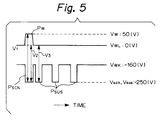
- FIG. 5 shows the waveforms and is useful for understanding the potential shown in FIG. 2.
- the voltage appearing between the display discharge anode and the cathode in the display cell 4 mn during the non-writing becomes equal to the voltage appearing during the sustain discharge.
- This fails to provide a degree of freedom in setting up the width and amplitude of the write pulse Pw.
- it is difficult to conduct an adjustment, in other words, it is difficult to ensure a sufficient memory margin, which means the range of the sustain discharge voltage with which a normal sustain discharge can be obtained.
- the high level of potential Vw of the write pulse Pw is 50 volts (V)
- the low level of potential V WL of the write pulse Pw is zero volts
- the bias potential Vb of the cathodes 31-3 M is -160V
- the low level of potential Vscn of the scan pulse Pscn is -255V
- the low level of potential Vsus of the sustain pulse Psus is -255V
- voltage V1 between the display discharge anodes I n and the cathode 3 m in the display cell 4 mn is 305V during the writing.
- Voltage V2 during the non-writing is 255V
- voltage V3 during the sustain discharge by the sustain pulse Psus is also 255V.
- FIG. 6 shows the waveforms and is useful for understanding how the potential shown in FIG. 4 is set up.
- the potential Vscn of the scan pulse Pscn and the potential Vsus of the sustain pulse Psus are different from each other in potential level.
- the voltage V1 during the writing, which is to be applied to the display discharge anode I n is set up to 305V
- the voltage V2 during the non-writing is set up to the maximum voltage 220V which involves no formation of the discharge during the non-writing.
- the high level of potential Vw of the write pulse Pw is 305 V
- the low level of potential V WL of the write pulse Pw is 220V.
- the low level of potential Vsus of the sustain pulse Psus is -35V, which is equal to 220V-255V.
- the bias potential V BK of the cathode is selected in such a manner that the voltage V6 applied to the display cell is 220V, which is the maximum voltage involving no formation of the discharge, so as not to establish the discharge in combination of the bias potential V BK of the cathode with the potential of the write pulse Pw.
- the bias potential V BK is given by 85V, which is equal to 305V-220V.
- voltage V4 for the auxiliary discharge is given by 300V
- a potential 300V is applied to the auxiliary cathode in timed with the scan pulse Pscn.
- the voltage V5 applied to the auxiliary discharge cell 5 mj is set up to 230V, which is the maximum voltage involving no formation of the discharge. That means the low level of potential V SAL of the auxiliary pulse P SA is given by 195V, which is equal to -35V+230V.
- the set-up of the voltages as described above makes it possible to set up the voltages V1 and V2 for writing separately from the voltage V3 for sustaining.
- the memory margin characteristics of the respective display cells 4 mn are not harmed.
- the set-up of the voltages in the manner as described above needs high amplitudes of the pulses such that the amplitude on the cathode 3 m is 120V, the amplitude on the display discharge anode 1 n is 85V, and the amplitude on the auxiliary cathode 2 j is 105V. This makes it difficult to incorporate the peripheral circuits of the display device into an integrated circuit.
- a method of memory driving a plasma display panel which comprises a gro up of display electrodes constituted of a plurality of linear electrodes arranged, a group of scan electrodes constituted of a plurality of linear electrodes arranged in such a manner that said group of scan electrodes is placed over against said group of display electrodes and is perpendicular to said group of display electrodes, a discharge gas being enclosed between said group of display electrodes and said group of scan electrodes, and a plurality of display cells disposed on intersections of the respective display electrodes and the respective scan electrodes, each of said plurality of display cells emitting light through a discharge between an associated display electrode and an associated scan electrode, comprises the steps of: sequentially applying scan pulses to the scan electrodes and, following the scan pulse, applying a train of sustain pulses to each of the scan electrodes during a predeteminend period of time; applying a non-write pulse to said group of display electrodes in synchronism with the scan pulse,
- said group of display electrodes and said group of scan electrodes may be adopted as a group of anodes and a group of cathodes, respectively, and said non-write pulse may be a binary signal having a high level corresponding to a turn-on level with which the write discharge is initiated, and a low level corresponding to a turn-off level for the non-display.
- said group of display electrodes and said group of scan electrodes may be adopted as a group of cathodes and a group of anodes, respectively, and said non-write pulse may be a binary signal having a low level corresponding to a turn-on level with which the write discharge is initiated, and a high level corresponding to a turn-off level for the non-display.
- FIGS. 7 and 8 schematically show a construction of a direct-current plasma display panel (DC-PDP) according to an embodiment of the present invention.
- DC-PDP direct-current plasma display panel
- the like parts are denoted by the same reference numerals as those of FIG. 1.
- the embodiment of a DC-PDP in accordance with the invention comprises display electrodes of display discharge anodes 11-1 N in which a plurality of linear electrodes are arranged, auxiliary electrodes or auxiliary anodes 21-2 J and scan electrodes or cathodes 31-3 M which intersect perpendicularly to the display discharge anodes 11-1 N and the auxiliary anodes 21-2 J , where N, J and M are natural numbers.
- the respective intersections of the display discharge anodes 11-1 N and the cathodes 31-3 M form associated display cell 4 mn , where 1 ⁇ n ⁇ N , and 1 ⁇ m ⁇ M . Further, the respective intersections of the auxiliary anodes 21-2 J and the cathodes 31-3 M form also associated auxiliary discharge cell 5 mj , where 1 ⁇ j ⁇ J .
- the respective display cells 4 mn are spatially isolated from each other with barriers 6, and are each coupled with the adjacent auxiliary cell through a priming slit 7.
- the display discharge anodes 11-1 N and the auxiliary anodes 21-2 J are formed on a front plate 8, and the cathodes 31-3 M are formed on a rear plate 9 located over against the front plate 8.
- a discharge gas such as a mixing gas of helium and xenon, is enclosed between the front and rear plates 8 and 9.
- a phosphor layer is disposed on each display cell 4 mn .
- the display discharge anodes 11-1 N , the auxiliary anodes 21-2 J and the cathodes 31-3 M are connected in a fashion similar to that of FIG. 1, so that the display cells 4 mn are driven on a memory basis.
- the display discharge anodes 11-1 N serve as the display electrodes, to which pulses each representative of information to be displayed and directed to the associated display cell 4 mn are applied from the anode drive circuits 111-11 N .
- the cathodes 31-3 M serve as the scan electrodes, to which scan pulses are applied from the cathode drive circuits 131-13 M .
- FIG. 9 shows waveforms useful for understanding a memory drive scheme of the DC-PDP according to the embodiment of the present invention.
- FIG. 9 shows an auxiliary anode signal S which is applied in common to the respective auxiliary anodes 21-2 J , display anode signals A1, A2,...,A N which are applied to the display discharge anodes 11, 12, ...,1 N , and cathode signals K1, K2,...,K M which are applied to the cathodes 31, 32,...,3 M .
- the cathode signals K1, K2,...,K M comprise each a scan pulse P SCN and the subsequent sustain pulses P SUS which appear during a certain period of time and are each different from the scan pulse P SCN in phase.
- the cathode signals K1, K2,...,K M are sequentially applied to the cathodes 31, 32,...,3 M , respectively.
- the display anode signals A1, A2,...,A N are each a binary signal comprising a non-write pulse P NW representative of information to be displayed and are applied to the display discharge anodes 11, 12,...,1 N , respectively.
- the non-write pulse P NW takes its low level, i.e. OFF level, in synchronism with the scan pulse P SCN only when a write discharge on the display cell 4 mn is not conducted, and takes its high level, i.e. ON level, during the remaining period of time.
- the auxiliary anode signal S serves to apply an auxiliary discharge pulse P SA to the auxiliary anodes 21-2 J in synchronism with the scan pulse P SCN .
- FIG. 10 shows waveforms useful for understanding the potential set-up shown in FIG. 9.
- the bias potential V BA of the display discharge anode 1 n is set up to 305V so that the write voltage V11 to be applied to the display cell 4 mn becomes 305V.
- the low level of potential V Nw of the non-write pulse P Nw is also set up to 220V so that the voltage V12 during non-writing is 220V which is the maximum voltage involving no discharge.
- the sustain voltage on the display cell 4 mn is to be 255V corresponding to V16
- the low level of potential V SUS of the sustain pulse P SUS is set up to 50V, which is equal to 305V-255V.
- the bias potential V Bk of the cathode 3 m is set up to 85V, equal to 305V-220V, so that voltage V13 between the bias potential V Bk of the cathode 3 m and the bias potential V BA of the display discharge anode 1 n is 220V, for example, which is the maximum voltage involving no discharge. Since the auxiliary discharge voltage V14 is 300V, the high level of potential V SA of the auxiliary pulse P SA is set up to be 300V in timed with the scan pulse P SCN .
- the bias potential V BS of the auxiliary node signal S is set up to 280V, equal to 230V+50V, so that the voltage V15 applied to the auxiliary cell 5 mj is 230V which is the maximum voltage involving no discharge.
- the scan pulses P SCN having the pulse width ⁇ SCN of 1.5 ⁇ s are supplied every 4 ⁇ s to the cathodes 31, 32,...,3 M functioning as the scan electrodes.
- the supply of the scan pulses P SCN to the cathodes 31, 32,...,3 M is sequentially conducted with time lag.
- the auxiliary discharge pulses P SA having the pulse width ⁇ SA of 1.5 ⁇ s, which are synchronized with the scan pulses P SCN are applied to the auxiliary anodes 21-2 J every 4 ⁇ s, so that the auxiliary discharge in the auxiliary discharge cell 5 mj is shifted together with the scan pulse P SCN .
- the sustain pulses P SUS having the pulse width ⁇ SUS of 1.5 ⁇ s are applied to each of the cathodes 31, 32,...,3 M during a certain period of time at a timing not overlapping the scan pulse P SCN . Since the potential V SA of the auxiliary anodes 21-2 J is 280V during a period of time in which the sustain pulse P SUS is applied, the voltage applied to the auxiliary discharge cell 5 mj is 230V, corresponding to V BS -V SUS . Thus, it does not happen that the auxiliary discharge cell 5 mj involves a discharge in this timing.
- the bias voltage V BK of the cathodes 31, 32,...,3 M is 85V during a period of time in which none of the scan pulse P SCN and the sustain pulse P SUS is applied thereto. If the information to be displayed is not representative of the non-display, then the potential of the n-th column of display discharge anode 1 n is the bias voltage V BA , which is 305V in this instance.
- the potential of the m-th row of cathode 3 m is the low level of potential V SCN , i.e. 0V
- the voltage is 305V between the display discharge anode 1 n and the cathode 3 m , so that the write discharge is initiated on the display cell 4 mn .
- the ions, excited atoms and the like are diffused from the m-th row of auxiliary discharge cell 5 mj , which discharges near the display cell 4 mn , through the priming slit 7 as shown in FIG. 7 to the display cell 4 mn .
- the write discharge is immediately formed with help of the ions, the excited atoms and the like.
- a non-write pulse P NW having the pulse width ⁇ NW of 1.5 ⁇ s is applied to the n-th column of display discharge anode 1 n in synchronism with the scan pulse P SCN applied to the cathode 3 m .
- the voltage applied to the display cell 4 mn is 220V, corresponding to V NW -V SCN , and does not reach the voltage which forms the discharge.
- the write discharge to the display cell 4 mn is not accomplished.
- a gaseous discharge is provided with such characteristics that ions and excited atoms, which emanate by the discharging, are gradually decreased after the discherging are terminated, and the presence of the ions and excited atoms is prone to involve a re-discharge. Consequently, for example, if a write discharge is formed on the display cell 4 mn , then the discharge can be maintained on the display cell 4 mn , in spite of the voltage 255V lower than the write voltage 305V, in timed with the sustain pulse P SUS which is supplied following the scan pulse P SCN . The display cell 4 mn sustains an intermittent discharge by the sustain pulse P SUS . Thus, the memory drive is implemented.
- the potential of the display discharge anode 1 n is set to the bias potential V BA corresponding to the high level of the non-write pulse P Nw
- the low level of potential V SCN of the scan pulse P SCN is applied to the cathode 3 m to form the write discharge
- the sustain discharge is conducted in the form of pulses with a voltage between the low level of potential V SUS in the subsequent sustain pulse P SUS and the bias potential V BA .
- the low level of potential V NW equivalent to the OFF level of the non-write pulse P NW , is applied to the display discharge anode 1 n in synchronism with the scan pulse P SCN applied to the cathode 3 m .
- the scan pulse P SCN applied to the cathode 3 m .
- decrement of the potential V NW of the OFF level of the non-write pulse P NW makes it possible to set up the voltage V12 for non-writing to a value which is sufficiently lower than the voltage V ⁇ of the V-segment of the I-V characteristic shown in FIG. 3 concerning the display cell 4 mn .
- the voltage V16 for conducting the sustain discharge, as shown in FIG. 10 is not varied. In other words, it is possible to establish a sufficient memory margin for the respective display cells.
- the display anode signals applied to the display discharge anodes 11-1 N are each a binary signal.
- the use of the binary signals make it possible to simplify the drive circuits in structure.
- the amplitudes of the auxiliary anode signal S, the display anode signals A1, A2,...,A N and the cathode signals K1, K2,...,K M are reduced, as 20V, 85V and 85V, respectively, as shown in FIG. 10, in comparison with the prior art scheme.
- reducing the amplitude of the respective signals makes it possible to provide a lower power consumption of the DC-PDP in comparison with the prior art scheme.
- FIG. 11 is a schematic block diagram of the DC-PDP and its drive circuit implementing the memory drive scheme according to the present invention.
- the embodiment shown in FIG. 11 includes a display anode drive circuit 11 which comprises the anode drive circuits 111-11 N which are connected to the display discharge anodes 11-1 N of the DC-PDP 10, respectively.
- a cathode drive circuit 13 comprising the cathode drive circuits 131-13 M which are connected to the cathodes 31-3 M , respectively.
- an auxiliary anode drive circuit 12 is connected to the auxiliary anodes 21-2 J .
- the display anode drive circuit 11 is constituted of, for example, a shift register, a latch circuit, an AND gate circuit and a high voltage C-MOS driver.
- the auxiliary anode drive circuit 12 is constituted of, for example, a high voltage C-MOS driver.
- the cathode drive circuit 13 is constituted of a scan pulse generating unit which comprises a shift register for scan pulse, an AND gate circuit and a high voltage N-MOS driver, and a sustain pulse generating unit which comprises a shift register for sustain pulse, an AND gate circuit, a high voltage P-MOS driver and a high voltage N-MOS driver.
- FIG. 12 shows waveforms useful for understanding the memory drive scheme of a DC-PDP according to an alternative embodiment of the present invention.
- the display electrodes 11-1 N are used as the display discharge anodes to which the non-write pulse P Nw is applied as information to be displayed
- the scan electrodes 31-3 M are used as the cathodes to which the scan pulse P SCN and the sustain pulse P SUS are applied to perform the memory drive of the DC-PDP.
- the display electrodes 11-1 N are used as the display discharge cathodes to which the non-write pulse which offers a high level for non-writing is applied, and the scan electrodes 31-3 M are used as the anodes to which the scan pulse P SCN and the sustain pulse P SUS are applied to perform the memory drive on the DC-PDP.
- FIG. 12 shows a display cathode signal K n which is supplied to the display discharge cathodes 11, 12,...,1 N , and anode signals A1, A2,...,A M which are supplied to the anodes 31, 32,...,3 M , respectively.
- the high level of potential V SCNH of the scan pulse P SCN having its pulse width of 1.5 ⁇ s applied to the anodes 31, 32,..., 3 M is set up to 305V.
- the sustain pulses P SUS which are supplied to the anodes 31, 32,...,3 M , have also the pulse width of 1.5 ⁇ s, the high level of potential V SUSH of the sustain pulse P SUS is set up to 255V.
- the bias potential V BA 220V is applied to the anodes 31, 32,..,3 M .
- Applied to the display discharge cathodes 11, 12, ...,1 N is a non-write pulse P NW having its pulse width of 1.5 ⁇ s dependent upon the information to be displayed.
- the non-write pulse P NW shown in FIG. 12 has its low level corresponding to a turn-on level with which the write discharge is initiated depending upon information to be displayed, and its high level corresponding to a turn-off level not displaying.
- the low level of the potential of the non-write pulse P NW is set up to the bias potential V BK , i.e. zero volts, and the high level of the potential V NWH is set up to 85V.
- the scan pulses P SCN having the pulse width ⁇ SCN of 1.5 ⁇ s are supplied every 4 ⁇ s to the anodes 31, 32,...,3 M serving as the scan electrodes.
- the supply of the scan pulses P SCN to the anodes 31, 32,...,3 M is sequentially conducted with time lag.
- the sustain pulses P SUS having the pulse width ⁇ SUS of 1.5 ⁇ s are applied to each of the anodes 31, 32,...,3 M during a certain period of time at the timing not overlapping the scan pulse P SCN .
- the bias voltage V BA of the anodes 31, 32,...,3 M is 220V during a period of time in which none of the scan pulse P SCN and the sustain pulse P SUS is applied thereto.
- a non-write pulse P NW having its pulse width ⁇ NW of 1.5 ⁇ s is applied to the n-th column of display discharge cathode 1 n in synchronism with the scan pulse P SCN applied to the anode 3 m .
- the voltage applied to the display cell 4 mn is 220V, corresponding to V SCNH -V NWH , and does not reach the voltage which forms the discharge.
- a write discharge to the display cell 4 mn is not formed.
- a write discharge is formed on the display cell 4 mn , it can be maintained on the display cell 4 mn , in spite of the voltage 255V, corresponding to V SUSH -V BK , lower than the write voltage 305V, at the timing of the sustain pulse P SUS which is supplied following the scan pulse P SCN .
- the display cell 4 mn sustains an intermittent discharge by the sustain pulse P SUS , so that the memory drive is implemented.
- the sustain pulse P SUS applied following the scan pulse P SCN does not serve to form the discharge.
- the scan electrodes 31, 32,..., 3 M are used as the anodes to which the scan pulse P SCN and the sustain pulse P SUS are applied, and the display electrodes 11, 12,...,1 N are used as the cathodes to which the non-write pulse P Nw is applied.
- the display electrodes 11, 12,...,1 N are used as the cathodes to which the non-write pulse P Nw is applied.
- the display anode signals applied to the display discharge cathodes 11-1 N are binary signals.
- the use of the binary signals make it possible to simplify the cathode drive circuits 111-11 N in structure.
- the amplitudes of the anode signals A1, A2,...,A N and the display cathode signals K1, K2,...,K M are reduced, as 85V and 85V, respectively. This facilitates the anode drive circuit 13, the cathode drive circuit 11 and the like to be fabricated into an integrated circuit.
- reducing the amplitude of the respective signals makes it possible to provide a lower power consuption of the DC-PDP in comparison with the prior art scheme.
- the scan electrodes are fed with the train of scan pulses and sustain pulses with the display electrodes supplied with the non-write pulse, which offers the turn-off level only when information to be displayed and applied to the display cells is of non-display, and the write discharge commences for the display cells, to which information to be displayed is not of non-display, in response to the scan pulse and dependent upon the turn-on levels other than the turn-off level of the non-write pulse, with the discharge sustained in response to the train of sustain pulses and dependent upon the turn-on level of the display electrode.
- the writing voltage independently of the sustain voltage for the display cells in the PDP, thereby ensuring a sufficient memory margin.
- the invention it is possible to reduce the amplitude of the signals which are supplied to the display electrodes, the scan electrodes and the auxiliary electrodes, thereby implementing a lower power consumption of the PDP, and in addition facilitating the peripheral circuits to be placed in an integrated circuit.
- the group of display electrodes and the group of scan electrodes are adopted as the group of anodes and the group of cathodes, respectively.
- the non-write pulse is a binary signal having its high and low levels.
- the high level corresponds to a turn-on level with which the write discharge is initiated.
- the low level corresponds to a turn-off level for not-displaying.
- the group of display electrodes and the group of scan electrodes may be adopted as the group of cathodes and the group of anodes, respectively.
- the non-write pulse is a binary signal having its high and low levels.
- the low level corresponds to a turn-on level with which the write discharge is initiated.
- the high level corresponds to a turn-off level for not-displaying.
- this feature makes it possible to ensure a sufficient memory margin and also to facilitate the PDP to consume lower power and the peripheral circuits to be placed in an integrated circuit. Further, it is possible to simplify in structure the cathode drive circuit supplying non-write pulses.
Landscapes
- Engineering & Computer Science (AREA)
- Physics & Mathematics (AREA)
- Plasma & Fusion (AREA)
- Computer Hardware Design (AREA)
- General Physics & Mathematics (AREA)
- Theoretical Computer Science (AREA)
- Control Of Indicators Other Than Cathode Ray Tubes (AREA)
- Control Of Gas Discharge Display Tubes (AREA)
- Transforming Electric Information Into Light Information (AREA)
Applications Claiming Priority (2)
| Application Number | Priority Date | Filing Date | Title |
|---|---|---|---|
| JP6262459A JP3062406B2 (ja) | 1994-10-26 | 1994-10-26 | 直流型気体放電パネルのメモリ駆動方法 |
| JP262459/94 | 1994-10-26 |
Publications (2)
| Publication Number | Publication Date |
|---|---|
| EP0709820A2 true EP0709820A2 (fr) | 1996-05-01 |
| EP0709820A3 EP0709820A3 (fr) | 1997-01-15 |
Family
ID=17376085
Family Applications (1)
| Application Number | Title | Priority Date | Filing Date |
|---|---|---|---|
| EP95116050A Withdrawn EP0709820A3 (fr) | 1994-10-26 | 1995-10-11 | Méthode de commande avec effet mémoire d'un panneau d'affichage à plasma en utilisant des tensions d'écriture et d'entretien indépendantes |
Country Status (4)
| Country | Link |
|---|---|
| US (1) | US5677600A (fr) |
| EP (1) | EP0709820A3 (fr) |
| JP (1) | JP3062406B2 (fr) |
| TW (1) | TW273614B (fr) |
Cited By (2)
| Publication number | Priority date | Publication date | Assignee | Title |
|---|---|---|---|---|
| EP0817161A1 (fr) * | 1996-06-26 | 1998-01-07 | Oki Electric Industry Co., Ltd. | Méthode de commande avec effet mémoire d'un panneau d'affichage à plasma en champ continu |
| CN101630479B (zh) * | 2008-06-25 | 2012-09-26 | 索尼株式会社 | 显示设备 |
Families Citing this family (7)
| Publication number | Priority date | Publication date | Assignee | Title |
|---|---|---|---|---|
| JPH10247456A (ja) * | 1997-03-03 | 1998-09-14 | Fujitsu Ltd | プラズマディスプレイパネル、プラズマディスプレイ装置、及びプラズマディスプレイパネルの駆動方法 |
| US6369781B2 (en) * | 1997-10-03 | 2002-04-09 | Mitsubishi Denki Kabushiki Kaisha | Method of driving plasma display panel |
| KR100346376B1 (ko) * | 1999-04-15 | 2002-08-01 | 삼성에스디아이 주식회사 | 플라즈마 표시 패널의 구동 장치 |
| US8853696B1 (en) | 1999-06-04 | 2014-10-07 | Semiconductor Energy Laboratory Co., Ltd. | Electro-optical device and electronic device |
| TW543206B (en) * | 1999-06-28 | 2003-07-21 | Semiconductor Energy Lab | EL display device and electronic device |
| KR100445418B1 (ko) * | 2001-10-09 | 2004-08-25 | 삼성에스디아이 주식회사 | 플라즈마 디스플레이 패널의 구동 방법 |
| US20060227253A1 (en) * | 2005-04-07 | 2006-10-12 | Kim Nam J | Plasma display apparatus and driving method thereof |
Family Cites Families (7)
| Publication number | Priority date | Publication date | Assignee | Title |
|---|---|---|---|---|
| US4097856A (en) * | 1976-10-04 | 1978-06-27 | International Business Machines Corporation | Gas panel single ended drive systems |
| JPS60221796A (ja) * | 1984-04-18 | 1985-11-06 | 富士通株式会社 | ガス放電パネルの駆動方法 |
| US4692665A (en) * | 1985-07-05 | 1987-09-08 | Nec Corporation | Driving method for driving plasma display with improved power consumption and driving device for performing the same method |
| JP3026317B2 (ja) * | 1991-10-30 | 2000-03-27 | 松下電子工業株式会社 | 気体放電型表示装置の駆動方法 |
| KR940007245B1 (ko) * | 1991-11-04 | 1994-08-10 | 삼성전관 주식회사 | 플라즈마 표시소자 |
| JP3078114B2 (ja) * | 1992-06-26 | 2000-08-21 | 日本放送協会 | 気体放電表示パネルの駆動方法および駆動装置 |
| JP2772753B2 (ja) * | 1993-12-10 | 1998-07-09 | 富士通株式会社 | プラズマディスプレイパネル並びにその駆動方法及び駆動回路 |
-
1994
- 1994-10-26 JP JP6262459A patent/JP3062406B2/ja not_active Expired - Fee Related
-
1995
- 1995-07-25 TW TW084107722A patent/TW273614B/zh active
- 1995-10-11 EP EP95116050A patent/EP0709820A3/fr not_active Withdrawn
- 1995-10-26 US US08/548,668 patent/US5677600A/en not_active Expired - Lifetime
Cited By (3)
| Publication number | Priority date | Publication date | Assignee | Title |
|---|---|---|---|---|
| EP0817161A1 (fr) * | 1996-06-26 | 1998-01-07 | Oki Electric Industry Co., Ltd. | Méthode de commande avec effet mémoire d'un panneau d'affichage à plasma en champ continu |
| US5920295A (en) * | 1996-06-26 | 1999-07-06 | Oki Electric Industry Co., Ltd. | Memory drive system of a DC type of plasma display panel |
| CN101630479B (zh) * | 2008-06-25 | 2012-09-26 | 索尼株式会社 | 显示设备 |
Also Published As
| Publication number | Publication date |
|---|---|
| US5677600A (en) | 1997-10-14 |
| JP3062406B2 (ja) | 2000-07-10 |
| TW273614B (en) | 1996-04-01 |
| EP0709820A3 (fr) | 1997-01-15 |
| JPH08123363A (ja) | 1996-05-17 |
Similar Documents
| Publication | Publication Date | Title |
|---|---|---|
| KR100917373B1 (ko) | 플라즈마 디스플레이 패널의 구동 방법 | |
| US6483251B2 (en) | Method of driving plasma display | |
| KR20000035306A (ko) | 플라즈마 디스플레이 패널과 구동장치 및 방법 | |
| EP0709820A2 (fr) | Méthode de commande avec effet mémoire d'un panneau d'affichage à plasma en utilisant des tensions d'écriture et d'entretien indépendantes | |
| US6628251B1 (en) | Method capable of establishing a high contrast on a PDP | |
| JP3628195B2 (ja) | プラズマディスプレイパネル装置 | |
| US5739799A (en) | Method of memory-driving a DC gaseous discharge panel and circuitry therefor | |
| JP3787713B2 (ja) | プラズマディスプレイ装置 | |
| JP3078114B2 (ja) | 気体放電表示パネルの駆動方法および駆動装置 | |
| US5920295A (en) | Memory drive system of a DC type of plasma display panel | |
| US20060022602A1 (en) | Method and apparatus for driving plasma display panel | |
| KR100476149B1 (ko) | 플라즈마디스플레이패널 및 그 구동방법 | |
| JP3638106B2 (ja) | プラズマディスプレイパネルの駆動方法 | |
| EP0652458A1 (fr) | Dispositif d'affichage à cristaux liquides adressés par plasma utilisable avec une séquence de ligne optimale par temporisation | |
| JPH07210113A (ja) | プラズマディスプレイパネルの駆動方法 | |
| US20020180667A1 (en) | Method for operating plasma display panel | |
| JP3402272B2 (ja) | プラズマディスプレイパネル駆動方法 | |
| JPH1011020A (ja) | プラズマディスプレイパネルの駆動方法 | |
| KR100382437B1 (ko) | 플라즈마 표시 소자의 구동방법 | |
| JP2889058B2 (ja) | 気体放電表示装置の駆動方法 | |
| JPH07129119A (ja) | 気体放電表示装置の駆動方法 | |
| JPH07104658B2 (ja) | プラズマ表示装置の駆動方法 | |
| JPH07152342A (ja) | 気体放電発光装置の駆動方法 | |
| JPH09297558A (ja) | 気体放電パネルの補助セル駆動方法 |
Legal Events
| Date | Code | Title | Description |
|---|---|---|---|
| PUAI | Public reference made under article 153(3) epc to a published international application that has entered the european phase |
Free format text: ORIGINAL CODE: 0009012 |
|
| AK | Designated contracting states |
Kind code of ref document: A2 Designated state(s): DE FR GB |
|
| RIN1 | Information on inventor provided before grant (corrected) |
Inventor name: KOBAYASHI, YOSHIHIKO, C/O OKI ELECTRIC IND. CO LT Inventor name: TEROUCHI, YUJI, C/O OKI ELECTRIC IND. CO., LTD. Inventor name: TAKAHASHI, ATSUSHI,C/O OKI ELECTRIC IND. CO., LTD. |
|
| PUAL | Search report despatched |
Free format text: ORIGINAL CODE: 0009013 |
|
| AK | Designated contracting states |
Kind code of ref document: A3 Designated state(s): DE FR GB |
|
| 17P | Request for examination filed |
Effective date: 19970311 |
|
| STAA | Information on the status of an ep patent application or granted ep patent |
Free format text: STATUS: THE APPLICATION HAS BEEN WITHDRAWN |
|
| 18W | Application withdrawn |
Withdrawal date: 19990209 |