EP0709874B1 - Diagnostische Scheibe - Google Patents
Diagnostische Scheibe Download PDFInfo
- Publication number
- EP0709874B1 EP0709874B1 EP95117154A EP95117154A EP0709874B1 EP 0709874 B1 EP0709874 B1 EP 0709874B1 EP 95117154 A EP95117154 A EP 95117154A EP 95117154 A EP95117154 A EP 95117154A EP 0709874 B1 EP0709874 B1 EP 0709874B1
- Authority
- EP
- European Patent Office
- Prior art keywords
- grid
- discriminator
- annular insulator
- wafer
- placebo
- Prior art date
- Legal status (The legal status is an assumption and is not a legal conclusion. Google has not performed a legal analysis and makes no representation as to the accuracy of the status listed.)
- Expired - Lifetime
Links
Images


Classifications
-
- H—ELECTRICITY
- H01—ELECTRIC ELEMENTS
- H01J—ELECTRIC DISCHARGE TUBES OR DISCHARGE LAMPS
- H01J37/00—Discharge tubes with provision for introducing objects or material to be exposed to the discharge, e.g. for the purpose of examination or processing thereof
- H01J37/32—Gas-filled discharge tubes
- H01J37/32917—Plasma diagnostics
- H01J37/32935—Monitoring and controlling tubes by information coming from the object and/or discharge
-
- H—ELECTRICITY
- H10—SEMICONDUCTOR DEVICES; ELECTRIC SOLID-STATE DEVICES NOT OTHERWISE PROVIDED FOR
- H10P—GENERIC PROCESSES OR APPARATUS FOR THE MANUFACTURE OR TREATMENT OF DEVICES COVERED BY CLASS H10
- H10P74/00—Testing or measuring during manufacture or treatment of wafers, substrates or devices
- H10P74/20—Testing or measuring during manufacture or treatment of wafers, substrates or devices characterised by the properties tested or measured, e.g. structural or electrical properties
- H10P74/207—Electrical properties, e.g. testing or measuring of resistance, deep levels or capacitance-voltage characteristics
-
- H—ELECTRICITY
- H10—SEMICONDUCTOR DEVICES; ELECTRIC SOLID-STATE DEVICES NOT OTHERWISE PROVIDED FOR
- H10P—GENERIC PROCESSES OR APPARATUS FOR THE MANUFACTURE OR TREATMENT OF DEVICES COVERED BY CLASS H10
- H10P74/00—Testing or measuring during manufacture or treatment of wafers, substrates or devices
- H10P74/27—Structural arrangements therefor
-
- H—ELECTRICITY
- H01—ELECTRIC ELEMENTS
- H01J—ELECTRIC DISCHARGE TUBES OR DISCHARGE LAMPS
- H01J2237/00—Discharge tubes exposing object to beam, e.g. for analysis treatment, etching, imaging
- H01J2237/244—Detection characterized by the detecting means
- H01J2237/24485—Energy spectrometers
-
- H—ELECTRICITY
- H01—ELECTRIC ELEMENTS
- H01J—ELECTRIC DISCHARGE TUBES OR DISCHARGE LAMPS
- H01J2237/00—Discharge tubes exposing object to beam, e.g. for analysis treatment, etching, imaging
- H01J2237/245—Detection characterised by the variable being measured
- H01J2237/24507—Intensity, dose or other characteristics of particle beams or electromagnetic radiation
Definitions
- the present invention refers to a diagnostic wafer, and particularly to a diagnostic wafer for semiconductor wafer processing systems.
- Ion current flux and ion energy are important parameters of a plasma contained by a reaction chamber within a semiconductor processing system. These parameters define the effectiveness of the semiconductor wafer processing system in processing a wafer. Specifically, the ion current flux affects the uniformity of the etch process and indicates potential damage to a wafer. Additionally, ion energy affects selectivity of the etch, etch rate uniformity and residue control. Since these parameters are so important to the etch process, the measurement of both ion current and ion energy at a given location within the chamber is important to characterizing the effectiveness of the plasma in processing a wafer.
- an ion current probe similar to a Langmuir probe, is used.
- a placebo wafer i.e., an anodized aluminum disk having the same size and shape as a semiconductor wafer.
- the placebo wafer is then positioned within a semiconductor processing system in a similar location as a semiconductor wafer would typically be located.
- the ion current probes are biased negatively to collect ions from the plasma. Consequently, an electric current is produced in a wire attaching the probe to a current meter.
- the measured current is indicative of the number of ions incident upon the current probe at that location on the placebo wafer.
- the ion currents measured at each individual current probe are combined to estimate the ion current distribution over the surface of the placebo wafer. This current distribution is indicative of the ion current flux within the plasma.
- an ion energy analyzer is generally imbedded into a support structure for the semiconductor wafer, e.g., such support structures are known as wafer chucks, susceptors, or wafer pedestals.
- An ion energy analyzer is a well known device for determining the energy properties of ions within a plasma. For a detailed description of an ion energy analyzer, see R.L. Stenzel et al., "Novel Directional Ion Energy Analyzer", Rev. Sci. Instrum. 53(7), July 1982, pp. 1027-1031.
- a traditional ion energy analyzer contains a metallic collector, a control grid, and a floating grid, all formed into a cylindrical stack where the collector and each grid are separated by a ceramic insulating washer.
- the collector is a negatively biased metallic disk.
- the negative bias repels electrons from the collector and attracts ions to the collector.
- the control grid is positively biased such that ions with energies that do not exceed the positive bias are rejected by the analyzer.
- the control grid is used to select ions for collection that have energy levels greater than a specified energy level and reject all others.
- the unbiased (floating) grid is either a mesh screen or a micro-channel plate, being unbiased, simulates the surface of a semiconductor wafer.
- the ion energy analyzer imbedded in the pedestal is either used to measure the ion energy prior to having a wafer placed upon the pedestal or a specially designed wafer, having a hole to expose the energy analyzer to the plasma, is placed upon the pedestal.
- ions having energies exceeding the control grid bias are collected by the collector plate and create an electrical current in an ampere-meter connected to the collector plate.
- the energy of the ions in the plasma is determined by adjusting the control grid bias and monitoring the current measured by the ampere-meter.
- the prior art teaches separately using current probes on a placebo wafer and an ion energy analyzer imbedded in a wafer pedestal. As such, to determine both ion current and ion energy, first the ion current is measured and then the ion energy is measured, or vice versa. Due to the necessity to conduct two sequential measurements, the duration of plasma test is much longer than each of the measurements taken singly. Furthermore, since the current and energy measurements are separated in time, such measurements can be inaccurate.
- the present invention provides, on a single placebo wafer, one or more ion current probes with one or more ion energy analyzers.
- the invention relates to test and measurement apparatus for semiconductor wafer processing system and, more particularly, to a composite diagnostic wafer for measuring both ion energy and ion current at various locations on the diagnostic wafer during plasma generation by a semiconductor wafer processing system.
- the invention specifically refers to a single diagnostic wafer combining both one or more ion current probes with one or more ion energy analyzers to facilitate substantially simultaneous ion current and energy measurement within a semiconductor wafer processing system.
- the present invention is a composite diagnostic wafer containing a placebo wafer fabricated of an anodized aluminum disk having substantially the same dimensions as a semiconductor wafer.
- the disk has affixed to one surface, or imbedded within one surface, one or more ion current probes and one or more ion energy analyzers.
- measurement instrumentation connected to the analyzer(s) and probes(s) determines both ion current and ion energy at various locations upon the wafer. Consequently, both ion current and ion energy are measured substantially simultaneously and at substantially the same location on the placebo wafer.
- a plasma can be fully characterized at a plurality of locations on the placebo wafer.
- each analyzer is optionally fitted with a micro-channel plate rather than a conventional floating grid.
- the thickness of the plate and the length of the channels define the geometric filtering characteristics of the plate.
- FIG. 1 depicts a top-plan view of a composite diagnostic wafer 100 containing placebo wafer 102 with both an ion energy analyzer 104 m (m being an integer value greater than or equal to 1) and an ion current probe 106 n (n being an integer value greater than or equal to 1) affixed to a surface of the placebo wafer.
- FIG. 2 is a cross-sectional view of the composite diagnostic wafer 100 along line 2-2 shown in FIG. 1. To best understand the invention, the reader should simultaneously consult both FIGS. 1 and 2.
- the placebo wafer 102 is an anodized aluminum disk having dimensions equivalent to a semiconductor wafer that it replaces within a semiconductor processing system.
- the diameter and thickness of the placebo wafer are the same as a semiconductor wafer such that the bottom surface of the placebo wafer can be mounted to a chuck or a wafer pedestal within the processing system.
- the chuck then supports the placebo wafer within the processing system in a location that ensures that the placebo wafer experiences the same ion bombardment from a plasma as a semiconductor wafer would experience in that same location.
- any measuring instrumentation attached to the placebo wafer measures the environment within the processing system as it would be generated proximate the semiconductor wafer.
- One illustrative semiconductor wafer processing system that can utilize the present invention is a model Centura HDP metal etch system manufactured by Applied Materials, Inc. of Santa Clara, California.
- the placebo wafer 102 supports a plurality of energy analyzers 104 m and a plurality of current probes 106 n coaxially aligned with the energy analyzers.
- the analyzers and probes are positioned in an array such that the properties of the plasma can best be determined over the entire surface of the wafer.
- the overall height (thickness) of the composite diagnostic wafer (placebo wafer, energy analyzers and current probes) is approximately 2.54 - 3.81 mm (100 to 150 mils).
- the placebo wafer may optionally contain one or more extensions or wings that extend from the circumference of the placebo wafer (one extension is shown as dashed area 110 in FIG. 1). These extensions can be used to support current probes and/or energy analyzers at locations that are outside the diameter of the wafer, e.g., at locations near the walls of the reaction chamber.
- a plurality of disk-like insulators 108 typically fabricated from a ceramic material. Each insulator is approximately 5 to 20 mils thick.
- a plurality of analyzers are fabricated by attaching, using an adhesive, a collector 200 for each analyzer 106 to the placebo wafer 102.
- Each collector 200 is a disk of conductive material such as tungsten or stainless steel. The collectors are individually connected by wires (not shown) to a voltage source for biasing the collectors with an adjustable negative potential.
- Atop the collectors is positioned a disk-like insulator 202 containing apertures 204.
- Each of the apertures has a diameter that is slightly smaller than the diameter of each of the collectors.
- the apertures have diameters of approximately 5.08 to 10.16 mm (0.2 to 0.4 inches).
- a secondary electron repelling grid 206 typically fabricated from a tungsten or stainless steel wire mesh or an etched nickel foil, is positioned over insulator 202.
- the grid has a thickness of approximately 0.1016 mm (4 mils) and contains a mesh having approximately 200 lines per 25.4 mm (200 lines per inch).
- the secondary electron repelling grid 206 has a parallel, spaced-apart relation to each collector 200.
- the secondary electron repelling grid 206 is depicted in this embodiment as well as the alternative embodiments discussed below, this grid and its supporting insulator are actually optional.
- the secondary electron repelling grid 206 is only used in energy analyzers that experience high ion energies, e.g., energies greater than 10 eV.
- the various embodiments of the invention assume that the invention is to be used in a high ion energy environment. If, however, the invention is used in a low ion energy environment, those skilled in the art will realize that the secondary electron repelling grid 206 and its supporting insulator 202 do not have to be incorporated into the energy analyzers.
- another disk-like insulator 208 is stacked atop the secondary electron repelling grid 206.
- the insulator 208 has apertures 210 that are coaxially aligned with the apertures 204 in the insulator 202.
- a discriminator grid 212 (also known as a control grid) is placed atop the insulator 208.
- the discriminator grid 212 is typically fabricated as a tungsten or stainless steel wire mesh or an etched nickel foil.
- a third disk-like insulator 214 is positioned atop the discriminator grid.
- the third insulator also contains apertures 216 that are coaxially aligned with the apertures 210 and 204 in insulators 208 and 202.
- a floating grid 218 is placed atop the third insulator 214.
- This grid is typically fabricated of tungsten or stainless steel wire mesh or etched nickel foil and has a thickness of approximately 0.1016 mm (4 mils) and a mesh size of approximately 200 lines per 25.4 mm (200 lines per inch).
- the stack of grids and insulators are held together by a ceramic epoxy applied between each layer.
- Another illustrative method of forming the stacked structure is described with respect to FIGS. 7 and 8 below, wherein the grids and insulators are clamped to one another.
- the discriminator grid and the secondary electron repelling grid are connected, via wires, to voltage sources for biasing these grids to appropriate values.
- the typical biasing values and the overall operation of the analyzers are described below.
- each probe 106 contains a disk 220 of insulating material such as ceramic and a disk 222 of conductive material such as tungsten. Disk 222 is epoxied to disk 220 and disk 220 is, in turn, epoxied to floating grid 218, to the surface of the third insulator 214, or to the extension 110.
- a wire (not shown) connects the conductive disk 220 to instrumentation for measuring the ion current as ions impact the conductive disk.
- the disk is typically biased 80 to 100 volts more negative than the sum of the expected DC bias that accumulates on the wafer plus the amplitude of the RF voltage used to bias the chuck during plasma generation.
- FIG. 3 depicts a schematic drawing of a circuit 250 used to bias each of the energy analyzers 104 m .
- the floating grid 218 is unbiased such that it accumulates a bias in the same manner as the surface of a semiconductor wafer accumulates a DC bias from being exposed to RF energy that biases the chuck within the reaction chamber. If, for some reason, the floating grid does not accumulate the proper bias to simulate the surface of a semiconductor wafer, a voltage V REF can be used to correctly bias the floating grid.
- the discriminator grid 212 is positively biased, typically by a ramped DC voltage from voltage source V.
- the ramped voltage has an amplitude that begins at zero volts and ends at a voltage greater than the sum of the expected DC bias on the wafer plus the amplitude of the RF voltage used to bias the chuck.
- the secondary electron repelling grid 206 is biased somewhat more negative than the collector, which is generally biased to approximately -200 volts (V BIAS ). By having such a bias on the secondary electron repelling grid, any electrons emitted from the collector due to bombardment of the collector by ions, are repelled by grid 206 back toward the collector.
- Each grid is coupled through a capacitor C 1 to the collector to ensure that the grids are RF coupled to the collector.
- Each combination of inductor L and capacitor C 2 forms a low pass filter to block RF energy from effecting the measurement equipment (e.g., ampere-meter A) or the power supplies (e.g., V BIAS , V REF , and voltage source V).
- the measurement equipment e.g., ampere-meter A
- the power supplies e.g., V BIAS , V REF , and voltage source V.
- the ions collected by the collector 200 cause an electric current in a wire connected to the collector.
- current analyzing instrumentation e.g., ampere-meter A
- the collector 200 is able to collect only ions with energy levels that overcome the repulsive force produced by the discriminator grid.
- an ion energy profile can be generated for each ion energy analyzer in the diagnostic wafer. Combining the ion energy profile with the ion current information collected from the ion current probes, the composite diagnostic wafer provides significant insight into the characteristics and properties of a plasma.
- FIG. 4 depicts a cross-sectional view of an alternative embodiment of the inventive diagnostic wafer 301 having one or more independent ion energy analyzer and ion current probe combinations 300 supported by a placebo wafer 102.
- Each analyzer and probe combination 300 contains three, stacked insulator washers 302 for supporting a secondary electron repelling grid 206, a discriminator grid 212, and a floating grid 218 above a collector 200.
- the collector is attached to a placebo wafer 102.
- mounted to the center of the floating grid is a current probe 106 having a construction as described above. As with the previous embodiment, the current probes can also be placed elsewhere upon the surface of the placebo wafer without departing from the spirit of the invention.
- This alternative embodiment of the invention operates in exactly the same manner as the embodiment described above.
- the ion energy analyzers are each independently fabricated, they can be fabricated and then attached to the placebo wafer in any form of array needed to best characterize the plasma to be measured.
- the grids of each analyzer can be independently biased to provide further flexibility in characterizing the plasma.
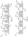
- FIG. 5 depicts a cross-sectional view of another (second) alternative embodiment of the inventive diagnostic wafer 401 having one or more independent ion energy analyzer and ion current probe combinations 300 imbedded within a "thick" placebo wafer 400.
- the ion energy analyzer and ion current probe combinations 300 are individually fabricated as described with reference to FIG. 4.
- the "thick" placebo wafer 400 contains a metal portion 402 having one or more apertures 404 and a ceramic (non-conductive) layer 406 deposited upon a surface 408 of the metallic portion 402. In use, the metallic portion abuts and is supported by a chuck (also known as a susceptor).
- a chuck also known as a susceptor
- an RF voltage is applied to the chuck as a biasing voltage.
- the metal portion of the placebo wafer extends the surface of the chuck.
- the metal portion is approximately 1.524 to 1.778 mm (60 to 70 mils) thick.
- the ceramic layer more or less imitates a semiconductor wafer resting upon the chuck.
- the ceramic layer is approximately 0.127 to 0.254 mm (5 to 10 mils) thick. In this manner, the probe combinations 300 do not protrude from the surface of the placebo wafer.
- the diagnostic wafer of this second alternative embodiment functions in the same manner as the first alternative embodiment described above.
- FIG. 6 depicts a partial cross sectional view of a micro-channel plate 600 that can be used in lieu of the floating grid described above.
- a composite diagnostic wafer having one or more ion energy analyzers with micro-channel plates forms a third embodiment of the invention.
- Such an ion energy analyzer having a micro-channel plate can be used in any of the foregoing embodiments of the invention.
- a micro-channel plate 600 provides depth to each passageway into the ion energy analyzer and, as such, provides ion trajectory discrimination, i.e., the thicker the plate, the more geometrically discriminating the analyzer and the narrower the angle over which incoming ions will be accepted into the analyzer.
- the plate 600 is typically fabricated of glass having a plurality of holes 602 (or micro-channels) formed in a honeycomb pattern through the plate.
- a micro-channel plate provides a trajectory discrimination scheme also known as a geometric filter.
- the plate thickness and micro-channel diameter define a critical angle 604 measured from the long axis 606 of a given micro-channel 602. Ions entering a micro-channel at a trajectory angle that is greater than the critical angle impact the walls of the micro-channel and do not enter the ion energy analyzer. On the other hand, ions with trajectory angles less than the critical angle pass into the analyzer for further discrimination (energy discrimination) by the discriminator grid.
- the holes had a diameter of 0.015 mm and a length of 0.6 mm which defined a critical angle of approximately 0.6 degrees. See R.L. Stenzel et al., "Novel Directional Ion Energy Analyzer", Rev. Sci. Instrum. 53(7), July 1982, pp. 1027-1031.
- the critical angle is a spherical angle.
- the micro-channels can be formed at an angle to the plane of the plate such that ions having certain trajectory angles plus or minus the critical angle are selected for measurement.
- FIG. 7 depicts a top plan view of a fourth alternative embodiment of the present invention.
- FIG. 8 depicts an exploded, cross-sectional view along line 8-8 shown in FIG. 7. To best understand this embodiment, FIGS. 7 and 8 should be viewed simultaneously.
- FIGS. 7 and 8 depict a composite diagnostic wafer containing an ion energy analyzer 104 and current probe 106 mounted upon a placebo wafer 102.
- the analyzer component parts are clamped together, rather than epoxied, to form a structurally sturdy analyzer device.
- a housing 700 of the analyzer 104 is attached to, or imbedded within, a placebo wafer 102.
- the housing 700 has a terraced inner surface and a substantially cylindrical outer surface.
- the housing is constructed of a solid anodized aluminum cylinder having the terraced inner surface milled therein. To provide electrical access to the grids, holes are drilled from the outer surface to the inner surface of the housing through which wires are threaded.
- the housing can be formed of a stack of anodized aluminum washers.
- a conductive trace and conductive through-hole can be formed on each washer prior to stacking. Once stacked, the washers can be welded, fused, or screwed to one another.
- the conductive traces and through holes provide an electrical path to the components of the analyzer.
- the collector disk 200 is positioned within the housing.
- the collector abuts conductive trace 704 such that current measuring instrumentation can be connected to the collector.
- Atop the collector and supported by the first terrace 702 is positioned annular insulator 202.
- Atop insulator 202 is positioned the secondary electron repelling grid 206.
- the grid 206 abuts a conductive trace 706 located on terrace 708 that supplies bias voltage to the grid.
- the second annular insulator 208 is positioned upon terrace 708.
- the discriminator grid 212 is positioned atop insulator 208 and abuts conductive trace 710 located on terrace 712.
- the third annular insulator 214 is positioned above grid 212 and is supported by terrace 712.
- the floating grid 218 is located on the top surface 718 of the housing 700 and abuts conductive trace 714.
- a clamping ring 716 is screwed, by screws 720, to the top surface 718 of the housing 700.
- the clamping ring maintains, by compressive force, the insulators and grids within the analyzer in a stationary position. Additionally, the compressive force maintains the grids in electrical contact with their respective conductive traces.
- a current probe 106 is attached, typically by a ceramic epoxy, to the top surface of the clamping ring 716. This ion energy analyzer and current probe combination operates in the exact same manner as the combinations described with respect to the other embodiments of the invention.
- the walls of the apertures in the "thick" placebo wafer of FIG. 5 can be terraced in the manner described above.
- an ion energy analyzer can be fabricated within each of the terraced apertures as described above.
- each of the foregoing embodiments of the invention are able to substantially simultaneously measure both ion current and ion energy. Furthermore, both measurements can be accomplished at generally the same physical location on the placebo wafer.
- a plurality of ion probe and ion energy analyzer combinations distributed over the surface of a placebo wafer two-dimensional ion current and ion energy maps can be generated to fully characterize a plasma over the surface of the placebo wafer.
Landscapes
- Physics & Mathematics (AREA)
- Engineering & Computer Science (AREA)
- Plasma & Fusion (AREA)
- Chemical & Material Sciences (AREA)
- Analytical Chemistry (AREA)
- Testing Or Measuring Of Semiconductors Or The Like (AREA)
- Holo Graphy (AREA)
- Lubrication Of Internal Combustion Engines (AREA)
- Sampling And Sample Adjustment (AREA)
- Plasma Technology (AREA)
- Drying Of Semiconductors (AREA)
- Testing Of Individual Semiconductor Devices (AREA)
Claims (31)
- Diagnostikwafer (100; 301; 401) mit:einem Placebowafer (102; 400);einer auf dem Placebowafer (102; 400) angebrachten Ionenstromsonde (106); undeinem auf dem Placebowafer (102; 400) angebrachten Ionenenergieanalysator (104).
- Diagnostikwafer gemäß Anspruch 1, der des weiteren eine Mehrzahl von auf dem Placebowafer (102; 400) angebrachten Ionenstromsonden (106) aufweist.
- Diagnostikwafer gemäß mindestens einem der vorhergehenden Ansprüche, der des weiteren eine Mehrzahl von auf dem Placebowafer (102; 400) angebrachten Ionenenergieanalysatoren (104) aufweist.
- Diagnostikwafer gemäß mindestens einem der vorhergehenden Ansprüche, bei dem der Placebowafer (102; 400) des weiteren mindestens eine Erweiterung (110) aufweist, welche sich von einem Umfang des Placebowafers (102; 400) erstreckt.
- Diagnostikwafer gemäß mindestens einem der vorhergehenden Ansprüche, bei dem die Ionenstromsonde (106) koaxial an dem Ionenenergieanalysator (104) angebracht ist, und der Ionenenergieanalysator (104) an dem Placebowafer (102; 400) angebracht ist.
- Diagnostikwafer gemäß mindestens einem der vorhergehenden Ansprüche, bei dem die Ionenstromsonde (106) und der Ionenenergieanalysator (104) im wesentlichen zusammen auf dem Placebowafer (102; 400) angeordnet sind.
- Diagnostikwafer gemäß mindestens einem der vorhergehenden Ansprüche, bei dem der Energieanalysator (104) des weiteren folgendes aufweist:eine an dem Placebowafer (102; 400) angebrachte Kollektorplatte (200);einen an der Kollektorplatte (200) angebrachten Diskriminatorgitterringisolator (208) mit einer zentralen Öffnung (210) in Ausrichtung mit einem Zentrum der Kollektorplatte (200);ein Diskriminatorgitter (212) an dem Diskriminatorgitterringisolator (208), welches die zentrale Öffnung (210) hiervon überspannt und von der Kollektorplatte (200) beabstandet ist;einen Floating-Gitter-Ringisolator (214), der an dem Diskriminatorgitter (212) angebracht ist, mit einer zentralen Öffnung (216) in Ausrichtung mit einem Zentrum der zentralen Öffnung (210) des Diskriminatorgitterringisolators (208); undein Floating-Gitter (218) an dem Floating-Gitter-Ringisolator (214), welches die zentrale Öffnung (216) hiervon überspannt und von dem Diskriminatorgitter (212) beabstandet ist.
- Diagnostikwafer gemäß mindestens einem der vorhergehenden Ansprüche, bei dem der Energieanalysator (104) des weiteren folgendes aufweist:einen Sekundärelektronenabstoßgitter-Ringisolator (202) zwischen der Kollektorplatte (200) und dem Diskriminatorgitterringisolator (208) mit einer zentralen Öffnung (204) in Ausrichtung mit einem Zentrum der zentralen Öffnung (210) des Diskriminatorgitterringisolators (208); undein Sekundärelektronenabstoßgitter (206) an dem Sekundärelektronenabstoßgitter-Ringisolator (202), welches die zentrale Öffnung (204) hiervon überspannt und von der Kollektorplatte (200) beabstandet ist.
- Diagnostikwafer gemäß mindestens einem der Ansprüche 7 bis 8 mit einer an dem Floating-Gitter (218) angebrachten Ionenstromsonde (106).
- Diagnostikwafer gemäß mindestens einem der Ansprüche 7 bis 9, bei dem das Floating-Gitter (218) eine Mikrokanalplatte (600) ist.
- Diagnostikwafer gemäß mindestens einem der vorhergehenden Ansprüche, bei dem der Energieanalysator (104) in einem Gehäuse (700) mit einer terrassenförmigen inneren Oberfläche gebildet ist, wo der Diskriminatorgitterringisolator (208) auf dem Kollektor (200) durch eine erste Terrasse (708) getragen ist, wobei das Diskriminatorgitter (212) und der Floating-Gitter-Ringisolator (214) durch eine zweite Terrasse (712) getragen sind, das Floating-Gitter (218) durch eine obere Oberfläche (718) des Gehäuses (700) getragen ist und ein Klemmring (716) an der oberen Oberfläche (718) des Gehäuses (700) angebracht ist, um den Kollektor (200), den Diskriminatorgitterringisolator (208), das Diskriminatorgitter (212), den Floating-Gitter-Ringisolator (214) und das Floating-Gitter (218) innerhalb des Gehäuses (700) festzuklemmen.
- Diagnostikwafer gemäß mindestens einem der Ansprüche 8 bis 10, bei dem der Energieanalysator (104) in einem Gehäuse (700) mit einer terrassenförmigen inneren Oberfläche gebildet ist, wo der Sekundärelektronenabstoßgitter-Ringisolator (202) auf dem Kollektor (200) durch eine erste Terrasse (702) getragen ist, wobei das Sekundärelektronenabstoßgitter (206) und der Diskriminatorgitterringisolator (208) durch eine zweite Terrasse (708) getragen sind, das Diskriminatorgitter (212) und der Floating-Gitter-Ringisolator (214) durch eine dritte Terrasse (712) getragen sind, das Floating-Gitter (218) durch eine obere Oberfläche (718) des Gehäuses (700) getragen ist, und ein Klemmring (716) an der oberen Oberfläche (718) des Gehäuses (700) angebracht ist, um den Kollektor (200), den Sekundärelektronenabstoßgitter-Ringisolator (202), das Sekundärelektronenabstoßgitter (206), den Diskriminatorgitterringisolator (208), das Diskriminatorgitter (212), den Floating-Gitter-Ringisolator (214) und das Floating-Gitter (218) innerhalb des Gehäuses (700) festzuklemmen.
- Diagnostikwafer gemäß mindestens einem der Ansprüche 7 bis 12, bei dem eine Mehrzahl von Leitspuren (704, 710, 714) durch das Gehäuse (700) mit dem Kollektor (200), dem Diskriminatorgitter (212) und dem Floating-Gitter (218) verbunden ist.
- Diagnostikwafer gemäß mindestens einem der Ansprüche 8 bis 12, bei dem eine Mehrzahl von Leitspuren (704, 706, 710, 714) durch das Gehäuse (700) mit dem Kollektor (200), dem Sekundärelektronenabstoßgitter (206), dem Diskriminatorgitter (212) und dem Floating-Gitter (218) verbunden ist.
- Diagnostikwafer gemäß mindestens einem der vorhergehenden Ansprüche, bei dem:der Placebowafer (102; 400) eine darin ausgebildete Öffnung (404) aufweist;wobei der Analysator (104) und die Sonde (106) im wesentlichen in Deckung mit der Öffnung sind.
- Diagnostikwafer gemäß Anspruch 15, bei dem der Ionenenergieanalysator (104) innerhalb der Öffnung (404) positioniert ist.
- Diagnostikwafer gemäß mindestens einem der Ansprüche 15 oder 16, bei dem die Ionenstromsonde (106) im wesentlichen zusammen mit dem Ionenenergieanalysator (104) angeordnet ist.
- Diagnostikwafer gemäß mindestens einem der Ansprüche 15 bis 17, bei dem die Ionenstromsonde (106) an dem Ionenenergieanalysator (104) angebracht ist.
- Diagnostikwafer gemäß mindestens einem der Ansprüche 15 bis 18, bei dem der Placebowafer (102; 400) des weiteren einen leitenden Bereich (402) und eine isolierende Schicht (406) aufweist, welche über einer Oberfläche des leitenden Bereichs (402) gebildet ist.
- Diagnostikwafer gemäß mindestens einem der Ansprüche 15 bis 19, bei dem der Placebowafer (102; 400) eine Mehrzahl von Öffnungen (404) aufweist und jede Öffnung (404) einen Ionenenergieanalysator (104) umfaßt.
- Diagnostikwafer gemäß mindestens einem der Ansprüche 15 bis 20, bei dem der Placebowafer (102; 400) eine Mehrzahl von Ionenstromsonden (106) trägt.
- Diagnostikwafer gemäß mindestens einem der Ansprüche 15 bis 21, bei dem die Ionenstromsonde (106) koaxial an dem Ionenenergieanalysator (104) angebracht ist und der Ionenenergieanalysator (104) innerhalb der Öffnung (404) angeordnet ist.
- Diagnostikwafer gemäß mindestens einem der Ansprüche 15 bis 22, bei dem der Placebowafer (102; 400) des weiteren mindestens eine Erweiterung (110) aufweist, welche sich von einem umfang des Placebowafers (102; 400) erstreckt.
- Diagnostikwafer gemäß mindestens einem der Ansprüche 15 bis 23, bei dem der Energieanalysator (104) des weiteren folgendes aufweist:eine innerhalb der Öffnung in dem Placebowafer (102; 400) angeordnete Kollektorplatte (200);einen an der Kollektorplatte (200) angebrachten Diskriminatorgitterringisolator (208) mit einer zentralen Öffnung (210) in Ausrichtung mit einem Zentrum der Kollektorplatte (200);ein Diskriminatorgitter (212) an dem Diskriminatorgitterringisolator (208), welches die zentrale Öffnung (210) hiervon überspannt und von der Kollektorplatte (200) beabstandet ist;einen Floating-Gitter-Ringisolator (214), der an dem Diskriminatorgitter (212) angebracht ist, mit einer zentralen Offnung (216) in Ausrichtung mit einem Zentrum der zentralen Öffnung (210) des Diskriminatorgitterringisolators (208); undein Floating-Gitter (218) an dem Floating-Gitter-Ringisolator (214), welches die zentrale Öffnung (216) hiervon überspannt und von dem Diskriminatorgitter (212) beabstandet ist.
- Diagnostikwafer gemäß mindestens einem der Ansprüche 15 bis 24, bei dem der Energieanalysator des weiteren folgendes aufweist:einen Sekundärelektronenabstoßgitter-Ringisolator (202) zwischen der Kollektorplatte (200) und dem Diskriminatorgitterringisolator (208) mit einer zentralen Öffnung (204) in Ausrichtung mit einem Zentrum der zentralen Öffnung (210) des Diskriminatorgitterringisolators (208); undein Sekundärelektronenabstoßgitter (206) an dem Sekundärelektronenabstoßgitter-Ringisolator (202), welches die zentrale Öffnung (204) hiervon überspannt und von der Kollektorplatte (200) beabstandet ist.
- Diagnostikwafer gemäß mindestens einem der Ansprüche 24 oder 25 mit einer an dem Floating-Gitter (218) angebrachten Ionenstromsonde (106).
- Diagnostikwafer gemäß mindestens einem der Ansprüche 24 bis 26, bei dem das Floating-Gitter (218) eine Mikrokanaiplatte (600) ist.
- Diagnostikwafer gemäß mindestens einem der Ansprüche 15 bis 27, bei dem die Öffnung (404) in dem Placebowafer (102; 400) eine terrassenförmige innere Oberfläche aufweist und der Energieanalysator (104) auf der terrassenförmigen inneren Oberfläche gebildet ist, wo der Diskriminatorgitterringisolator (208) auf dem Kollektor (200) durch eine erste Terrasse (708) getragen ist, wobei das Diskriminatorgitter (212) und der Floating-Gitter-Ringisolator (214) durch eine zweite Terrasse (712) getragen sind, das Floating-Gitter (218) durch eine obere Oberfläche (718) des Gehäuses (700) getragen ist und ein Klemmring (716) an der oberen Oberfläche (718) des Gehäuses (700) angebracht ist, um den Kollektor (200), den Diskriminatorgitterringisolator (208), das Diskriminatorgitter (212), den Floating-Gitter-Ringisolator (214) und das Floating-Gitter (218) innerhalb des Gehäuses (700) festzuklemmen.
- Diagnostikwafer gemäß mindestens einem der Ansprüche 25 bis 28, bei dem die Öffnung (404) in dem Placebowafer (102; 400) eine terrassenförmmige innere Oberfläche aufweist und der Energieanalysator (104) auf der terrassenförmigen inneren Oberfläche gebildet ist, wo der Sekundärelektronenabstoßgitter-Ringisolator (202) auf dem Kollektor (200) durch eine erste Terrasse (702) getragen ist, wobei das Sekundärelektronenabstoßgitter (206) und der Diskriminatorgitterringisolator (208) durch eine zweite Terrasse (708) getragen sind, das Diskriminatorgitter (212) und der Floating-Gitter-Ringisolator (214) durch eine dritte Terrasse (712) getragen sind, das Floating-Gitter (218) durch eine obere Oberfläche (718) des Gehäuses (700) getragen ist, und ein Klemmring (716) an der oberen Oberfläche (718) des Gehäuses (700) angebracht ist, um den Kollektor (200), den Sekundärelektronenabstoßgitter-Ringisolator (202), das Sekundärelektronenabstoßgitter (206), den Diskriminatorgitterringisolator (208), das Diskriminatorgitter (212), den Floating-Gitter-Ringisolator (214) und das Floating-Gitter (218) innerhalb des Gehäuses (700) festzuklemmen.
- Diagnostikwafer gemäß mindestens einem der Ansprüche 24 bis 29, bei dem eine Mehrzahl von Leitspuren (704, 710, 714) durch das Gehäuse (700) mit dem Kollektor (200), dem Diskriminatorgitter (212) und dem Floating-Gitter (218) verbunden ist.
- Diagnostikwafer gemäß mindestens einem der Ansprüche 24 bis 29, bei dem eine Mehrzahl von Leitspuren (704, 706, 710, 714) durch das Gehäuse (700) mit dem Kollektor (200), dem Sekundärelektronenabstoßgitter (206), dem Diskriminatorgitter (212) und dem Floating-Gitter (218) verbunden ist.
Applications Claiming Priority (2)
| Application Number | Priority Date | Filing Date | Title |
|---|---|---|---|
| US08/331,836 US5451784A (en) | 1994-10-31 | 1994-10-31 | Composite diagnostic wafer for semiconductor wafer processing systems |
| US331836 | 1994-10-31 |
Publications (2)
| Publication Number | Publication Date |
|---|---|
| EP0709874A1 EP0709874A1 (de) | 1996-05-01 |
| EP0709874B1 true EP0709874B1 (de) | 1998-08-26 |
Family
ID=23295570
Family Applications (1)
| Application Number | Title | Priority Date | Filing Date |
|---|---|---|---|
| EP95117154A Expired - Lifetime EP0709874B1 (de) | 1994-10-31 | 1995-10-31 | Diagnostische Scheibe |
Country Status (6)
| Country | Link |
|---|---|
| US (1) | US5451784A (de) |
| EP (1) | EP0709874B1 (de) |
| JP (1) | JPH08213374A (de) |
| KR (1) | KR100353957B1 (de) |
| AT (1) | ATE170330T1 (de) |
| DE (1) | DE69504275T2 (de) |
Families Citing this family (45)
| Publication number | Priority date | Publication date | Assignee | Title |
|---|---|---|---|---|
| US5451784A (en) * | 1994-10-31 | 1995-09-19 | Applied Materials, Inc. | Composite diagnostic wafer for semiconductor wafer processing systems |
| US5565681A (en) * | 1995-03-23 | 1996-10-15 | Applied Materials, Inc. | Ion energy analyzer with an electrically controlled geometric filter |
| US5801386A (en) * | 1995-12-11 | 1998-09-01 | Applied Materials, Inc. | Apparatus for measuring plasma characteristics within a semiconductor wafer processing system and a method of fabricating and using same |
| GB9620151D0 (en) * | 1996-09-27 | 1996-11-13 | Surface Tech Sys Ltd | Plasma processing apparatus |
| JP3006535B2 (ja) * | 1997-04-07 | 2000-02-07 | 日本電気株式会社 | イオン注入方法および装置 |
| US5989349A (en) * | 1997-06-24 | 1999-11-23 | Applied Materials, Inc. | Diagnostic pedestal assembly for a semiconductor wafer processing system |
| US6406785B1 (en) * | 1998-07-16 | 2002-06-18 | Schlegel Corporation | Weatherseal having a contact layer with thermoplastic particles in a thermoset carrier |
| KR100448529B1 (ko) * | 1999-03-17 | 2004-09-13 | 가부시키가이샤 히타치세이사쿠쇼 | 이온전류밀도 측정방법 및 측정장치 및 반도체디바이스제조방법 |
| JP4776783B2 (ja) * | 1999-05-07 | 2011-09-21 | 東京エレクトロン株式会社 | 基板処理方法及び基板処理装置 |
| US6409896B2 (en) | 1999-12-01 | 2002-06-25 | Applied Materials, Inc. | Method and apparatus for semiconductor wafer process monitoring |
| TW525213B (en) * | 2000-02-16 | 2003-03-21 | Hitachi Ltd | Process monitoring methods in a plasma processing apparatus, monitoring units, and a sample processing method using the monitoring units |
| US7091503B2 (en) | 2000-05-05 | 2006-08-15 | Tokyo Electron Limited | Measuring plasma uniformity in-situ at wafer level |
| US6741446B2 (en) | 2001-03-30 | 2004-05-25 | Lam Research Corporation | Vacuum plasma processor and method of operating same |
| US7960670B2 (en) * | 2005-05-03 | 2011-06-14 | Kla-Tencor Corporation | Methods of and apparatuses for measuring electrical parameters of a plasma process |
| US20030139043A1 (en) * | 2001-12-11 | 2003-07-24 | Steve Marcus | Apparatus and method for monitoring a plasma etch process |
| US6812725B2 (en) | 2002-02-27 | 2004-11-02 | Hitachi, Ltd. | Semiconductor processing apparatus and wafer sensor module |
| JP4175456B2 (ja) * | 2002-03-26 | 2008-11-05 | 株式会社 東北テクノアーチ | オンウエハ・モニタリング・システム |
| KR100450979B1 (ko) * | 2002-05-02 | 2004-10-02 | 강대환 | 플라즈마 진단용 웨이퍼 제조 방법 |
| US20050011611A1 (en) * | 2002-07-12 | 2005-01-20 | Mahoney Leonard J. | Wafer probe for measuring plasma and surface characteristics in plasma processing environments |
| US20040016402A1 (en) * | 2002-07-26 | 2004-01-29 | Walther Steven R. | Methods and apparatus for monitoring plasma parameters in plasma doping systems |
| DE10258118A1 (de) * | 2002-12-06 | 2004-07-08 | Fraunhofer-Gesellschaft zur Förderung der angewandten Forschung e.V. | Vorrichtung und Verfahren zum Messen und zur Bestimmung von Ladungsträgerströmen und davon ableitbaren Größen in ionen- und plasmagestützten Prozessen |
| US6902646B2 (en) * | 2003-08-14 | 2005-06-07 | Advanced Energy Industries, Inc. | Sensor array for measuring plasma characteristics in plasma processing environments |
| JP4008899B2 (ja) * | 2003-09-08 | 2007-11-14 | 株式会社東芝 | 半導体装置の製造システムおよび半導体装置の製造方法 |
| JP3868427B2 (ja) | 2004-02-23 | 2007-01-17 | 株式会社半導体理工学研究センター | プラズマプロセスのリアルタイムモニタ装置 |
| US7878145B2 (en) * | 2004-06-02 | 2011-02-01 | Varian Semiconductor Equipment Associates, Inc. | Monitoring plasma ion implantation systems for fault detection and process control |
| US20050284570A1 (en) * | 2004-06-24 | 2005-12-29 | Doran Daniel B | Diagnostic plasma measurement device having patterned sensors and features |
| US20060043063A1 (en) * | 2004-09-02 | 2006-03-02 | Mahoney Leonard J | Electrically floating diagnostic plasma probe with ion property sensors |
| US20060049036A1 (en) * | 2004-09-09 | 2006-03-09 | Taiwan Semiconductor Manufacturing Company, Ltd. | Method and apparatus for real-time control and monitor of deposition processes |
| US20060171848A1 (en) * | 2005-01-31 | 2006-08-03 | Advanced Energy Industries, Inc. | Diagnostic plasma sensors for endpoint and end-of-life detection |
| US20060266288A1 (en) * | 2005-05-27 | 2006-11-30 | Applied Materials, Inc. | High plasma utilization for remote plasma clean |
| KR100782370B1 (ko) | 2006-08-04 | 2007-12-07 | 삼성전자주식회사 | 지연 전기장을 이용한 이온 에너지 분포 분석기에 근거한이온 분석 시스템 |
| US7867409B2 (en) * | 2007-03-29 | 2011-01-11 | Tokyo Electron Limited | Control of ion angular distribution function at wafer surface |
| US7777179B2 (en) * | 2008-03-31 | 2010-08-17 | Tokyo Electron Limited | Two-grid ion energy analyzer and methods of manufacturing and operating |
| US7875859B2 (en) * | 2008-03-31 | 2011-01-25 | Tokyo Electron Limited | Ion energy analyzer and methods of manufacturing and operating |
| KR20120106712A (ko) | 2009-07-02 | 2012-09-26 | 이 아이 듀폰 디 네모아 앤드 캄파니 | 반도체 제조 부품 |
| US20110000617A1 (en) | 2009-07-02 | 2011-01-06 | E. I. Du Pont De Nemours And Company | Process for making a composite |
| US8847159B2 (en) | 2011-03-28 | 2014-09-30 | Tokyo Electron Limited | Ion energy analyzer |
| TW201705183A (zh) * | 2015-07-31 | 2017-02-01 | 逢甲大學 | 超高頻電漿模擬裝置與超高頻電漿特性量測方法 |
| JP2017188236A (ja) * | 2016-04-03 | 2017-10-12 | 国立大学法人東北大学 | プラズマ処理装置におけるプラズマ状態の計測方法及びその計測方法に使用されるプラズマ計測装置 |
| EP3968353A1 (de) * | 2020-09-10 | 2022-03-16 | Impedans Ltd | Vorrichtung zur ionenenergieanalyse von plasmaprozessen |
| US11264212B1 (en) | 2020-09-29 | 2022-03-01 | Tokyo Electron Limited | Ion angle detector |
| EP4177928B1 (de) | 2021-11-09 | 2024-01-03 | Impedans Ltd | Verfahren zur zweistufigen ionenstrommessung in einer vorrichtung zur analyse von plasmaprozessen |
| JPWO2024005004A1 (de) * | 2022-06-30 | 2024-01-04 | ||
| KR20250029901A (ko) * | 2022-06-30 | 2025-03-05 | 도쿄엘렉트론가부시키가이샤 | 플라즈마 처리 방법 및 플라즈마 처리 장치 |
| EP4625471A3 (de) * | 2022-11-25 | 2025-12-31 | Applied Materials, Inc. | Abgeschirmte vorrichtung zur ionenenergieanalyse von plasmaprozessen |
Family Cites Families (10)
| Publication number | Priority date | Publication date | Assignee | Title |
|---|---|---|---|---|
| GB1596105A (en) * | 1978-02-20 | 1981-08-19 | Nat Res Dev | Electrostatic engergy analysis |
| JPS56126918A (en) * | 1980-03-11 | 1981-10-05 | Hitachi Ltd | Injecting device for ion |
| US4680468A (en) * | 1985-08-05 | 1987-07-14 | Canadian Patents And Development Limited-Societe Canadienne Des Brevets Et D'exploitation Limitee | Particle detector |
| US4980562A (en) * | 1986-04-09 | 1990-12-25 | Varian Associates, Inc. | Method and apparatus for high efficiency scanning in an ion implanter |
| US4731538A (en) * | 1986-06-20 | 1988-03-15 | Galileo Electro-Optics Corp. | Microchannel plate ion detector |
| JPS63126148A (ja) * | 1986-11-14 | 1988-05-30 | Hiroshi Daimon | 荷電粒子アナライザ− |
| US4831267A (en) * | 1987-02-16 | 1989-05-16 | Siemens Aktiengesellschaft | Detector for charged particles |
| JPH0770296B2 (ja) * | 1989-05-15 | 1995-07-31 | 日新電機株式会社 | イオン注入装置 |
| GB2262649B (en) * | 1991-12-13 | 1995-03-01 | Marconi Gec Ltd | Energy analyser |
| US5451784A (en) * | 1994-10-31 | 1995-09-19 | Applied Materials, Inc. | Composite diagnostic wafer for semiconductor wafer processing systems |
-
1994
- 1994-10-31 US US08/331,836 patent/US5451784A/en not_active Expired - Lifetime
-
1995
- 1995-10-31 EP EP95117154A patent/EP0709874B1/de not_active Expired - Lifetime
- 1995-10-31 KR KR1019950038301A patent/KR100353957B1/ko not_active Expired - Fee Related
- 1995-10-31 DE DE69504275T patent/DE69504275T2/de not_active Expired - Fee Related
- 1995-10-31 AT AT95117154T patent/ATE170330T1/de not_active IP Right Cessation
- 1995-10-31 JP JP7283544A patent/JPH08213374A/ja not_active Withdrawn
Also Published As
| Publication number | Publication date |
|---|---|
| KR960015837A (ko) | 1996-05-22 |
| DE69504275T2 (de) | 1999-05-06 |
| JPH08213374A (ja) | 1996-08-20 |
| EP0709874A1 (de) | 1996-05-01 |
| US5451784A (en) | 1995-09-19 |
| DE69504275D1 (de) | 1998-10-01 |
| KR100353957B1 (ko) | 2002-12-26 |
| ATE170330T1 (de) | 1998-09-15 |
Similar Documents
| Publication | Publication Date | Title |
|---|---|---|
| EP0709874B1 (de) | Diagnostische Scheibe | |
| EP0734044B1 (de) | Ionenenergie Analysator und elektrisch gesteuerter geometrischer Filter für einen solchen Analysator | |
| KR101967490B1 (ko) | 이온 에너지 분석기, 그 내부에서의 전기 신호화 방법, 그 제작 방법 및 작동 방법 | |
| EP1884984B1 (de) | Ionenanalysesystem auf der Grundlage eines Analysemittels für Ionenenergieverteilung unter Benutzung eines retardierten elektrischen Feldes | |
| US6180942B1 (en) | Ion detector, detector array and instrument using same | |
| US4983833A (en) | Device for the detecting of charged secondary particles | |
| US4680467A (en) | Electron spectroscopy system for chemical analysis of electrically isolated specimens | |
| JP4972405B2 (ja) | 仮想イオントラップ | |
| US4131799A (en) | Ionization chamber | |
| KR101356847B1 (ko) | 이온 빔 각 측정 시스템 및, 이온 주입 시스템을 위한 가변각 슬롯 어레이를 사용하는 방법 | |
| Ingram et al. | Design and use of a gridded probe in a low‐pressure rf argon discharge | |
| Ackermans et al. | Simultaneous energy and angle resolved ion scattering spectroscopy | |
| US12555756B2 (en) | System and method to measure ion properties in a plasma system | |
| JPS5841623B2 (ja) | 質量分析装置のイオン検出器 | |
| CN119199947A (zh) | 离子束流均匀度测量装置 | |
| JPH04171837A (ja) | イオンビーム形状測定具 | |
| JPH0616404B2 (ja) | 加速器結合透過型電子顕微鏡 | |
| Amsterdam | Microstrip Gas Counters in the lab and in the real world | |
| Civinini | The CMS silicon strip sensors | |
| Udo | Microstrip gas counters in the lab and in the real world | |
| JPH04133441U (ja) | ウエーハの帯電状態計測装置 | |
| JPH0458142B2 (de) | ||
| WO2010094605A1 (en) | Ion mass determination |
Legal Events
| Date | Code | Title | Description |
|---|---|---|---|
| PUAI | Public reference made under article 153(3) epc to a published international application that has entered the european phase |
Free format text: ORIGINAL CODE: 0009012 |
|
| AK | Designated contracting states |
Kind code of ref document: A1 Designated state(s): AT BE CH DE ES FR GB GR IE IT LI NL SE |
|
| 17P | Request for examination filed |
Effective date: 19961028 |
|
| GRAG | Despatch of communication of intention to grant |
Free format text: ORIGINAL CODE: EPIDOS AGRA |
|
| 17Q | First examination report despatched |
Effective date: 19971013 |
|
| GRAG | Despatch of communication of intention to grant |
Free format text: ORIGINAL CODE: EPIDOS AGRA |
|
| GRAG | Despatch of communication of intention to grant |
Free format text: ORIGINAL CODE: EPIDOS AGRA |
|
| GRAH | Despatch of communication of intention to grant a patent |
Free format text: ORIGINAL CODE: EPIDOS IGRA |
|
| GRAH | Despatch of communication of intention to grant a patent |
Free format text: ORIGINAL CODE: EPIDOS IGRA |
|
| GRAA | (expected) grant |
Free format text: ORIGINAL CODE: 0009210 |
|
| AK | Designated contracting states |
Kind code of ref document: B1 Designated state(s): AT BE CH DE ES FR GB GR IE IT LI NL SE |
|
| PG25 | Lapsed in a contracting state [announced via postgrant information from national office to epo] |
Ref country code: LI Free format text: LAPSE BECAUSE OF FAILURE TO SUBMIT A TRANSLATION OF THE DESCRIPTION OR TO PAY THE FEE WITHIN THE PRESCRIBED TIME-LIMIT Effective date: 19980826 Ref country code: IT Free format text: LAPSE BECAUSE OF FAILURE TO SUBMIT A TRANSLATION OF THE DESCRIPTION OR TO PAY THE FEE WITHIN THE PRE;WARNING: LAPSES OF ITALIAN PATENTS WITH EFFECTIVE DATE BEFORE 2007 MAY HAVE OCCURRED AT ANY TIME BEFORE 2007. THE CORRECT EFFECTIVE DATE MAY BE DIFFERENT FROM THE ONE RECORDED.SCRIBED TIME-LIMIT Effective date: 19980826 Ref country code: GR Free format text: LAPSE BECAUSE OF FAILURE TO SUBMIT A TRANSLATION OF THE DESCRIPTION OR TO PAY THE FEE WITHIN THE PRESCRIBED TIME-LIMIT Effective date: 19980826 Ref country code: ES Free format text: THE PATENT HAS BEEN ANNULLED BY A DECISION OF A NATIONAL AUTHORITY Effective date: 19980826 Ref country code: CH Free format text: LAPSE BECAUSE OF FAILURE TO SUBMIT A TRANSLATION OF THE DESCRIPTION OR TO PAY THE FEE WITHIN THE PRESCRIBED TIME-LIMIT Effective date: 19980826 Ref country code: BE Free format text: LAPSE BECAUSE OF FAILURE TO SUBMIT A TRANSLATION OF THE DESCRIPTION OR TO PAY THE FEE WITHIN THE PRESCRIBED TIME-LIMIT Effective date: 19980826 Ref country code: AT Free format text: LAPSE BECAUSE OF FAILURE TO SUBMIT A TRANSLATION OF THE DESCRIPTION OR TO PAY THE FEE WITHIN THE PRESCRIBED TIME-LIMIT Effective date: 19980826 |
|
| REF | Corresponds to: |
Ref document number: 170330 Country of ref document: AT Date of ref document: 19980915 Kind code of ref document: T |
|
| REG | Reference to a national code |
Ref country code: CH Ref legal event code: EP |
|
| REF | Corresponds to: |
Ref document number: 69504275 Country of ref document: DE Date of ref document: 19981001 |
|
| ET | Fr: translation filed | ||
| REG | Reference to a national code |
Ref country code: IE Ref legal event code: FG4D |
|
| PG25 | Lapsed in a contracting state [announced via postgrant information from national office to epo] |
Ref country code: SE Free format text: LAPSE BECAUSE OF FAILURE TO SUBMIT A TRANSLATION OF THE DESCRIPTION OR TO PAY THE FEE WITHIN THE PRESCRIBED TIME-LIMIT Effective date: 19981126 |
|
| REG | Reference to a national code |
Ref country code: CH Ref legal event code: PL |
|
| PLBE | No opposition filed within time limit |
Free format text: ORIGINAL CODE: 0009261 |
|
| STAA | Information on the status of an ep patent application or granted ep patent |
Free format text: STATUS: NO OPPOSITION FILED WITHIN TIME LIMIT |
|
| 26N | No opposition filed | ||
| PG25 | Lapsed in a contracting state [announced via postgrant information from national office to epo] |
Ref country code: NL Free format text: LAPSE BECAUSE OF NON-PAYMENT OF DUE FEES Effective date: 20000501 |
|
| NLV4 | Nl: lapsed or anulled due to non-payment of the annual fee |
Effective date: 20000501 |
|
| REG | Reference to a national code |
Ref country code: GB Ref legal event code: IF02 |
|
| PGFP | Annual fee paid to national office [announced via postgrant information from national office to epo] |
Ref country code: FR Payment date: 20021008 Year of fee payment: 8 |
|
| PGFP | Annual fee paid to national office [announced via postgrant information from national office to epo] |
Ref country code: DE Payment date: 20021029 Year of fee payment: 8 |
|
| PGFP | Annual fee paid to national office [announced via postgrant information from national office to epo] |
Ref country code: GB Payment date: 20021030 Year of fee payment: 8 |
|
| PGFP | Annual fee paid to national office [announced via postgrant information from national office to epo] |
Ref country code: IE Payment date: 20031014 Year of fee payment: 9 |
|
| PG25 | Lapsed in a contracting state [announced via postgrant information from national office to epo] |
Ref country code: GB Free format text: LAPSE BECAUSE OF NON-PAYMENT OF DUE FEES Effective date: 20031031 |
|
| PG25 | Lapsed in a contracting state [announced via postgrant information from national office to epo] |
Ref country code: DE Free format text: LAPSE BECAUSE OF NON-PAYMENT OF DUE FEES Effective date: 20040501 |
|
| GBPC | Gb: european patent ceased through non-payment of renewal fee |
Effective date: 20031031 |
|
| PG25 | Lapsed in a contracting state [announced via postgrant information from national office to epo] |
Ref country code: FR Free format text: LAPSE BECAUSE OF NON-PAYMENT OF DUE FEES Effective date: 20040630 |
|
| REG | Reference to a national code |
Ref country code: FR Ref legal event code: ST |
|
| PG25 | Lapsed in a contracting state [announced via postgrant information from national office to epo] |
Ref country code: IE Free format text: LAPSE BECAUSE OF NON-PAYMENT OF DUE FEES Effective date: 20041101 |
|
| REG | Reference to a national code |
Ref country code: IE Ref legal event code: MM4A |