EP0709879A1 - Halbleiterherstellungsverfahren - Google Patents
Halbleiterherstellungsverfahren Download PDFInfo
- Publication number
- EP0709879A1 EP0709879A1 EP94921097A EP94921097A EP0709879A1 EP 0709879 A1 EP0709879 A1 EP 0709879A1 EP 94921097 A EP94921097 A EP 94921097A EP 94921097 A EP94921097 A EP 94921097A EP 0709879 A1 EP0709879 A1 EP 0709879A1
- Authority
- EP
- European Patent Office
- Prior art keywords
- oxidized film
- film
- gas
- oxidized
- wafer
- Prior art date
- Legal status (The legal status is an assumption and is not a legal conclusion. Google has not performed a legal analysis and makes no representation as to the accuracy of the status listed.)
- Withdrawn
Links
Images


Classifications
-
- H—ELECTRICITY
- H10—SEMICONDUCTOR DEVICES; ELECTRIC SOLID-STATE DEVICES NOT OTHERWISE PROVIDED FOR
- H10P—GENERIC PROCESSES OR APPARATUS FOR THE MANUFACTURE OR TREATMENT OF DEVICES COVERED BY CLASS H10
- H10P14/00—Formation of materials, e.g. in the shape of layers or pillars
- H10P14/60—Formation of materials, e.g. in the shape of layers or pillars of insulating materials
- H10P14/63—Formation of materials, e.g. in the shape of layers or pillars of insulating materials characterised by the formation processes
- H10P14/6302—Non-deposition formation processes
- H10P14/6304—Formation by oxidation, e.g. oxidation of the substrate
- H10P14/6306—Formation by oxidation, e.g. oxidation of the substrate of the semiconductor materials
- H10P14/6308—Formation by oxidation, e.g. oxidation of the substrate of the semiconductor materials of Group IV semiconductors
- H10P14/6309—Formation by oxidation, e.g. oxidation of the substrate of the semiconductor materials of Group IV semiconductors of silicon in uncombined form, i.e. pure silicon
-
- H—ELECTRICITY
- H10—SEMICONDUCTOR DEVICES; ELECTRIC SOLID-STATE DEVICES NOT OTHERWISE PROVIDED FOR
- H10P—GENERIC PROCESSES OR APPARATUS FOR THE MANUFACTURE OR TREATMENT OF DEVICES COVERED BY CLASS H10
- H10P14/00—Formation of materials, e.g. in the shape of layers or pillars
- H10P14/60—Formation of materials, e.g. in the shape of layers or pillars of insulating materials
- H10P14/63—Formation of materials, e.g. in the shape of layers or pillars of insulating materials characterised by the formation processes
- H10P14/6302—Non-deposition formation processes
- H10P14/6319—Formation by plasma treatments, e.g. plasma oxidation of the substrate
Definitions
- the present invention relates to a method for manufacturing semiconductors, and more particularly to a method of manufacturing semiconductors suited to an oxidizing process in a semiconductor manufacturing process.
- Oxidizing method widely used in an LSI manufacturing process are divided to a dry oxidizing method under atmospheric pressure and a wet oxidizing method.
- oxidization is executed by introducing an oxygen gas under a high pressure in a range from 900 °C to 1000 °C, so that such problems as distortion of a wafer due to heat or rediffussion of impurities occur.
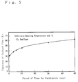
- Fig.5 shows a relation between a film thickness of a silicon oxidized film generated by oxygen plasma and a period of time required for oxidation.
- a pressure of the oxygen gas in this case is 6 mTorr, and an oxygen plasma is generated by loading a 50 W high frequency wave electric field having a frequency of 100 MHz thereto.
- a quantity of silicon oxidized film increase as time for oxidization becomes longer, which indicates that a surface of a silicon wafer is oxidized in an oxygen plasma.
- Fig.6 shows an X ray electron spectrographic spectrum of a silicon oxidized film (47 ⁇ ) formed by oxidizing a silicon wafer in an oxygen plasma.
- An X ray source used herein is AlK ⁇ . This figure shows 3 peaks caused due to existence of Si 2p . Namely, in addition to the peak 2b from the silicon wafer and peak 2a caused to existence of SiO2, the peak 2c can be observed.
- This peak 2c shows that bonding between Si and O other than SiO2 exists in an interface between Si and the silicon oxidized film or in the silicon oxidized film. If bonding between Si and O Other than SiO2 exists in an interface between Si and a silicon oxidized film or in the silicon oxidized film, dielectric strength fault easily occur in the oxidized film.
- Fig.7 shows a result of examination of a dielectric strength distribution in a MOS diode prepared by forming an oxidized film by way of oxidizing a silicon wafer in an oxygen plasma and than forming an Al electrode on the oxidized film.
- the dielectric strength is 10 MV/cm or more, but in a case of an oxidized film formed in an O2 film, the dielectric strength is at maximum 6 MV/cm, which is an extremely low value.
- oxidization in an oxygen plasma as employed in the conventional technology has a merit that an oxidized film can be obtained under a low pressure, but it has also a demerit that the insulating capability of the obtained oxidized film is substantially inferior to that of a thermally oxidized film.
- the method for manufacturing semiconductor according to the present invention is characterized in that, in a process for forming an oxidized film by oxidizing a surface of semiconductor wafer or of a metallic thin film, an oxidized film is formed in plasma atmosphere of a mixed gas including an inert and an oxygen gas for the inert gas to be included in the oxidized film.
- Fig.1 is a schematic diagram showing a key section of an oxidized film forming apparatus according to the present invention.
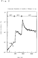
- Fig.2 is a graph showing dependence of a quantity of Ar gas released from an oxidized film formed according to the present invention on temperature.
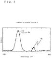
- Fig.3 shows an X ray photo-electron spectrum showing a bonding state between Si and O in an oxidized film formed according to the present invention.
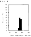
- Fig.4 is a histogram showing dielectric strength of an oxidized film formed according to the present invention.
- Fig.5 is a graph showing a relation between a thickness of an oxidized film formed according the conventional technology and a period of time required for oxidation.
- Fig.6 shows an X ray photo-electron spectrum showing a bonding state between Si and o in an oxidized film formed according to the conventional technology.
- Fig.7 is a histogram showing dielectric strength of an oxidized film formed according to the conventional technology.
- Fig.1 is a concept view showing an apparatus for oxidizing a semiconductor wafer with a plasma.
- the present apparatus is characterized in that a high frequency electric field having a frequency of, for instance, 100 MHz is loaded from a high frequency power source 101 to an upper electrode 103 to efficiently make an O2 gas and a Ar gas into a chamber discharge for the purpose to generate a plasma.
- an electric potential on a surface of a semiconductor wafer 106 place on the lower electrode 105 can be controlled.
- This electric potential can freely be changed by changing an output from the high frequency wave power source 104, and by providing controls so that the electric potential is smaller than that of an Ar/O2 mixed plasma, it is possible to irradiate Ar ions in an Ar plasma onto the semiconductor wafer surface 106. Also the semiconductor wafer 106 is heated by a heater 107.
- a difference between a plasma potential of the Ar/O2 mixed gas and a potential on the surface of the Si wafer 106 is 16 V, and it becomes possible to fully irradiate Ar+ ions onto the surface of the Si wafer.
- Ar ions By irradiating Ar ions it becomes possible to include Ar in a Si oxidized film when the Si wafer is oxidized.
- a quantity of Ar in the silicon oxide film manufactured as described above was measured. Change in a quantity of Ar atoms released from the oxidized film, when a silicon wafer is heated, in association with change in temperature is shown in Fig.2. A quantity of released Ar was measured according to the atmospheric pressure ionization mass spectrometry. As clearly shown in this film, in association with rise of temperature, a quantity of Ar released from the silicon oxidized film also increases, and it was found out the quantity of released Ar gas that 1 x 10¹⁴ to 5 x 10¹⁴ Ar atoms are included in the oxidized film.
- Fig.3 shows a result of investigation of a bonding state between Si atoms and O atoms in a silicon oxidized film according to the X ray photo-electron spectrography.
- a thickness of the oxidized film is 60 ⁇ .
- a source of x ray was an AlK ⁇ .
- a shown in this figure only the peal 6b from the silicon wafer and peak 6a from SiO2 as an oxidized film are observed, and it is determined that bonding between Si and O other than SiO2 does not exist therein.
- Fig.4 shows distribution of dielectric strength of a MOS diode manufactured by forming an Al electrode on an oxidized film having thickness of 60 ⁇ or more.
- the dielectric strength is at max 9 MV/cm, and when compared to that conventional type of oxidized film formed only with an O2 plasma shown in Fig.7, it is understood that the dielectric strength was improved by 3 MV/cm. Also the same measurement was executed to a MOS diode manufactured using an oxidized film from which an Ar gas was released, and the result shown in Fig.4 was obtained.
- a silicon oxidized film having high dielectric strength can be formed.
- description of the present embodiment above assumes oxidization of a silicon wafer, a semiconductor wafer is not limited to a silicon wafer, and this method is advantageously applied to oxidization of other types of semiconductor wafer or a metallic thin film formed on a semiconductor wafer. It has been confirmed that also a metallic thin film obtained by oxidizing a surface of metal (Ta) according to the sequence in this embodiment has higher dielectric strength.
- a thickness of the oxidized film was 60 ⁇ , but the thickness is not always limited to this value.
- a gas included in an oxidized film was an Ar gas, but other inert gas may be used for the purpose.
- the quantity of inert gas included in an oxidized gas in terms of a number of atoms was in a range from 1 x 10¹⁴ to 5 x 10¹⁴, but it is needless to say that the quantity is mot limited to this value.
- temperature of the silicon wafer 106 in the above description was 450 °C, the temperature is not limited to this value.
- atoms in a surface layer of a semiconductor wafer and oxygen atoms can be bonded to each other under stable conditions by having an inert gas included in the oxidized film, it is possible to provide a high quality semiconductor element having an oxidized film with high dielectric strength.
- an inert gas can effectively be included in an oxidized film in process of forming oxidized film.
Landscapes
- Formation Of Insulating Films (AREA)
- Crystals, And After-Treatments Of Crystals (AREA)
- Physical Vapour Deposition (AREA)
Applications Claiming Priority (3)
| Application Number | Priority Date | Filing Date | Title |
|---|---|---|---|
| JP5175738A JPH0729898A (ja) | 1993-07-15 | 1993-07-15 | 半導体製造方法 |
| JP175738/93 | 1993-07-15 | ||
| PCT/JP1994/001160 WO1995002896A1 (en) | 1993-07-15 | 1994-07-15 | Method for manufacturing semiconductor |
Publications (2)
| Publication Number | Publication Date |
|---|---|
| EP0709879A1 true EP0709879A1 (de) | 1996-05-01 |
| EP0709879A4 EP0709879A4 (de) | 1997-07-30 |
Family
ID=16001390
Family Applications (1)
| Application Number | Title | Priority Date | Filing Date |
|---|---|---|---|
| EP94921097A Withdrawn EP0709879A4 (de) | 1993-07-15 | 1994-07-15 | Halbleiterherstellungsverfahren |
Country Status (3)
| Country | Link |
|---|---|
| EP (1) | EP0709879A4 (de) |
| JP (1) | JPH0729898A (de) |
| WO (1) | WO1995002896A1 (de) |
Cited By (1)
| Publication number | Priority date | Publication date | Assignee | Title |
|---|---|---|---|---|
| US6746726B2 (en) | 1998-03-27 | 2004-06-08 | Tokyo University Of Agriculture & Technology | Method for forming film |
Families Citing this family (7)
| Publication number | Priority date | Publication date | Assignee | Title |
|---|---|---|---|---|
| JP4856297B2 (ja) * | 1997-12-02 | 2012-01-18 | 公益財団法人国際科学振興財団 | 半導体装置の製造方法 |
| JP3349968B2 (ja) | 1998-11-20 | 2002-11-25 | 日本電気株式会社 | 機器ユニット着脱構造 |
| TW533534B (en) * | 2002-02-01 | 2003-05-21 | Macronix Int Co Ltd | Manufacturing method of interpoly dielectric layer |
| JP4694771B2 (ja) * | 2003-03-12 | 2011-06-08 | 財団法人国際科学振興財団 | ポンプおよびポンプ部材の製造方法 |
| JP2006286662A (ja) * | 2005-03-31 | 2006-10-19 | Toshiba Corp | シリコン系被処理物の酸化処理方法、酸化処理装置および半導体装置の製造方法 |
| JP5357487B2 (ja) * | 2008-09-30 | 2013-12-04 | 東京エレクトロン株式会社 | シリコン酸化膜の形成方法、コンピュータ読み取り可能な記憶媒体およびプラズマ酸化処理装置 |
| JP4783845B2 (ja) | 2009-07-23 | 2011-09-28 | 東芝テック株式会社 | 電子機器 |
Family Cites Families (5)
| Publication number | Priority date | Publication date | Assignee | Title |
|---|---|---|---|---|
| JPS5825267A (ja) * | 1981-08-07 | 1983-02-15 | Matsushita Electric Ind Co Ltd | Mos型半導体装置およびその製造方法 |
| JPS6227533A (ja) * | 1985-07-26 | 1987-02-05 | Japan Synthetic Rubber Co Ltd | 内部酸化型合金およびその成形物の製造方法 |
| JPS62274627A (ja) * | 1986-05-23 | 1987-11-28 | Hitachi Ltd | 薄膜の製造方法 |
| JPH0273635A (ja) * | 1988-09-08 | 1990-03-13 | Nec Corp | 絶縁膜成長装置 |
| JPH06103691B2 (ja) * | 1989-02-20 | 1994-12-14 | 松下電器産業株式会社 | 薄膜の形成方法 |
-
1993
- 1993-07-15 JP JP5175738A patent/JPH0729898A/ja active Pending
-
1994
- 1994-07-15 EP EP94921097A patent/EP0709879A4/de not_active Withdrawn
- 1994-07-15 WO PCT/JP1994/001160 patent/WO1995002896A1/ja not_active Ceased
Cited By (1)
| Publication number | Priority date | Publication date | Assignee | Title |
|---|---|---|---|---|
| US6746726B2 (en) | 1998-03-27 | 2004-06-08 | Tokyo University Of Agriculture & Technology | Method for forming film |
Also Published As
| Publication number | Publication date |
|---|---|
| WO1995002896A1 (en) | 1995-01-26 |
| EP0709879A4 (de) | 1997-07-30 |
| JPH0729898A (ja) | 1995-01-31 |
Similar Documents
| Publication | Publication Date | Title |
|---|---|---|
| JP2687966B2 (ja) | 半導体装置の製造方法 | |
| US7217659B2 (en) | Process for producing materials for electronic device | |
| US6470824B2 (en) | Semiconductor manufacturing apparatus | |
| US3600218A (en) | Method for depositing insulating films of silicon nitride and aluminum nitride | |
| CN101944482B (zh) | 形成介电膜的方法 | |
| JPH09116104A (ja) | 半導体素子のキャパシタ製造方法 | |
| JP2009177161A (ja) | 絶縁膜の形成方法 | |
| KR20170042315A (ko) | 기판 처리 방법 | |
| EP0170848B1 (de) | Thermisches Ausglühen integrierter Schaltungen | |
| EP0709879A1 (de) | Halbleiterherstellungsverfahren | |
| US4645683A (en) | Method of manufacturing a semiconductor device | |
| US3419761A (en) | Method for depositing silicon nitride insulating films and electric devices incorporating such films | |
| TWI390675B (zh) | A gate insulating film forming method, a semiconductor device, and a computer recording medium | |
| CN1926670B (zh) | 等离子体处理方法 | |
| WO2006106667A1 (ja) | 絶縁膜の製造方法および半導体装置の製造方法 | |
| WO2007088904A1 (ja) | マイクロ波プラズマ処理装置 | |
| Valco et al. | Plasma deposited silicon nitride for gallium arsenide encapsulation | |
| CN101471256A (zh) | 形成介电膜的方法 | |
| US5938495A (en) | Method of manufacturing a field emission cold cathode capable of stably producing a high emission current | |
| Choi et al. | Electrical characterization of rapid thermal annealed radio frequency sputtered silicon oxide films | |
| US5418017A (en) | Method of forming oxide film | |
| JP4443819B2 (ja) | プラズマドーピング方法 | |
| Nagao et al. | Damageless vacuum sealing of Si field emitters with CHF 3 plasma treatment | |
| Valco et al. | Role of GaAs surface cleaning in plasma deposition of silicon nitride films for encapsulated annealing | |
| JP4356973B2 (ja) | ウェーハの金属汚染評価方法 |
Legal Events
| Date | Code | Title | Description |
|---|---|---|---|
| PUAI | Public reference made under article 153(3) epc to a published international application that has entered the european phase |
Free format text: ORIGINAL CODE: 0009012 |
|
| 17P | Request for examination filed |
Effective date: 19960214 |
|
| AK | Designated contracting states |
Kind code of ref document: A1 Designated state(s): CH DE FR GB IT LI NL |
|
| STAA | Information on the status of an ep patent application or granted ep patent |
Free format text: STATUS: THE APPLICATION HAS BEEN WITHDRAWN |
|
| A4 | Supplementary search report drawn up and despatched | ||
| AK | Designated contracting states |
Kind code of ref document: A4 Designated state(s): CH DE FR GB IT LI NL |
|
| 18W | Application withdrawn |
Withdrawal date: 19970628 |