EP0709882A2 - Halbleiterbauelement mit Passivierungsschicht aus einem Benzocycobuten-Polymer und Siliziumpulver - Google Patents
Halbleiterbauelement mit Passivierungsschicht aus einem Benzocycobuten-Polymer und Siliziumpulver Download PDFInfo
- Publication number
- EP0709882A2 EP0709882A2 EP95116915A EP95116915A EP0709882A2 EP 0709882 A2 EP0709882 A2 EP 0709882A2 EP 95116915 A EP95116915 A EP 95116915A EP 95116915 A EP95116915 A EP 95116915A EP 0709882 A2 EP0709882 A2 EP 0709882A2
- Authority
- EP
- European Patent Office
- Prior art keywords
- passivation layer
- silicon powder
- layer
- semiconductor device
- benzocyclobutene polymer
- Prior art date
- Legal status (The legal status is an assumption and is not a legal conclusion. Google has not performed a legal analysis and makes no representation as to the accuracy of the status listed.)
- Granted
Links
Images

Classifications
-
- H—ELECTRICITY
- H10—SEMICONDUCTOR DEVICES; ELECTRIC SOLID-STATE DEVICES NOT OTHERWISE PROVIDED FOR
- H10W—GENERIC PACKAGES, INTERCONNECTIONS, CONNECTORS OR OTHER CONSTRUCTIONAL DETAILS OF DEVICES COVERED BY CLASS H10
- H10W74/00—Encapsulations, e.g. protective coatings
- H10W74/40—Encapsulations, e.g. protective coatings characterised by their materials
- H10W74/47—Encapsulations, e.g. protective coatings characterised by their materials comprising organic materials, e.g. plastics or resins
Definitions
- the present invention relates to a semiconductor device and, more particularly, to an improved passivation layer thereof.
- impurity diffusion regions are formed in a semiconductor substrate, and metal layers are formed thereon to connect the impurity diffusion regions to each other.
- a surface of the device is protected by a dielectric cover which is called a passivation layer. That is, the passivation layer protects the device against external mechanical stress and prevents the device from being contaminated by external moisture and ions.
- a first prior art passivation layer is made of polyimide resin (see: JP-A-2-30171). This will be explained later in detail.
- the passivation layer cannot absorb roughness of a stepwise surface caused by multiple metal layers, so that flatness characteristics of the surface of the passivation layer cannot be obtained. Therefore, at a subsequent stage after the formation of the passivation layer, cracks and pinholes may be craeated in the passivation layer by thermal stress, mechanical stress and environmental stress applied to the rough stepwise surface, and the metal layers may be eroded by water and ions absorbed in the passivation layer due to its poor moistureproofness.
- a second prior art passivation layer includes a double layer configuration formed by a polyimide resin layer and a silicon nitride layer thereon (see JP-A-62-293726). This will also be explained later in detail.
- the silicon nitride layer has good moistureproofness, contact characteristics between the silicon nitride layer and the polyimide layer are deteriorated, so that water and ions are absorbed from the interface between the silicon nitride layer and the polyimide layer into the metal layers and the impurity diffusion regions of the device, thus reducing the reliability.
- a passivation layer is made of benzocyclobutene polymer and silicon powder.
- the benzocyclobutene polymer per se is flexible, so that the benzocyclobutene polymer can absorb stress applied thereto.
- the benzocyclobutene polymer has low water absorption properties, so as to exhibit good moistureproofness characteristics.
- the addition of silicon powder to the benzocyclobutene polymer makes the thermal expansivity of the passivation layer substantially equal that of a semiconducotor substrate such as a silicon substrate.
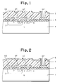
- Fig. 1 which illustrates a first prior art semiconductor device (see JP-A-2-30171)
- reference numeral 1 designates an N-type monocrystalline silicon substrate serving as a collector region
- 2 designates a P-type impurity diffusion region serving as a base region
- 3 designates an N+-type impurity diffusion region serving as an emitter region
- 4 designates an N+-type impurity diffusion region serving as a collector take-out region.
- Formed on the silicon substrate 1 is a silicon oxide layer having contact holes formed therein.
- a base electrode 6B, an emitter electrode 6E and a collector electrode 6C are formed on the silicon oxide layer 5 and are connected to the base region 2, the emitterregion 3 and the collector take-out region 4, respectively.
- an input/output pad 6P is formed on the silicon oxide layer 5.
- a polyimide resin layer 7 serving as a passivation layer.
- the polyimide resin layer 7 cannot absorb a roughness of a stepwise surface of the metal layers. That is, polyimide resin is formed by dehydrating polycondensation of a polyimide precursor, and therefore, in the dehydrating polycondesation process, the passivation layer is reduced in volume. As a result, the flatness characteristics of the polyimide resin layer 7 are deteriorated. Therefore, at a subsequent stage of the polyimide resin layer 7, cracks and pinholes may be created in the polyimide resin layer 7 by thermal stress, mechanical stress and environmental stress applied to the rough stepwise surface thereof. Also, the electrodes 6B, 6E, 6C and the pad 6P may be eroded by water and ions absorbed in the polyimide resin layer 7.
- a silicon nitride layer 8 is added to the elements of the device of Fig. 1, and accordingly, the silicon nitride layer 8 as well as the polyimide resin layer 7 serves as a passivation layer.
- the silicon nitride layer 8 has good moistureproofness, contact characteristics between the silicon nitride layer 8 and the polyimide layer 8 are deteriorated, so that water and ions are absorbed from the interface between the silicon nitride layer 8 and the polyimide layer 8 into the electrodes 6B, 6E, 6C, the pad 6P, and the impurity diffusion regions 2, 3 and 4. Thus, the reliability of the device is deteriorated.
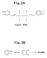
- Benzocylobutene polymer is formed by using benzocyclobutene monomer having a structural formula as shown in Fig. 3A. That is, the benzocylobutene monomer is heated, so that cyclobutene portions of the benzocylobutene monomer are ring-opened by a ring-open polymerization process as shown in Fig. 3B. In such a ring-open polymerization process, benzocyclobutene is never reduced in volume, which can absorb roughness of a stepwise surface of underlying layers.
- silicon powder whose particle diameter is about 1 ⁇ m, for example, is loaded to the benzocylobutene polymer as a passivation layer, so as to make the thermal expansibity of the passivation layer substantially equal that of a silicon substrate.
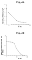
- the weight ratio of silicon powder to benzocyclobutene polymer is preferbly larger than approximately 1%. That is, as shown in Fig. 4A, which shows residual stress characteristics of a mixture of benzocylobutene and silicon powder, when the weight ratio of silicon powder is smaller than approximately 1%, the residual stress is remarkably increased, thus reducing the reliability of the passivation layer, particularly, in a large scale chip.
- the weight ratio of silicon powder to benzocyclobutene polymer is preferably smaller than approximately 90%. That is, as shown in Fig. 4B, which shows tensile elongation characteristics at break of a mixture of benzocyclobutene polymer and silicon powder, when the weight ratio of silicon powder is larger than approximately 90%, the tensile elongation rate at break is substantially 0%, so that cracks and pinholes are easily created in the passivation layer made of benzocyclobutene polymer and silicon powder.
- a passivation layer 9 is made of benzocyclobutene polymer and silicon powder.
- benzocyclobutene oligomer is dissolved in mesitylene solvent, and also, about 1 ⁇ m particle diameter silicon powder is put into the mesitylene solvent.
- the weight ratio of the silicon powder to the benzocyclobutene oligomer is about 40 %.
- the solution of benzocyclobutene oligomer and mesitylene with silicon powder is stirred, and a photosensitive crosslinker is added thereto, to obtain a photosensitive coating agent.
- the above-described photosensitive coating agent is coated by a spinning method as the passivation layer 9 on the entire surface as illustrated in Fig. 5, and is baked at a temperature of about 80°C for about 20 minutes in a nitrogen atmosphere.
- a heating operation at a temperature of about 200°C to 250°C is carried out for about 30 minutes to harden the photosensitive coating agent to form the passivation layer 9 which is about 2 ⁇ m in thickness.
- Fig. 6 which illustrates a second embodiment of the present invention
- another passivation layer 10 made of polyimide resin is added to the elements of Fig. 5. That is, the additional passivation layer 10 is inserted between the passivation layer 9 and the silicon oxide layer 5 of Fig. 5.
- a polyimide coating agent on the basis of polyimide precursor is coated on the entire surface as illustrated in Fig. 6.
- siloxane is added to the polyimide coating agent to have good contact characteristics with the silicon oxide layer 5.
- the passivation layer 10 having a thickness of about 1.5 ⁇ m is obtained.
- the photosensitive coating agent used in the first embodiment is coated by a spinning method as the passivation layer 9 on the passivation layer 10 as illustrated in Fig. 6, and is baked at a temperature of about 80°C for about 20 minutes in a nitrogen atmosphere.
- a heating operation at a temperature of about 200°C to 250°C is carried out for about 30 minutes to harden the photosensitive coating agent to form the passivation layer 9 which is about 0.5 ⁇ m in thickness.
- an opening for the input/output pad 6P is formed in the passivation layers 9 and 10 by using a photolithography and oxygen plasma etching process.
- the poor contact characteristics of the passivation layer 9 (benzocyclobutene polymer/silicon powder) to inorganic material such as silicon oxide are compensated for by the additional passivation layer 10 (polyimide) which has good contact characteristics to inorganic material.
- the siloxane residue included in the passivation layer 10 enhances the contact characteristics to inorganic material.
- a polyimide layer including siloxane residue has high water absorption properties; however, this is compensated for by the passivation layer 9 (benzocyclobutene polymer/silicon powder).
- bezocyclobutene polymer is combined with polyimide, so that the two passivation layers 9 and 10 are in tight contact with each other.
- the passivation layer is made of benzocyclobutene polymer which is flexible, the passivation layer can absorb stress applied thereto and can be flattened. Also, since benzocyclobutene polymer has low water absorption properties, the passivation layer can exhibit good moistureproofness characteristics. Further, since silicon powder is included in the passivation layer, the thermal expansivity of the passivation layer can be brought close to that of a semiconductor substrate, so that the mechanical strength of a semiconductor device can be improved.
- the additional passivation layer made of polyimidee provides good contact characteristics with inorganic material, so that the reliability of the semiconductor device can be improved.
Landscapes
- Formation Of Insulating Films (AREA)
Applications Claiming Priority (3)
| Application Number | Priority Date | Filing Date | Title |
|---|---|---|---|
| JP286172/94 | 1994-10-27 | ||
| JP6286172A JP2773660B2 (ja) | 1994-10-27 | 1994-10-27 | 半導体装置 |
| JP28617294 | 1994-10-27 |
Publications (3)
| Publication Number | Publication Date |
|---|---|
| EP0709882A2 true EP0709882A2 (de) | 1996-05-01 |
| EP0709882A3 EP0709882A3 (de) | 1998-04-15 |
| EP0709882B1 EP0709882B1 (de) | 2002-02-20 |
Family
ID=17700880
Family Applications (1)
| Application Number | Title | Priority Date | Filing Date |
|---|---|---|---|
| EP95116915A Expired - Lifetime EP0709882B1 (de) | 1994-10-27 | 1995-10-26 | Halbleiterbauelement mit Passivierungsschicht aus einem Benzocycobuten-Polymer und Siliziumpulver |
Country Status (5)
| Country | Link |
|---|---|
| US (1) | US5712506A (de) |
| EP (1) | EP0709882B1 (de) |
| JP (1) | JP2773660B2 (de) |
| KR (1) | KR100194313B1 (de) |
| DE (1) | DE69525501T2 (de) |
Cited By (4)
| Publication number | Priority date | Publication date | Assignee | Title |
|---|---|---|---|---|
| WO1998000866A1 (en) * | 1996-06-28 | 1998-01-08 | The Whitaker Corporation | Reduced parasitic capacitance semiconductor devices |
| WO1999012201A1 (de) * | 1997-09-03 | 1999-03-11 | Eupec Europäische Gesellschaft Für Leistungshalbleiter Mbh + Co. Kg | Feuchtigkeitsschutz für boratglashalbleiterpassivierungsschichten |
| WO1999045588A3 (en) * | 1998-03-02 | 1999-12-23 | Koninkl Philips Electronics Nv | Semiconductor device comprising a glass supporting body onto which a substrate with semiconductor elements and a metallization is attached by means of an adhesive |
| US6310394B1 (en) | 1996-06-28 | 2001-10-30 | Tyco Electronics | Reduced parasitic capacitance semiconductor devices |
Families Citing this family (14)
| Publication number | Priority date | Publication date | Assignee | Title |
|---|---|---|---|---|
| DE19543540C1 (de) * | 1995-11-22 | 1996-11-21 | Siemens Ag | Vertikal integriertes Halbleiterbauelement mit zwei miteinander verbundenen Substraten und Herstellungsverfahren dafür |
| DE19843956C1 (de) * | 1998-09-24 | 2000-03-16 | Siemens Ag | Randstruktur für eine Halbleitervorrichtung |
| KR100301052B1 (ko) * | 1998-12-28 | 2001-11-02 | 윤종용 | 소프트에러를감소하기위한반도체소자의제조방법 |
| US6384461B1 (en) * | 1999-10-15 | 2002-05-07 | Xerox Corporation | Dual dielectric structure for suppressing lateral leakage current in high fill factor arrays |
| US6552371B2 (en) * | 2001-02-16 | 2003-04-22 | Teraburst Networks Inc. | Telecommunications switch array with thyristor addressing |
| JP3505520B2 (ja) | 2001-05-11 | 2004-03-08 | 松下電器産業株式会社 | 層間絶縁膜 |
| KR100652047B1 (ko) * | 2001-12-29 | 2006-11-30 | 엘지.필립스 엘시디 주식회사 | 액정표시소자 |
| KR100652049B1 (ko) * | 2001-12-29 | 2006-11-30 | 엘지.필립스 엘시디 주식회사 | 액정표시장치 |
| AU2003302233A1 (en) * | 2003-02-04 | 2004-09-06 | Arizona Board Of Regents, Acting For And On Behalf Of Arizona State University (Abr/Asu) | Using benzocyclobutene as a biocompatible material |
| TWI229930B (en) * | 2003-06-09 | 2005-03-21 | Advanced Semiconductor Eng | Chip structure |
| US7259468B2 (en) * | 2004-04-30 | 2007-08-21 | Advanced Chip Engineering Technology Inc. | Structure of package |
| TWI254428B (en) | 2004-11-24 | 2006-05-01 | Advanced Chip Eng Tech Inc | FCBGA package structure |
| JP5435129B2 (ja) * | 2011-10-26 | 2014-03-05 | トヨタ自動車株式会社 | 半導体装置 |
| KR20220079595A (ko) * | 2019-10-04 | 2022-06-13 | 후지필름 일렉트로닉 머티리얼스 유.에스.에이., 아이엔씨. | 평탄화 방법 및 조성물 |
Citations (2)
| Publication number | Priority date | Publication date | Assignee | Title |
|---|---|---|---|---|
| JPS62293726A (ja) | 1986-06-13 | 1987-12-21 | Nec Corp | 半導体装置 |
| JPH0230171A (ja) | 1988-07-19 | 1990-01-31 | Matsushita Electric Works Ltd | 半導体装置 |
Family Cites Families (10)
| Publication number | Priority date | Publication date | Assignee | Title |
|---|---|---|---|---|
| JPS56114335A (en) * | 1980-02-13 | 1981-09-08 | Fujitsu Ltd | Semiconductor device and its manufacture |
| JPS6088448A (ja) * | 1983-10-20 | 1985-05-18 | Matsushita Electronics Corp | 樹脂封止形電子装置 |
| JP3126726B2 (ja) * | 1990-11-30 | 2001-01-22 | 株式会社日立製作所 | 配線構造体とその製造方法 |
| US5232970A (en) * | 1990-08-31 | 1993-08-03 | The Dow Chemical Company | Ceramic-filled thermally-conductive-composites containing fusible semi-crystalline polyamide and/or polybenzocyclobutenes for use in microelectronic applications |
| NL9100337A (nl) * | 1991-02-26 | 1992-09-16 | Philips Nv | Halfgeleiderinrichting. |
| JP2621729B2 (ja) * | 1992-03-03 | 1997-06-18 | 富士通株式会社 | 多層配線基板用絶縁膜の製造方法 |
| JPH05343606A (ja) * | 1992-06-08 | 1993-12-24 | Nec Corp | マルチチップモジュール |
| US5353498A (en) * | 1993-02-08 | 1994-10-11 | General Electric Company | Method for fabricating an integrated circuit module |
| US5288989A (en) * | 1993-04-02 | 1994-02-22 | General Electric Company | Avalanche photodiode with moisture resistant passivation coating disposed to cover the outer periphery of the photodiode body except at a selected top contact area |
| US5416233A (en) * | 1994-01-25 | 1995-05-16 | The Dow Chemical Company | Preparation of vinylsilane-benzocyclobutenes |
-
1994
- 1994-10-27 JP JP6286172A patent/JP2773660B2/ja not_active Expired - Fee Related
-
1995
- 1995-10-26 DE DE69525501T patent/DE69525501T2/de not_active Expired - Lifetime
- 1995-10-26 EP EP95116915A patent/EP0709882B1/de not_active Expired - Lifetime
- 1995-10-26 US US08/547,727 patent/US5712506A/en not_active Expired - Lifetime
- 1995-10-27 KR KR1019950037505A patent/KR100194313B1/ko not_active Expired - Fee Related
Patent Citations (2)
| Publication number | Priority date | Publication date | Assignee | Title |
|---|---|---|---|---|
| JPS62293726A (ja) | 1986-06-13 | 1987-12-21 | Nec Corp | 半導体装置 |
| JPH0230171A (ja) | 1988-07-19 | 1990-01-31 | Matsushita Electric Works Ltd | 半導体装置 |
Cited By (5)
| Publication number | Priority date | Publication date | Assignee | Title |
|---|---|---|---|---|
| WO1998000866A1 (en) * | 1996-06-28 | 1998-01-08 | The Whitaker Corporation | Reduced parasitic capacitance semiconductor devices |
| US5883422A (en) * | 1996-06-28 | 1999-03-16 | The Whitaker Corporation | Reduced parasitic capacitance semiconductor devices |
| US6310394B1 (en) | 1996-06-28 | 2001-10-30 | Tyco Electronics | Reduced parasitic capacitance semiconductor devices |
| WO1999012201A1 (de) * | 1997-09-03 | 1999-03-11 | Eupec Europäische Gesellschaft Für Leistungshalbleiter Mbh + Co. Kg | Feuchtigkeitsschutz für boratglashalbleiterpassivierungsschichten |
| WO1999045588A3 (en) * | 1998-03-02 | 1999-12-23 | Koninkl Philips Electronics Nv | Semiconductor device comprising a glass supporting body onto which a substrate with semiconductor elements and a metallization is attached by means of an adhesive |
Also Published As
| Publication number | Publication date |
|---|---|
| DE69525501T2 (de) | 2002-08-08 |
| KR100194313B1 (ko) | 1999-06-15 |
| JP2773660B2 (ja) | 1998-07-09 |
| EP0709882A3 (de) | 1998-04-15 |
| EP0709882B1 (de) | 2002-02-20 |
| US5712506A (en) | 1998-01-27 |
| KR960015696A (ko) | 1996-05-22 |
| DE69525501D1 (de) | 2002-03-28 |
| JPH08124919A (ja) | 1996-05-17 |
Similar Documents
| Publication | Publication Date | Title |
|---|---|---|
| EP0709882B1 (de) | Halbleiterbauelement mit Passivierungsschicht aus einem Benzocycobuten-Polymer und Siliziumpulver | |
| US6525359B2 (en) | Resin-encapsulated semiconductor apparatus and process for its fabrication | |
| KR920007333B1 (ko) | 반도체기판 및 그 제조방법 | |
| US4440804A (en) | Lift-off process for fabricating self-aligned contacts | |
| US3585461A (en) | High reliability semiconductive devices and integrated circuits | |
| US4613888A (en) | Semiconductor device of multilayer wiring structure | |
| US8125045B2 (en) | Dielectric isolation type semiconductor device and manufacturing method therefor | |
| US5807787A (en) | Method for reducing surface leakage current on semiconductor intergrated circuits during polyimide passivation | |
| Mukai et al. | Planar multilevel interconnection technology employing a polyimide | |
| JP2817664B2 (ja) | 半導体装置の製造方法 | |
| US20030171001A1 (en) | Method of manufacturing semiconductor devices | |
| JPH0758107A (ja) | 半導体装置の製造方法 | |
| JPS6260242A (ja) | 半導体装置の製造方法 | |
| EP0114106A2 (de) | Verfahren zum Herstellen einer Speicherhalbleiteranordnung mit einer hohen Strahlungsresistenz | |
| CN120565509A (zh) | 一种新型钝化结构的台面可控硅及其制备方法 | |
| Matsukawa et al. | Highly reliable photosensitive negative-tone polyimide with low cure shrinkage | |
| JPH1135915A (ja) | 樹脂封止型半導体装置 | |
| JP3129281B2 (ja) | 半導体装置の製造方法 | |
| KR100466224B1 (ko) | 반도체 칩 실장용 베이스 기판의 제조 방법 | |
| JPH0794540A (ja) | 半導体装置の製造方法 | |
| Deal | Current concepts in the passivation and encapsulation of semiconductor devices | |
| JP3368445B2 (ja) | 半導体装置の製造方法 | |
| EP0204631A2 (de) | Halbleiterstrukturen mit Polysiloxan-Nivellierschichten | |
| JPH10294448A (ja) | 高耐圧半導体装置の製造方法 | |
| EP1026732A1 (de) | Herstellungsmethode für eine Hochspannungshalbleiteranordnung |
Legal Events
| Date | Code | Title | Description |
|---|---|---|---|
| PUAI | Public reference made under article 153(3) epc to a published international application that has entered the european phase |
Free format text: ORIGINAL CODE: 0009012 |
|
| AK | Designated contracting states |
Kind code of ref document: A2 Designated state(s): DE FR GB NL |
|
| PUAL | Search report despatched |
Free format text: ORIGINAL CODE: 0009013 |
|
| AK | Designated contracting states |
Kind code of ref document: A3 Designated state(s): DE FR GB NL |
|
| 17P | Request for examination filed |
Effective date: 19980718 |
|
| GRAG | Despatch of communication of intention to grant |
Free format text: ORIGINAL CODE: EPIDOS AGRA |
|
| 17Q | First examination report despatched |
Effective date: 20010528 |
|
| GRAG | Despatch of communication of intention to grant |
Free format text: ORIGINAL CODE: EPIDOS AGRA |
|
| GRAG | Despatch of communication of intention to grant |
Free format text: ORIGINAL CODE: EPIDOS AGRA |
|
| GRAH | Despatch of communication of intention to grant a patent |
Free format text: ORIGINAL CODE: EPIDOS IGRA |
|
| GRAH | Despatch of communication of intention to grant a patent |
Free format text: ORIGINAL CODE: EPIDOS IGRA |
|
| REG | Reference to a national code |
Ref country code: GB Ref legal event code: IF02 |
|
| GRAA | (expected) grant |
Free format text: ORIGINAL CODE: 0009210 |
|
| AK | Designated contracting states |
Kind code of ref document: B1 Designated state(s): DE FR GB NL |
|
| REF | Corresponds to: |
Ref document number: 69525501 Country of ref document: DE Date of ref document: 20020328 |
|
| ET | Fr: translation filed | ||
| PLBE | No opposition filed within time limit |
Free format text: ORIGINAL CODE: 0009261 |
|
| STAA | Information on the status of an ep patent application or granted ep patent |
Free format text: STATUS: NO OPPOSITION FILED WITHIN TIME LIMIT |
|
| 26N | No opposition filed |
Effective date: 20021121 |
|
| REG | Reference to a national code |
Ref country code: NL Ref legal event code: SD Effective date: 20100622 |
|
| REG | Reference to a national code |
Ref country code: GB Ref legal event code: 732E Free format text: REGISTERED BETWEEN 20100624 AND 20100630 |
|
| REG | Reference to a national code |
Ref country code: NL Ref legal event code: TD Effective date: 20100715 |
|
| REG | Reference to a national code |
Ref country code: FR Ref legal event code: TP Ref country code: FR Ref legal event code: CD |
|
| PGFP | Annual fee paid to national office [announced via postgrant information from national office to epo] |
Ref country code: DE Payment date: 20101020 Year of fee payment: 16 |
|
| PGFP | Annual fee paid to national office [announced via postgrant information from national office to epo] |
Ref country code: GB Payment date: 20101020 Year of fee payment: 16 |
|
| PGFP | Annual fee paid to national office [announced via postgrant information from national office to epo] |
Ref country code: FR Payment date: 20111109 Year of fee payment: 17 Ref country code: NL Payment date: 20111020 Year of fee payment: 17 |
|
| REG | Reference to a national code |
Ref country code: DE Ref legal event code: R082 Ref document number: 69525501 Country of ref document: DE Representative=s name: SPLANEMANN BARONETZKY KNITTER PATENTANWAELTE R, DE |
|
| REG | Reference to a national code |
Ref country code: DE Ref legal event code: R082 Ref document number: 69525501 Country of ref document: DE Representative=s name: SPLANEMANN BARONETZKY KNITTER PATENTANWAELTE R, DE Effective date: 20120828 Ref country code: DE Ref legal event code: R081 Ref document number: 69525501 Country of ref document: DE Owner name: RENESAS ELECTRONICS CORPORATION, JP Free format text: FORMER OWNER: NEC ELECTRONICS CORP., KAWASAKI, JP Effective date: 20120828 |
|
| REG | Reference to a national code |
Ref country code: NL Ref legal event code: V1 Effective date: 20130501 |
|
| GBPC | Gb: european patent ceased through non-payment of renewal fee |
Effective date: 20121026 |
|
| REG | Reference to a national code |
Ref country code: FR Ref legal event code: ST Effective date: 20130628 |
|
| PG25 | Lapsed in a contracting state [announced via postgrant information from national office to epo] |
Ref country code: DE Free format text: LAPSE BECAUSE OF NON-PAYMENT OF DUE FEES Effective date: 20130501 Ref country code: GB Free format text: LAPSE BECAUSE OF NON-PAYMENT OF DUE FEES Effective date: 20121026 |
|
| REG | Reference to a national code |
Ref country code: DE Ref legal event code: R119 Ref document number: 69525501 Country of ref document: DE Effective date: 20130501 |
|
| PG25 | Lapsed in a contracting state [announced via postgrant information from national office to epo] |
Ref country code: FR Free format text: LAPSE BECAUSE OF NON-PAYMENT OF DUE FEES Effective date: 20121031 Ref country code: NL Free format text: LAPSE BECAUSE OF NON-PAYMENT OF DUE FEES Effective date: 20130501 |