EP0710057A1 - Source de faisceau énergétique et procédé de dépÔt de film utilisant une telle source - Google Patents
Source de faisceau énergétique et procédé de dépÔt de film utilisant une telle source Download PDFInfo
- Publication number
- EP0710057A1 EP0710057A1 EP95116425A EP95116425A EP0710057A1 EP 0710057 A1 EP0710057 A1 EP 0710057A1 EP 95116425 A EP95116425 A EP 95116425A EP 95116425 A EP95116425 A EP 95116425A EP 0710057 A1 EP0710057 A1 EP 0710057A1
- Authority
- EP
- European Patent Office
- Prior art keywords
- workpiece
- beam source
- source
- film
- micro
- Prior art date
- Legal status (The legal status is an assumption and is not a legal conclusion. Google has not performed a legal analysis and makes no representation as to the accuracy of the status listed.)
- Withdrawn
Links
- 238000000034 method Methods 0.000 title claims abstract description 102
- 238000004519 manufacturing process Methods 0.000 claims abstract description 81
- 239000002245 particle Substances 0.000 claims abstract description 79
- 238000010894 electron beam technology Methods 0.000 claims abstract description 44
- 230000008569 process Effects 0.000 claims abstract description 42
- 239000000463 material Substances 0.000 claims abstract description 33
- 238000000576 coating method Methods 0.000 claims abstract description 20
- 239000011248 coating agent Substances 0.000 claims abstract description 19
- 238000010884 ion-beam technique Methods 0.000 claims abstract description 15
- 230000007935 neutral effect Effects 0.000 claims abstract description 8
- 238000000151 deposition Methods 0.000 claims description 34
- 230000008021 deposition Effects 0.000 claims description 32
- 238000005530 etching Methods 0.000 claims description 28
- 150000002500 ions Chemical class 0.000 claims description 22
- 238000011144 upstream manufacturing Methods 0.000 claims description 19
- 238000013519 translation Methods 0.000 claims description 12
- 239000011324 bead Substances 0.000 claims 1
- 239000004065 semiconductor Substances 0.000 abstract description 12
- 230000008439 repair process Effects 0.000 abstract description 5
- 230000004075 alteration Effects 0.000 abstract description 2
- 238000011065 in-situ storage Methods 0.000 abstract description 2
- 238000005459 micromachining Methods 0.000 abstract description 2
- 239000000126 substance Substances 0.000 abstract 1
- 239000007789 gas Substances 0.000 description 61
- OKTJSMMVPCPJKN-UHFFFAOYSA-N Carbon Chemical compound [C] OKTJSMMVPCPJKN-UHFFFAOYSA-N 0.000 description 12
- 239000002585 base Substances 0.000 description 12
- 230000000694 effects Effects 0.000 description 11
- 239000000758 substrate Substances 0.000 description 11
- 239000007767 bonding agent Substances 0.000 description 10
- VNWKTOKETHGBQD-UHFFFAOYSA-N methane Chemical compound C VNWKTOKETHGBQD-UHFFFAOYSA-N 0.000 description 10
- 229910052799 carbon Inorganic materials 0.000 description 9
- 238000010438 heat treatment Methods 0.000 description 9
- 229920002120 photoresistant polymer Polymers 0.000 description 9
- VSCWAEJMTAWNJL-UHFFFAOYSA-K aluminium trichloride Chemical compound Cl[Al](Cl)Cl VSCWAEJMTAWNJL-UHFFFAOYSA-K 0.000 description 8
- 238000007796 conventional method Methods 0.000 description 8
- 238000012545 processing Methods 0.000 description 8
- XUIMIQQOPSSXEZ-UHFFFAOYSA-N Silicon Chemical compound [Si] XUIMIQQOPSSXEZ-UHFFFAOYSA-N 0.000 description 6
- 230000001678 irradiating effect Effects 0.000 description 6
- 229910052710 silicon Inorganic materials 0.000 description 6
- 239000010703 silicon Substances 0.000 description 6
- 238000000206 photolithography Methods 0.000 description 5
- 239000013078 crystal Substances 0.000 description 4
- 238000005137 deposition process Methods 0.000 description 4
- 238000013461 design Methods 0.000 description 4
- 229910002804 graphite Inorganic materials 0.000 description 4
- 239000010439 graphite Substances 0.000 description 4
- 150000002430 hydrocarbons Chemical group 0.000 description 4
- 238000012546 transfer Methods 0.000 description 4
- NXHILIPIEUBEPD-UHFFFAOYSA-H tungsten hexafluoride Chemical compound F[W](F)(F)(F)(F)F NXHILIPIEUBEPD-UHFFFAOYSA-H 0.000 description 4
- 230000001133 acceleration Effects 0.000 description 3
- 229910052782 aluminium Inorganic materials 0.000 description 3
- XAGFODPZIPBFFR-UHFFFAOYSA-N aluminium Chemical compound [Al] XAGFODPZIPBFFR-UHFFFAOYSA-N 0.000 description 3
- 238000003780 insertion Methods 0.000 description 3
- 230000037431 insertion Effects 0.000 description 3
- 230000005855 radiation Effects 0.000 description 3
- 229910001220 stainless steel Inorganic materials 0.000 description 3
- 239000010935 stainless steel Substances 0.000 description 3
- XJDNKRIXUMDJCW-UHFFFAOYSA-J titanium tetrachloride Chemical compound Cl[Ti](Cl)(Cl)Cl XJDNKRIXUMDJCW-UHFFFAOYSA-J 0.000 description 3
- XKRFYHLGVUSROY-UHFFFAOYSA-N Argon Chemical compound [Ar] XKRFYHLGVUSROY-UHFFFAOYSA-N 0.000 description 2
- RTAQQCXQSZGOHL-UHFFFAOYSA-N Titanium Chemical compound [Ti] RTAQQCXQSZGOHL-UHFFFAOYSA-N 0.000 description 2
- 230000009471 action Effects 0.000 description 2
- 230000004913 activation Effects 0.000 description 2
- 238000013459 approach Methods 0.000 description 2
- 238000011161 development Methods 0.000 description 2
- 238000005516 engineering process Methods 0.000 description 2
- 229930195733 hydrocarbon Natural products 0.000 description 2
- 230000001939 inductive effect Effects 0.000 description 2
- 230000000873 masking effect Effects 0.000 description 2
- 238000006386 neutralization reaction Methods 0.000 description 2
- 229920006122 polyamide resin Polymers 0.000 description 2
- 238000002360 preparation method Methods 0.000 description 2
- 239000010453 quartz Substances 0.000 description 2
- 230000002787 reinforcement Effects 0.000 description 2
- VYPSYNLAJGMNEJ-UHFFFAOYSA-N silicon dioxide Inorganic materials O=[Si]=O VYPSYNLAJGMNEJ-UHFFFAOYSA-N 0.000 description 2
- 239000013077 target material Substances 0.000 description 2
- VZGDMQKNWNREIO-UHFFFAOYSA-N tetrachloromethane Chemical compound ClC(Cl)(Cl)Cl VZGDMQKNWNREIO-UHFFFAOYSA-N 0.000 description 2
- 229910052719 titanium Inorganic materials 0.000 description 2
- 239000010936 titanium Substances 0.000 description 2
- WFKWXMTUELFFGS-UHFFFAOYSA-N tungsten Chemical compound [W] WFKWXMTUELFFGS-UHFFFAOYSA-N 0.000 description 2
- 229910052721 tungsten Inorganic materials 0.000 description 2
- 239000010937 tungsten Substances 0.000 description 2
- 238000001771 vacuum deposition Methods 0.000 description 2
- 230000008016 vaporization Effects 0.000 description 2
- VXEGSRKPIUDPQT-UHFFFAOYSA-N 4-[4-(4-methoxyphenyl)piperazin-1-yl]aniline Chemical compound C1=CC(OC)=CC=C1N1CCN(C=2C=CC(N)=CC=2)CC1 VXEGSRKPIUDPQT-UHFFFAOYSA-N 0.000 description 1
- RZVAJINKPMORJF-UHFFFAOYSA-N Acetaminophen Chemical compound CC(=O)NC1=CC=C(O)C=C1 RZVAJINKPMORJF-UHFFFAOYSA-N 0.000 description 1
- JBRZTFJDHDCESZ-UHFFFAOYSA-N AsGa Chemical compound [As]#[Ga] JBRZTFJDHDCESZ-UHFFFAOYSA-N 0.000 description 1
- ZAMOUSCENKQFHK-UHFFFAOYSA-N Chlorine atom Chemical compound [Cl] ZAMOUSCENKQFHK-UHFFFAOYSA-N 0.000 description 1
- 239000004952 Polyamide Substances 0.000 description 1
- 229910052786 argon Inorganic materials 0.000 description 1
- 230000015572 biosynthetic process Effects 0.000 description 1
- 239000011203 carbon fibre reinforced carbon Substances 0.000 description 1
- 239000000919 ceramic Substances 0.000 description 1
- 239000000460 chlorine Substances 0.000 description 1
- 229910052801 chlorine Inorganic materials 0.000 description 1
- 150000005827 chlorofluoro hydrocarbons Chemical class 0.000 description 1
- 230000002301 combined effect Effects 0.000 description 1
- 239000002131 composite material Substances 0.000 description 1
- 238000010586 diagram Methods 0.000 description 1
- 239000002019 doping agent Substances 0.000 description 1
- 238000002474 experimental method Methods 0.000 description 1
- 239000011521 glass Substances 0.000 description 1
- 239000001307 helium Substances 0.000 description 1
- 229910052734 helium Inorganic materials 0.000 description 1
- SWQJXJOGLNCZEY-UHFFFAOYSA-N helium atom Chemical compound [He] SWQJXJOGLNCZEY-UHFFFAOYSA-N 0.000 description 1
- 230000002452 interceptive effect Effects 0.000 description 1
- 238000005304 joining Methods 0.000 description 1
- 229910052751 metal Inorganic materials 0.000 description 1
- 239000002184 metal Substances 0.000 description 1
- 150000002739 metals Chemical class 0.000 description 1
- 239000000203 mixture Substances 0.000 description 1
- 229920002647 polyamide Polymers 0.000 description 1
- 229920000642 polymer Polymers 0.000 description 1
- 238000004886 process control Methods 0.000 description 1
- 239000005297 pyrex Substances 0.000 description 1
- 230000009257 reactivity Effects 0.000 description 1
- 230000001105 regulatory effect Effects 0.000 description 1
- 239000011347 resin Substances 0.000 description 1
- 229920005989 resin Polymers 0.000 description 1
- 238000012552 review Methods 0.000 description 1
- 238000012163 sequencing technique Methods 0.000 description 1
- 238000007493 shaping process Methods 0.000 description 1
- 239000005049 silicon tetrachloride Substances 0.000 description 1
- 238000004544 sputter deposition Methods 0.000 description 1
- SFZCNBIFKDRMGX-UHFFFAOYSA-N sulfur hexafluoride Chemical compound FS(F)(F)(F)(F)F SFZCNBIFKDRMGX-UHFFFAOYSA-N 0.000 description 1
- 230000002195 synergetic effect Effects 0.000 description 1
- TXEYQDLBPFQVAA-UHFFFAOYSA-N tetrafluoromethane Chemical compound FC(F)(F)F TXEYQDLBPFQVAA-UHFFFAOYSA-N 0.000 description 1
Images









Classifications
-
- H—ELECTRICITY
- H05—ELECTRIC TECHNIQUES NOT OTHERWISE PROVIDED FOR
- H05H—PLASMA TECHNIQUE; PRODUCTION OF ACCELERATED ELECTRICALLY-CHARGED PARTICLES OR OF NEUTRONS; PRODUCTION OR ACCELERATION OF NEUTRAL MOLECULAR OR ATOMIC BEAMS
- H05H3/00—Production or acceleration of neutral particle beams, e.g. molecular or atomic beams
- H05H3/02—Molecular or atomic-beam generation, e.g. resonant beam generation
-
- H—ELECTRICITY
- H01—ELECTRIC ELEMENTS
- H01J—ELECTRIC DISCHARGE TUBES OR DISCHARGE LAMPS
- H01J37/00—Discharge tubes with provision for introducing objects or material to be exposed to the discharge, e.g. for the purpose of examination or processing thereof
- H01J37/30—Electron-beam or ion-beam tubes for localised treatment of objects
- H01J37/305—Electron-beam or ion-beam tubes for localised treatment of objects for casting, melting, evaporating, or etching
- H01J37/3053—Electron-beam or ion-beam tubes for localised treatment of objects for casting, melting, evaporating, or etching for evaporating or etching
-
- H—ELECTRICITY
- H01—ELECTRIC ELEMENTS
- H01J—ELECTRIC DISCHARGE TUBES OR DISCHARGE LAMPS
- H01J37/00—Discharge tubes with provision for introducing objects or material to be exposed to the discharge, e.g. for the purpose of examination or processing thereof
- H01J37/30—Electron-beam or ion-beam tubes for localised treatment of objects
- H01J37/317—Electron-beam or ion-beam tubes for localised treatment of objects for changing properties of the objects or for applying thin layers thereon, e.g. for ion implantation
- H01J37/3178—Electron-beam or ion-beam tubes for localised treatment of objects for changing properties of the objects or for applying thin layers thereon, e.g. for ion implantation for applying thin layers on objects
Definitions
- the present invention relates in general to particle beam generation sources, and relates in particular to a particle beam generation source which is able to generate a plurality of beams of different energy levels by impressing different types of electrical voltage on the electrodes of the beam discharge tube to perform different fabrications.
- the present invention relates also to a micro-fabrication apparatus for conducting simultaneous or serial fabrication processes on one workpiece by using the energy beam source of a compact design.
- the present invention also relates to a method of making suitable patterns on any surface of fine parts such as micromachines and semiconductor elements.
- the energy beam source of the present invention is applicable to micro-fabricating a pattern of the order of nanometer spacing (nm), for example, disconnecting/connecting wiring patterns or fabricating a three-dimensional architecture on an insulating substrate base.
- Conventional particle beam sources such as ion beam sources and other beam sources for forming charged ions or radical particles in plasma processing are provided with a fixed applied voltage because such beam sources are generally designed to be used for one end objective, and require only one type of particle beam to be generated therefrom.
- the ion acceleration electrode is applied with a direct current voltage, and the ion energy beam is varied by varying the magnitude of the applied direct current voltage.
- the ion beam source of such a design is generally not capable of generating other types of particles.
- Energy beam is used in photolithographic processes to carry out micro-fabrication of fine semiconductor patterns.
- a basic photolithographic process of fabricating semiconductors is explained in the following.
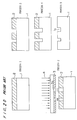
- FIG. 20 shows a conventional micro-fabrication process using photolithography.
- Step 1 a semiconductor substrate base 1 is coated with a photoresist material 2.
- Step 2 ultraviolet (UV) light 4 is irradiated through a photomask 3 to transfer the pattern holes 3a on the photomask 3 onto the photoresist coating 2.
- Step 3 through a development process, those areas of the photoresist material 2 which were exposed to the UV light 4 through the patterns holes 3a is removed.
- anisotropic etching is performed in Step 4 on those areas which are not protected by the photoresist coating 2.
- Step 5 is the removal of the photoresist coating.
- At least the above series of basic steps are required to produce cavities 1c of the same pattern as the pattern holes 3a of the photomask 3 on the surface of the substrate base 1.
- the usual practice for fabricating a semiconductor device is to repeat the above series of basic steps combined with introduction of dopants at selected stages of the photolithographic process.
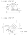
- a vacuum deposition process comprises the steps of: heating a target material 6 in a vacuum vessel 5 with a heater 6a; vaporizing the target material 6 to deposit a vapor on a workpiece 7, such as a substrate base, to be coated; depositing a film 6c by continuing the vaporizing and coating processes.
- the method of heating includes resistance heating, radiation heating and electron beam heating.
- a sputtered coating is formed by enclosing a substrate base 7 in a vacuum vessel, as shown in FIG. 32, and a high energy beam such as ion beams are radiated from a beam source 8 to a target source 9 and the sputtered particles 9a, which is a secondary emission product from the target source 9, are deposited on the substrate base 7 to form a sputtered coating 9b.
- the ion beam source is usually fixed on a flange and the degree of freedom of orientating the source is severely limited, consequently, it is difficult to position the beam source so that any surface of a workpiece may be irradiated, and it is especially difficult to employ a plurality of energy beam sources to perform a three-dimensional irradiation on the workpiece.
- Another problem in the conventional method is that if an ion beam source or electron beam source is used to remove a photoresist coating, in addition to having such beam sources, it is necessary to have a reactive gas supply facility. Further, the ion beam source or electron beam source is fixed to a flange, and as mentioned earlier, although a certain degree of movement of the workpiece is feasible, it is basically restricted to a two-dimensional fabrication task on one surface of the workpiece. It is even more difficult to perform fabrication on one selected spot of the subject using freely selectable beam sources and different incident beam angles.
- the conventional film deposit forming processes are designed to produce a pattern uniformly overall on a selected surface of a workpiece, and they are not suitable for producing desired patterns on selected surfaces or locations on the workpiece.
- the result is that it is difficult presently to produce a high performance assembled part from several microsized parts or to produce a film deposit on complex shaped articles.
- assembling of micro-parts or forming a film deposit on a complex shaped part requires that a deposit of a certain pattern is formed on a selected surface or on a restricted location of a workpiece, however, the conventional methods are designed for forming a film deposit of uniform characteristics, and is inadequate to meet the growing demand for a more flexible and adaptable device for performing micro-fabrication in a three-dimensional space.
- an energy beam source comprising: a discharge tube; a gas supply nozzle for supplying a process gas to the tube from upstream to downstream; a beam discharge nozzle having not less than one beam discharge opening; and not less than three electrodes disposed in the discharge tube; wherein each electrode of the not less than three electrodes is applied with an operating electrical voltage selected from a group consisting of a high frequency voltage, a direct current voltage and a ground voltage, and wherein the energy beam source supplies a beam having an adjustable energy level and a selectable species of particles chosen from a group consisting of positive ions, negative ions, highspeed neutral atoms, radical particles and electrons by suitably selecting operating parameters, including the operating electrical voltage, associated with each of the not less than three electrodes, and the process gas.
- the beam source is able to generate a beam having any one of positive ions, negative ions, highspeed neutral atoms, radical particles and electrons by selecting operating parameters, such as high frequency voltage, DC voltage and ground voltage, to be applied to a combination of electrodes. Therefore, a variety of micro-fabrication tasks can be performed using one beam source.
- the beam discharge nozzle is provided with not less than one beam discharge opening, wherein a diameter range of the beam discharge opening is selected from a group consisting of a 0.1 nm to 10 nm range, a 10 nm to 100 nm range and a 100 nm to 10 ⁇ m range, and wherein a length of the beam discharge opening is selected from a group consisting of a 1 to 5 times the diameter, 5 to 10 times the diameter, and not less than 10 times the diameter.
- the energy beam of an extremely fine size embodied by 0.1 nm - 10 ⁇ m, having an aspect ratio of the diameter to the length of the order of 1-10 can be generated.
- the efficiency of forming neutrally-charged atoms is improved, and highly efficient highspeed atomic beam can be generated.
- the energy beam source is a compact source, and not less than one of the beam sources is mounted on handling means, including a micro-manipulator and a rotation/translation stage, so as to provide a freedom in orienting the beam source in any orientation with respect to the workpiece.
- the energy beam source is made compact and is mounted on a micro-movement stage, it is possible to irradiate a specific local area of the workpiece to perform micro-fabrication tasks such as local deposit forming and etching.
- an electrode disposed in a farthest downstream location is provided with a patterned mask integrally formed with the electrode so as to permit a beam to pass through a patterned opening formed on the patterned mask.
- the beam source is provided with a patterned mask, the necessity for the photo-mask used in the conventional photolithography can be eliminated.
- the apparatus is provided with transport means for providing a relative movement of the workpiece and the energy beam source for performing micro-fabrication tasks, including local film deposition, local etching, bonding and attaching.
- two beam sources for example, can be used to perform different micro-fabrication tasks on any surface or location of the workpiece by suitably orienting the sources. Further, by focusing two kinds of beams on a local area of the workpiece, it is possible to achieve synergistic effects of different beams to achieve fabrication products which have not been possible heretofore.
- Additional object of the present invention is to provide a method of micro-fabrication using the various types of beam source presented above.
- a low-energy beam is used in association with a film-forming gas; the low-energy beam may be radiated on a workpiece; wherein a relative movement of the energy beam source and the workpiece is provided so as to produce any deposition pattern on any surface or any location on the workpiece.
- Another aspect of the method is that an electron beam is radiated on a workpiece through a patterned mask having a specific pattern; wherein a relative movement of the energy beam source and the workpiece is provided so as to produce any deposition pattern on any surface or any location on the workpiece.
- a coating of a film-forming material or supplying a film-forming gas may be applied on a surface of a workpiece; and the electron beam is radiated on the surface of the workpiece so as to activate film-forming particles to form a film deposit on the surface; wherein a relative movement of the energy beam source and the workpiece is provided so as to produce any deposition pattern on any surface or any location on the workpiece.
- highly directed electron beam can be radiated to activate the film-forming particles to form a local deposit, and the use of transport means enables to perform processing on any surface and any location of the workpiece.
- Another aspect of the method is that a coating of a film-forming material is applied or a film-forming gas is supplied on a surface of a workpiece; and an electron beam is radiated on the surface of the workpiece through a patterned mask having a specific pattern to form a film deposit on the surface; wherein a relative movement of the electron beam source and the workpiece is provided so as to produce any deposition pattern on any surface or any location on the workpiece.
- a pre-coated film-forming material or the particles of the film-forming gas is activated locally by the electron beam passing through the patterned mask, and the use of transport means enables to perform processing on any surface and any location of the workpiece.
- the final aspect of the method is that a coating of a film-forming material is applied or a film-forming gas is supplied on a surface of a workpiece; and an electron beam is radiated on the surface of the workpiece from a shaped electrode configured to a specific pattern to form a film deposit on the surface; wherein a relative movement of the electron beam source and the workpiece is provided so as to produce any deposition pattern on any surface or any location on the workpiece.
- a pre-coated film-forming material or the particles of the film-forming gas is activated by the highly directed electron beam from the shaped electrode, and the use of transport means enables to perform processing on any surface and any location of the workpiece.
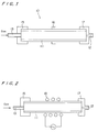
- FIG. 1 is a schematic illustration of a first embodiment of the energy beam source of the present invention.
- FIG. 2 is a schematic illustration of a second embodiment of the energy beam source of the present invention.
- FIG. 3 is a schematic illustration of a third embodiment of the energy beam source of the present invention.
- FIG. 4 is a schematic illustration of a fourth embodiment of the energy beam source of the present invention.
- FIG. 5 is a schematic illustration of a fifth embodiment of the energy beam source of the present invention.
- FIG. 6 is a schematic illustration of a sixth embodiment of the energy beam source of the present invention.
- FIG. 7 is a schematic illustration of a seventh embodiment of the energy beam source of the present invention.
- FIG. 8 is a schematic illustration of an eighth embodiment of the energy beam source of the present invention.
- FIG. 9 is a schematic illustration of a ninth embodiment of the energy beam source of the present invention.
- FIG. 10 is a schematic illustration of a tenth embodiment of the energy beam source of the present invention.
- FIG. 11 is a schematic illustration of an eleventh embodiment of the energy beam source of the present invention.
- FIG. 12 is a schematic illustration of a twelfth embodiment of the energy beam source of the present invention.
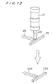
- FIG. 13 is a schematic illustration of a thirteenth embodiment of the energy beam source of the present invention.
- FIG. 14 is a schematic illustration of a fourteenth embodiment of the energy beam source of the present invention.
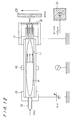
- FIG. 15 is a schematic illustration of a fifteenth embodiment of the energy beam source of the present invention.
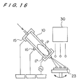
- FIG. 16 is a schematic illustration of a sixteenth embodiment of the energy beam source of the present invention.
- FIG. 17 is a schematic illustration of a micro-fabrication apparatus using a seventeenth embodiment of the energy beam source of the present invention.
- FIG. 18 is a schematic illustration of a micro-fabrication apparatus using an eighteenth embodiment of the energy beam source of the present invention.
- FIG. 19 is an illustration of the bonding step in FIG. 18.
- FIG. 20 is an illustration of a conventional process of photolithography.
- FIG. 21 is a perspective view of a nineteenth embodiment of the energy beam source of the present invention.
- FIG. 22 is a perspective view of a twentieth embodiment of the energy beam source of the present invention.
- FIG. 23 is a perspective view of a twenty-first embodiment of the energy beam source of the present invention.
- FIG. 24 is a perspective view of a twenty-second embodiment of the energy beam source of the present invention.
- FIG. 25 is a perspective view of a film deposit made by the fourth embodiment of the energy beam source.
- FIG. 26 is a perspective view of a twenty-third embodiment of the energy beam source of the present invention.
- FIG. 27 is a schematic block diagram to show an example of a system for performing the method of the present invention.
- FIG. 28 is a perspective view of a twenty-fourth embodiment of the energy beam source of the present invention.
- FIG. 29 is an illustration of the bonding step in FIG. 8.
- FIG. 30 is a schematic illustration of a twenty-fifth embodiment of the energy beam source of the present invention.
- FIG. 31 is an illustration of a conventional method of making a film deposit.
- FIG. 32 is an illustration of a conventional method of making a film deposit.
- Part I relates to Energy Beam Sources
- Part II relates to Methods of Micro-Fabrication using the energy beam sources of Part I.
- FIG. 1 is an energy beam source of the first embodiment.
- the energy beam source (shortened to source hereinbelow) 10 is placed in a vacuum vessel (not shown) together with a workpiece to be irradiated with the beam.
- the source comprises three electrodes 15, 16 and 17, the middle electrode 16 is ring-shaped, attached to a discharge tube 11 made of a pyrex glass or quartz.
- the source is designed so that a process gas stream is made to flow from an inlet (upstream) to an outlet (downstream).
- the downstream electrode 17 is provided with a beam discharge nozzle 12 having a beam discharge opening 12.
- the upstream electrode 15 is provided with a gas supply nozzle 13 for supplying a process gas to the interior of the discharge tube 11.
- the beam discharge opening may be singular or plural.
- the source is a compact source, and it is possible to generate a beam of different energy levels or particle types by adjusting the type and magnitude of the voltage to be applied on the electrodes 15, 16 and 17.
- a desired fabrication process such as etching, film deposition, bonding, attachment, can be performed on specified location of the workpiece.
- a highly reactive process gas such as chlorine, CCl4, SF6, CF4, O2 and chloro-fluoro hydrocarbons.
- process gases such as aluminum chloride, tungsten hexafluoride, methane, titanium chloride diluted with He and/or Ar gases are used.
- Bonding and attachment can be performed by aligning the workpiece with the source, before fabrication, using a light microscope, laser microscope and scanning electron microscope (SEM) and the like magnifying means.
- SEM scanning electron microscope
- FIG. 2 shows a second embodiment of the source.
- the basic configuration is the same as that in the first embodiment, but a coil 18, equivalent to the middle electrode 16, is disposed in the center of the discharge tube 11 for applying a high voltage to generate a plasma within the tube 11.
- the high frequency inductive discharge by the coil 18 generates a higher density plasma than the capacitively coupled type due to the formation of a magnetic field by the application of the high frequency voltage on the coil and the consequent activation of the electron activity by the magnetic field and their effect on the plasma generation (in the process gas supplied from the gas nozzle).
- the process gas is referred to as gas hereinbelow.
- FIG. 3 shows a third embodiment of the energy beam source.
- the middle electrode can be either a ring type 16 or a coil type 18, but in either case, the electrode is applied with a high frequency voltage.
- the remaining electrodes 15, 17 are grounded.
- a gas for forming the radical particles is introduced from a gas nozzle 13 disposed upstream, and a high frequency discharge plasma is formed within the tube 11.
- the radical particles formed in the plasma are accelerated by the pressure difference between the beam discharge opening 12 and the surrounding atmosphere, and are discharged through the beam to irradiate the workpiece disposed downstream.
- FIG. 4 shows a fourth embodiment of the energy beam source.
- the downstream electrode 17 is applied with a high frequency voltage.
- the middle electrode 16 is a ring electrode, and are grounded along with the upstream electrode 15.
- discharge occurs between the middle electrode 16 and the downstream electrode 17, and a plasma is generated in the downstream side of the discharge tube 11.
- Plasma radical particles are emitted from the beam discharge opening 12 due to the pressure differential between the interior and exterior of the tube 11 as in the previous embodiment.
- the high frequency voltage is applied, electron vibrational activities are generated near the beam discharge opening 12 also, and the radical particles become activated in this vicinity, thereby enabling to irradiate the workpiece with radical particles of a high activity.
- FIG. 5 shows a fifth embodiment of the energy beam source. This is an example of varying the voltage to be applied on the electrodes to generate highspeed atomic beam.
- a high frequency voltage is applied on the upstream electrode having a gas supply nozzle, the middle electrode 16 is grounded and the downstream electrode 17 is applied with a negative voltage. Therefore, discharge is generated by the two electrode on the upstream side of the tube 11, and a plasma is generated. The positive ions in the plasma are accelerated towards the downstream electrode 17, and perform charge exchange with the residual gaseous particles in the beam discharge opening 12, and are emitted as a neutral highspeed atomic beam.
- FIG. 6 shows a sixth embodiment of the energy beam source.
- a positive DC voltage is applied on the upstream electrode 15, and the high frequency voltage is applied on the middle electrode 16.
- the downstream electrode 17 is grounded.
- the middle electrode can be either a capacitively coupled type or an inductively coupled type. If it is capacitive, a ring electrode 16 is used, and if it is inductive, a coil electrode 18 is used.
- the acceleration biasing voltage between the electrodes 15, 17 is kept constant, and the electron activities is promoted by the high frequency voltage applied on the middle electrode 16 or 18, and a plasma is generated.
- the positive ions in the plasma are accelerated by the biasing voltage to be accelerated towards the downstream electrode 17 provided with a beam discharge opening 12, and are neutralized in the beam discharge opening 12.
- by impressing a positive voltage on the downstream electrode 17 and grounding the upstream electrode 15 it is possible to irradiate the workpiece with highspeed atomic beam of negative ions generated in the plasma.
- FIG. 7 shows a seventh embodiment of the energy beam source. This is an example of forming a local deposit or bonding using any of the sources presented above.
- a radical discharge nozzle 19 is provided on the tip of the downstream electrode to form a local deposit.
- the radical discharge nozzle 19 has an inside diameter of 0.1-0.3 mm and is provided with a thin plate 20 having an opening of 0.1 nm-10 ⁇ m at a tip.
- FIG. 8 shows an eighth embodiment of the energy beam source.
- a patterned mask 21 is integrally provided at the tip end of the downstream electrode.
- the patterned mask 21 is provided with a pattern having certain shapes or fine holes. This is used when the beam discharge opening 12 is too large or when there are several of them, to block a part of the beam downstream by passing the beam through the pattern hole 22 before the workpiece 23 is irradiated. This is useful when the sputtered particles in the downstream side produce an undesirable effect on the workpiece 23.
- FIG. 9 is a ninth embodiment of the energy beam source.
- a workpiece 23 is assembled with a small rod 24, and a local deposit is formed in the assembled section to provide reinforcement of the assembled section.
- the diameter of the small rod 24 is about 10 nm-100 ⁇ m.
- a cavity was produced on the workpiece 23 with the highspeed atomic beam produced from the energy beam source presented above, and the rod was positioned in the hole by means of a micro-handling apparatus.
- the local deposition was made either by changing the applied voltage setting or by using another energy source.
- Highspeed atomic beam was radiated on the assembled section to provide reinforcement to the attachment/bonding at the assembled section.
- FIG. 10 is a tenth embodiment of the energy beam source.
- a patterned mask 21 is provided integrally with the downstream electrode 17.
- Highspeed atomic beam discharged from the beam discharge opening is shaped by the mask 21 according to a micro-sized pattern provided on the mask 21 and is radiated on the workpiece 23.
- the micro-sized holes on the mask 21 range between 0.1 nm-100 ⁇ m, and can have any type of patterns.
- the workpiece 23 is disposed on a movable stage (not shown), and the energy beam source side is fixed. Therefore, by moving the workpiece relative to the fixed radiation position of the source, it is possible to generate line, dot and other patterns or to perform micro-sized etching of some fine patterns.
- FIG. 11 shows an eleventh embodiment of the energy beam source.
- this embodiment there are a plurality of beam discharge openings 12 provided on the downstream electrode 17.
- This source is used when there is a need for a large diameter beam. It is also useful for suppressing the undesirable effects on etching which may be caused by the sputtered particles from the downstream electrode 17.
- it is also effective to provide a quartz plate or a coating of oxides of silicon on the inside of the downstream electrode 17.
- FIG. 12 shows a twelfth embodiment of the energy beam source.
- the configuration of this embodiment is almost the same as that of the eleventh embodiment, however, in the eleventh embodiment, the high frequency voltage was applied to the upstream electrode 15 and a plasma was generated between the upstream electrode 15 and the middle electrode 16, in comparison, in this embodiment, the upstream electrode 15 is applied with a DC voltage, and the high frequency voltage is applied on the middle electrode 16.
- This configuration produces a plasma through the entire discharge tube 11.
- FIG. 13 shows a thirteenth embodiment of the energy beam source. This is an example of performing a localized deposition process using any of the sources presented above.
- a junction of two continuous wiring 25 is severed locally by using a highspeed atomic beam 26 from a fine diameter energy beam source 10.
- the connection is now divided into two separate wiring 25A, 25B. This method is applicable to severing aluminum wiring deposited on a semiconductor substrate base, circuit wiring on printed circuits and micro-wiring on quantum devices and the like.
- FIG. 14 is a fourteenth embodiment of the energy beam source.
- local etching on a workpiece 23 is performed by a radical particle beam 27 from a source 10.
- the example is a case of moving the workpiece 23 while irradiating the workpiece 23 with the radical particle beam 27 to provide local etching on the workpiece 23.
- the relative movement can be provided by either the source or the workpiece.
- FIG. 15 is a fifteenth embodiment of the energy beam source.
- This embodiment is an example of performing a localized deposition process on a separated wiring or spaces between fine structures by using radical particle beam in conjunction with film forming gases(s).
- the space between the separated wiring 25A and 25B is irradiated with a radical particle beam 27 from a source 10 to form a local deposit 29 to provide an electrical connection between the wiring 25A and 25B to provide an electrical path 25.
- FIG. 16 shows a micro-fabrication apparatus using an energy beam source of the sixteenth embodiment.
- a source 10 is used in conjunction with another source 30. This is an example of using a highspeed atomic beam 30 and a radical particle beam 10.
- the combined action of the atomic beam from the highspeed atomic beam 30 and the radical particle beam from the radical particle source 10 offers an opportunity to increase the etching performance significantly.
- the combined effects of the increased reactivity offered by the radical particle beam and the selection capability of local fabrication offered by the highspeed atomic beam are able to provide both an increased etching speed as well as an accurate anisotropic local fabrication.
- FIG. 17 shows a fabrication apparatus using a seventeenth embodiment of the energy beam source. This is an example of an apparatus for performing different tasks, such as etching and film deposition, on different surfaces of a workpiece 23 using a plurality of energy beam sources.
- a highspeed atomic beam source 30 is positioned, and radiates a highspeed atomic beam on a top surface of a workpiece 23 through a mask 21.
- This example relates to etching of a top surface of the workpiece 23 with an atomic beam passing through the opening of the mask 21, and the pattern projected on the surface is the pattern provided at the opening, thereby performing the tasks of pattern duplication and etching of the pattern simultaneously.
- a compact energy beam source 10A is a radical particle source, and supplies radical particles from an inclined top location to an irradiated local spot of the highspeed atomic beam source 30. At the local spot, the etching rate is increased significantly due to the interactive effect of the highspeed atomic beam and the radical particles, and a cavity having steep side walls, for example, is produced at a high etching rate.
- a compact source 10C moves while radiating a highspeed atomic beam thereon to perform an etching task to produce an extended channel along the side surface.
- a compact source 10B radiates a radical particle beam generated from a film deposition gas, and the movement of the beam along the side surface produces a fine extended (protrusion) deposit on the side surface.
- the sources 10A, 10B and 10C and the like are disposed respectively on a manipulator or other rotation/translation stages to permit movement precision of a nm order.
- the beam is capable of producing patterns of the order of nm sizes, as described earlier. Therefore, by utilizing a plurality of sources disposed in such a way to permit irradiating a workpiece from a plurality of directions, it is possible to produce extremely fine patterns in a three-dimensional space.
- the example related to a case of fabricating different patterns on three surfaces, but it is also possible to carry out sequential fabrication following a certain sequencing schedule. It is naturally permissible to carry out one type of fabrication on each surface of a workpiece.
- the sources 10A, 10B and 10C are able to perform different processes, such as etching and film deposition, by choosing suitable operating voltages to be applied on the upstream, middle and downstream electrodes and selecting suitable process gas species to be admitted into the discharge tube. For example, a process schedule such as light etching of a side surface to expose a clean surface, followed by depositing of a fine line protrusion on the cleaned surface can readily be carried out using the source of this invention.
- the source is designed to have at least three electrodes each of which can be applied with a DC voltage, a high frequency voltage or a ground voltage.
- the electrode to be used for high frequency voltage application includes the capacitively coupled type or inductively coupled type.
- the inductively coupled type uses a coil electrode.
- the high frequency source is not particularly limited, and the choice being made on the basis of end application, and usually a frequency of 13.56 Hz is employed.
- the use as a radical particle source would require the downstream or middle electrode to be applied with a high frequency voltage so that the generated radical particles would be accelerated due to the pressure differential and discharged from the beam discharge opening.
- the energy beam source enables to select whether to accelerate the positive ion particles or negative ion particles in the plasma by applying either a high voltage or a low voltage on the beam discharge electrode.
- the accelerated ion particles undergo charge exchange with the residual gas particles in the beam discharge opening, and are emitted therefrom as a highspeed atomic beam containing neutral charge particles.
- the dimensions of the beam discharge opening diameter and its length, providing an aspect ratio of the discharge opening, are critical factors in determining the properties of the energy beam.
- the diameter of the beam discharge opening is important, and for this purpose the diameter must be in ranges of 0.1-10 nm, 10-100 nm or 100 nm-10 ⁇ m.
- the length of the opening significantly affects the character of the discharged beam, and therefore, the length must also be chosen to suit the application. For example, when the length is within 1-5 times the diameter of the opening, the highspeed atomic beam comprises electrons, ions, radicals and moderately neutral particles.
- the discharge beam expands downstream so that it is possible to irradiate a circular area of 10-50 times the diameter of the opening.
- the directionality of the beam is excellent, and it is possible to localize the irradiation area.
- the neutralization factor of the high-speed atomic beam within the opening is increased to about 30-70 % of the total particles.
- the beam directionality is further improved and the neutralization factor is also increased to about 70 %. This type of highspeed atomic beam is excellent for fabrication of an extremely fine localized area.
- the source is designed to be compact and the operating parameters can be freely varied by selecting an appropriate operating voltage to be applied on the electrodes.
- the electrodes are connected to lead-in terminals of the vacuum vessel which are connected through flexible coaxial cables to an outside control unit on the atmospheric side. Therefore, by simply changing the input terminal cables, it is possible to select the type of voltage to be applied on the electrode, thereby providing a beam of desired energy level and particle type.
- the source located inside the vacuum vessel may be singular or plurality, and may be mounted on a manipulator or rotation/translation stage so as to permit various types of fabrications to be carried out, such as etching, film deposition, bonding and attaching, either simultaneously or serially on any surface of a workpiece.
- the workpiece itself may be mounted on a manipulator or rotation/translation stage so as to perform fabrication on a plurality of workpiece surfaces.
- the manipulator or rotation/translation stage is designed so that it may be operated from the outside control unit.
- the source can be used to perform local fabrication, such as local film deposition/etching and the like, or bonding/attaching of more than two fine objects.
- a mask having micro-patterns is disposed integrally on a downstream beam source, thereby enabling to transfer patterns on a workpiece without using conventional photomasking and the like.
- Such an integral masking is useful in preventing undesirable effects of sputtered particles generated from the discharge electrode in the discharge tube. This can be prevented by having a plurality of beam discharge openings to reduce the amount of sputtered particles, and carrying out the local fabrication with the use of the integral patterned mask to control the beam shape and diameter.
- positioning and fabrication of a plurality of fine workpieces may be carried out under a light microscope, laser microscope, SEM and the like magnifying means.
- FIGS. 18 and 19 show a method of performing three-dimensional fabrication of a workpiece using an eighteenth embodiment of the energy beam source.
- assembly operation may involve, for example, making openings 23A, 23B using the source 10A, 10B.
- the workpiece 23 is a silicon single crystal or a polyamide resin.
- a manipulator 31 is used to insert a rod piece 33 made of stainless steel of 300 ⁇ m diameter, for example, into the opening 23A.
- a plate piece 33B is inserted using the manipulator 31. Bonding operation may require revolving of the source 10A in a cone shape around the workpiece 23 and radiating a reactive radical particle beam to the joint area between the opening 23A and the rod piece 33.
- the reactive radical particle beam is radiated on the joint between the plate piece 33B and the opening 23B. Irradiation with the reactive radical particle beam produces a bonding agent 34, a local film deposit, at the joint area to join two different materials, thereby bonding the workpiece 23 to the rod piece 33A and the plate piece 33B.
- FIG. 19 illustrates the process of inserting the rod piece 33A into the opening 23A and irradiating the joint area with the radical particle beam to provide the bonding agent 34 for bonding the two pieces.
- Aligning of the insertion pieces and the beam is carried out while observing the pieces under a SEM or light microscope and operating a manipulator or a rotation/translation stage, capable of providing micro-alignment, having the insertion object or the source mounted thereon.
- the compact source is mounted on a rotation/translation stage, and irradiates the joint area with a beam oriented at a suitable angle.
- the position of the source may be fixed, and the pieces may be mounted on a rotation/translation stage.
- the beam source for such a fine diameter beam may be a film-forming type of reactive radical particle beam or low-energy highspeed atomic beam.
- a radical beam having carbon (C) particles is generated, and the bonding agent 34 formed may be graphite or diamond-like carbon.
- the process gas may include tungsten fluoride, aluminum chloride, titanium chloride and the like gases containing metallic component(s) or carbon group or hydrocarbon group gases and the like process gases containing C or C-H.
- the bonding agent formed at the joint area includes a film deposit of tungsten, aluminum, titanium, graphite, diamond-like carbon and polymeric films containing hydrocarbons. This is an example of the method of joining components of two different materials, which are mostly carried out under a vacuum.
- the traditional photolithographic method involves steps which are cumbersome because of the necessity of preparing photoresist patterns requiring such steps as rinsing, resist coating, exposure, baking and development of the image. There are occasions when uniform resist patterns cannot be made because of the problems in roughness and flatness of the substrate base.
- the method without using photoresist there is a problem of limited degree of freedom in fabrication patterns, and only one pattern is made for one device design, so if a different pattern is needed, another pattern must be generated to undertake photolithography.
- the degree of freedom in fabrication such as pre-viewing the surface condition of an wafer, and deciding on the regions to be used for fabrication or a three-dimensional fabrication on a workpiece, has been impossible.
- the conventional sources of ion or electron beams are fixed on a flange of a vacuum vessel, and although certain degree of control over the irradiation area is possible by moving the workpiece, it is limited basically to a two-dimensional movement. Furthermore, when performing etching or film deposition, a separate gas supply facility must be made available, and because the number of reactive gas particles is few, fast fabrication speed cannot be expected.
- the compact beam source can be used as a radical particle beam source or as a highspeed atomic beam source. Because the relative alignment of the radical beam source or highspeed atomic beam source can be controlled with the use of a manipulator or a rotation/translation stage, it is possible to perform any desired fabrication on any surface of a workpiece. Because the source is a compact source, a plurality of sources may be utilized simultaneously or serially to perform different fabrication operations on the same surface of the workpiece. Because the source is capable of radiating a reactive process gas directly, the fabrication speed is much faster than those utilizing a separate ion beam or electron beam in conjunction with a gas feed facility.
- beam discharge opening can be selected to suit the application requirements, for example, in three ranges of 0.1-10 nm; 10-100 nm; and 100 nm to 10 ⁇ m. It is also possible to use a masking having the desired holes or patterns integrally provided on an energy beam source for use in fabricating local areas of a workpiece. Localized etching, film deposition, bonding and attaching process can be undertaken to realize a fabrication of a three-dimensional structure which has been extremely difficult using the conventional approach. The availability of the compact energy beam source has thus opened a new path to such leading-edge industries as repair of semiconductor devices, circuit alteration/repair and micro-machining of ultrasmall components for medical devices.
- FIG. 21 shows a nineteenth embodiment of the present invention.
- This embodiment relates to a method of forming a film deposit 47 by irradiating a workpiece 45 with a low-energy beam 41, in association with a film forming gas, through a mask 43 having a hollowed-out pattern to produce a film deposit 47 of the same design on the workpiece 45.
- the low-energy beam 41 includes low-energy atomic beam, ion beam, molecular beam and atomic beam and the like beams associated with film-forming gases.
- the energy levels may range between 0.1-200 eV, and the beam diameter may range between 1 ⁇ m to 300 mm.
- the mask 43 may include electro-formed patterned masks, wet etched stainless steel masks, excimer-laser fabricated masks or higher precision masks such as Ni masks produced by laser ionic gas attack (LIGA) process.
- LIGA laser ionic gas attack
- Film-forming gas can be chosen to suit the workpiece but may include methane, aluminum chloride, silicon tetrachloride, tungsten fluoride suitably diluted with argon or helium.
- the films which can be made by the method include metals, ceramics, resins and polymers and their composite material, and the process gas may be any gas or vapor of appropriate compositions.
- the deposition process of making a film deposit 47 comprises main steps of aligning and mask 43 with the workpiece 45 mounted on a positioning devices 49, 51 (for distance, parallelism and relative positioning etc.); irradiating the workpiece 43 with the low-energy beam 41 through the openings on the mask 43.
- the illustration shows the mask 43 is moved along the X-, Y- and Z-axes and the workpiece is moved along the X- and Y-axis, but the mask and the workpiece may be rotated about at least one of the X- and/or Y-axis. It is not necessary that both workpiece and the mask are moved, but only one of them can be moved.
- FIG. 22 shows a twentieth embodiment which uses an electron beam as a low-energy beam 41a.
- a film-forming material 53 may be precoated on the surface of the workpiece 45 or a film-forming gas 55 may be supplied with the electron beam 41a.
- the film-forming material 53 or directing the film-forming gas on the surface of the workpiece 45, and radiating the electron beam 41a through the mask 43, the film-forming material or the film-forming gas are activated on the surface of the workpiece, and a deposit 47 having the same pattern as the mask is produced on the workpiece.
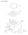
- FIG. 23 shows a twenty-first embodiment which provides a multi-axial movement.
- a workpiece 45a disposed on a positioning device (not shown) is translated along X- and Y-axes as well as rotated about the X- and Y-axes so as to produce a film deposit 47 on any surface or any location of the workpiece 45a.
- the workpiece 45a can also be moved along the Z-axis or rotated about the Z-axis.
- the beam source 40 and/or the mask can be translated at least along one axis of the X-, Y- and Z-axes as well as rotated about one of the X-, Y- and Z-axes with the workpiece located at the center of revolution.
- a film-forming material 53 may be coated on the workpiece 45a beforehand or use a film-forming gas along with the electron beam, as in the case described for the embodiment in FIG. 22.
- FIG. 24 shows a twenty-second embodiment.
- the radiation is a converging beam 41b which is irradiated directly onto the workpiece 45a without using a mask.
- the workpiece 45a is mounted on a positioning device (not shown) and is translated along and rotated about the X-and Y-axes, and the beam source 40 is rotatable about the X-and Y-axes.
- the diameter of the converging beam includes a 0.1-10 nm range; a 10 nm - 1 ⁇ m range; or a 1-100 ⁇ m range, and preferably a 10 nm - 1 ⁇ m range.
- a film-forming material may be coated on the workpiece beforehand or a film-forming gas may be directed along with the electron beam.
- FIG. 25 illustrates an example of using the method of forming a film deposit shown in FIG. 24 to produce a film deposit 47 having the desired pattern on a surface of a complex shaped, stepped workpiece made by assembling two micro-parts 45b, 45c.
- FIG. 26 shows a twenty-third embodiment.
- the beam 41c radiated from a beam source 40 has a certain shape, and the workpiece 45 is able to translate along as well as rotate about the X- and Y-axes. Therefore, without using a mask, a film deposit 47 having any desired pattern may be formed on any surface or location of the workpiece 45a. Shaped-beam can be generated by shaping the electrode 40a of the beam source 40 in the desired pattern.
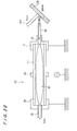
- FIG. 27 shows an example of a system for forming a film deposit according to the present invention.
- the workpiece 45 is able to translate along the X- and Y-axes by means of an XY-stage 59 as well as rotate about the X- and Z-axes passing through the center of the workpiece 45 by means of a rotation device 61, 63 provided on the X-Y stage 59.
- the beam source 40 is able to translate along as well as rotate about the X-, Y- and Z-axes by means of a manipulator 73 including an XY-stage 65, a Z-stage 67 and the rotation devices 69, 71.
- the beam source 40 has a converging beam having a diameter of 0.1 nm - 100 ⁇ m.
- a non-convergent beam having a beam diameter of 1 ⁇ m - 300 mm may be used.
- a magnifying means 75 such as a light microscope, laser microscope or SEM and the like may be used to provide accurate information on film location and deposition conditions.
- Film deposition process is generally performed in an evacuated vessel 77 having an XY-stage 59 for holding the workpiece, a manipulator 73 for the beam source and a magnifying means 75 disposed therein, and the process control, such as positioning of the workpiece and the beam source, is carried out from outside the vessel 77.
- FIGS. 28 and 29 show a twenty-fourth embodiment relating to a method of micro-fabrication in a three-dimensional space.
- stage A micro-sized opening 82A, 82B are formed on a workpiece 81 using a beam sources 80A, 80B.
- the workpiece 81 may be represented by a silicon single crystal or a polyamide resin material.
- stage B a rod piece 85 of a 300 ⁇ m diameter stainless steel, for example, is insertingly coupled into the opening 82A using a manipulator 84A.
- a plate piece 86 of a silicon single crystal for example, is insertingly coupled into the opening 82B using a manipulator 84B.
- stage C the joint area between the rod piece 85 and the opening 82A is irradiated with a radical particle beam of a reactive gas generated from a beam source 80A which is rotated in a path of a cone shape about the Z-axis as illustrated in FIG. 28, stage C.
- the joint area between the plate piece 86 and the opening 82B is irradiated with a radical particle beam source by moving the beam source 80B parallel to the surface of the workpiece 81.
- the irradiation process with the radical particle beam produces a bonding agent 87 to bond different materials, manifested in this embodiment by the workpiece 81, the rod piece 85 and the plate piece 86.
- FIG. 29 is an illustration of the process of irradiating the joint area with a radical particle beam to form a local bonding agent (deposition) 87 between the workpiece 81 and the inserted rod piece 85.
- FIG. 30 shows a twenty-sixth embodiment in which different materials are joined with the use of a high frequency plasma beam.
- a beam source 10 comprises a discharge (insulating) tube 11, an upstream electrode 15 and a downstream electrode 17 both of which are grounded, and a middle electrode 16 which is applied with a high frequency voltage. It is permissible to apply a positive voltage to the upstream electrode 15.
- the middle electrode 16 may be a capacitively coupled type or an inductively coupled type, and if capacitively coupled, a ring electrode is used, and if inductively coupled, a coil electrode is used.
- a plasma is generated by promotion of the vibrational action of the electrons by the application of a high frequency voltage on the middle electrode 16.
- the positive ions in the plasma are accelerated by the biasing acceleration voltage towards the beam discharge opening 12 of downstream electrode 17, and are neutralized therein.
- the downstream electrode is provided at its tip with a radical particle discharge nozzle 19 for forming a local film deposit.
- the radical particle discharge nozzle 19 disposed at the tip has an inside diameter of 0.1-3 mm, and may be provided with a screen hole of 0.1 nm - 10 ⁇ m for forming a fine stream of radical particles.
- This embodiment illustrates a case of inserting a micro-sized rod piece 24 into a workpiece 23 followed by forming a local film deposit to bond the rod piece 24 to the workpiece 23.
- the diameter of rod piece 24 ranges between 10 nm - 100 ⁇ m.
- Typical processing stages are as follows. Insertion cavities are produced by the highspeed atomic beam generated in the beam source apparatus shown in FIG. 28, the component pieces are assembled into the cavities while observing the assembly under magnifying means using micro-handling means, and the beam source is positioned on the joint area for local film deposition.
- the beam source in this case may be obtained by changing the parameters of the same electrode, or may utilize another beam source.
- a radical beam source is used to deposit a local bonding agent on the joint area as illustrated in FIG. 30.
- Aligning of the assembly pieces and positioning of the beam source with the workpiece are carried out under magnifying means such as a light microscope or SEM using a micro-handling device or a micro-handling stage, capable of providing the micro-movements suitable for the task, to which the beam source and/or the workpiece is mounted.
- magnifying means such as a light microscope or SEM using a micro-handling device or a micro-handling stage, capable of providing the micro-movements suitable for the task, to which the beam source and/or the workpiece is mounted.
- the beam source was mounted on a rotation/translation stage to permit irradiation at any orientation angle.
- the micro-beam source for micro-fabrication of a workpiece may be any of a reactive radical particle beam of a film-forming material or a low-energy highspeed atomic beam.
- the process gas for the beam source is methane, carbon (C) containing radicals are formed, and the bonding agent 67 formed includes graphite and diamond-like carbon.
- process gases include tungsten fluoride, aluminum chloride, titanium chloride and the like gases containing metallic component(s) or carbon or hydrocarbon group gases containing C or C-H.
- the bonding agent formed at the joint area includes films of tungsten, aluminum, titanium, graphite, diamond-like carbon and polymeric films containing hydrocarbons. This type of forming a film deposit of a bonding agent for bonding two different materials is carried out mostly in a vacuum environment.
- micro-fabrication method of the present invention is able to produce a three-dimensional structure of any material without encountering any such problems.
- FIGS. 21 to 30 it is preferable that all the fabrication methods presented in FIGS. 21 to 30 to be carried out in a vacuum environment, and micro- fabrication tasks under a magnifying means.
- the beam source, mask and the workpiece were translated along or rotated about the orthogonally intersecting axes. However, it is clear that they may be moved along axes which may be intersecting at oblique angles.
Landscapes
- Physics & Mathematics (AREA)
- Spectroscopy & Molecular Physics (AREA)
- Engineering & Computer Science (AREA)
- Plasma & Fusion (AREA)
- Chemical & Material Sciences (AREA)
- Analytical Chemistry (AREA)
- Chemical Vapour Deposition (AREA)
- Drying Of Semiconductors (AREA)
- Welding Or Cutting Using Electron Beams (AREA)
Applications Claiming Priority (4)
| Application Number | Priority Date | Filing Date | Title |
|---|---|---|---|
| JP252311/94 | 1994-10-18 | ||
| JP25231194 | 1994-10-18 | ||
| JP5323195 | 1995-02-17 | ||
| JP53231/95 | 1995-02-17 |
Publications (1)
| Publication Number | Publication Date |
|---|---|
| EP0710057A1 true EP0710057A1 (fr) | 1996-05-01 |
Family
ID=26393947
Family Applications (1)
| Application Number | Title | Priority Date | Filing Date |
|---|---|---|---|
| EP95116425A Withdrawn EP0710057A1 (fr) | 1994-10-18 | 1995-10-18 | Source de faisceau énergétique et procédé de dépÔt de film utilisant une telle source |
Country Status (2)
| Country | Link |
|---|---|
| US (2) | US5989779A (fr) |
| EP (1) | EP0710057A1 (fr) |
Cited By (5)
| Publication number | Priority date | Publication date | Assignee | Title |
|---|---|---|---|---|
| WO2001025504A1 (fr) * | 1999-10-07 | 2001-04-12 | Japan Science And Technology Corporation | Microstructure tridimensionnelle, son procede et dispositif de fabrication |
| WO2003002779A1 (fr) * | 2001-06-29 | 2003-01-09 | Nec Corporation | Procede de formage de structure de carbone diamantoide elastique ultra-resistante |
| EP1220272A4 (fr) * | 1999-07-14 | 2007-04-11 | Ebara Corp | Source de faisceaux |
| EP2048691A3 (fr) * | 2007-10-09 | 2009-12-23 | NTG Neue Technologien GmbH & Co. KG | Dispositif d'usinage de pièces par faisceau, installation de traitement par faisceau ionique |
| US20110174974A1 (en) * | 2000-11-02 | 2011-07-21 | Hitachi, Ltd. | Method and apparatus for processing a microsample |
Families Citing this family (30)
| Publication number | Priority date | Publication date | Assignee | Title |
|---|---|---|---|---|
| US6105885A (en) * | 1998-04-03 | 2000-08-22 | Advanced Energy Systems, Inc. | Fluid nozzle system and method in an emitted energy system for photolithography |
| US6905623B2 (en) * | 2000-12-15 | 2005-06-14 | Credence Systems Corporation | Precise, in-situ endpoint detection for charged particle beam processing |
| JP2002289585A (ja) * | 2001-03-26 | 2002-10-04 | Ebara Corp | 中性粒子ビーム処理装置 |
| US6680456B2 (en) | 2001-06-09 | 2004-01-20 | Honeywell International Inc. | Ion fusion formation |
| US20050103272A1 (en) * | 2002-02-25 | 2005-05-19 | Leo Elektronenmikroskopie Gmbh | Material processing system and method |
| US6891170B1 (en) * | 2002-06-17 | 2005-05-10 | Zyvex Corporation | Modular manipulation system for manipulating a sample under study with a microscope |
| US6932865B2 (en) * | 2003-04-11 | 2005-08-23 | Lockheed Martin Corporation | System and method of making single-crystal structures through free-form fabrication techniques |
| US7261779B2 (en) * | 2003-06-05 | 2007-08-28 | Lockheed Martin Corporation | System, method, and apparatus for continuous synthesis of single-walled carbon nanotubes |
| WO2005031789A2 (fr) * | 2003-09-23 | 2005-04-07 | Zyvex Corporation | Procede, systeme et dispositif pour examen microscopique faisant appel a un element de prehension destine a capturer un echantillon prepare par fib |
| US7262385B2 (en) * | 2004-01-28 | 2007-08-28 | The Boeing Company | Material processing device |
| TW200531420A (en) | 2004-02-20 | 2005-09-16 | Zyvex Corp | Positioning device for microscopic motion |
| US7285778B2 (en) | 2004-02-23 | 2007-10-23 | Zyvex Corporation | Probe current imaging |
| US7326293B2 (en) * | 2004-03-26 | 2008-02-05 | Zyvex Labs, Llc | Patterned atomic layer epitaxy |
| US7037882B2 (en) * | 2004-05-05 | 2006-05-02 | Bba Nonwovens Simpsonville, Inc. | Composition and material for cleaning printing machines |
| WO2006017510A2 (fr) * | 2004-08-02 | 2006-02-16 | J.P. Sercel Associates, Inc. | Systeme et procede d'usinage laser |
| KR101355280B1 (ko) * | 2004-08-24 | 2014-01-27 | 셀라 세미컨덕터 엔지니어링 라보라토리스 리미티드 | 워크피스를 밀링하기 위해 이온빔을 지향시키고 다수회 편향시키고, 그 정도를 결정 및 제어하기 위한 방법, 장치 및 시스템 |
| JP2006208104A (ja) * | 2005-01-26 | 2006-08-10 | Toyo Ink Mfg Co Ltd | 電子線照射装置および電子線照射方法 |
| US20100227523A1 (en) * | 2007-09-14 | 2010-09-09 | Exogenesis Corporation | Methods for improving the bioactivity characteristics of a surface and objects with surfaces improved thereby |
| US9144627B2 (en) * | 2007-09-14 | 2015-09-29 | Exogenesis Corporation | Methods for improving the bioactivity characteristics of a surface and objects with surfaces improved thereby |
| WO2010105102A1 (fr) * | 2009-03-11 | 2010-09-16 | Exogenesis Corporation | Procédés d'amélioration des caractéristiques de bioactivité d'une surface et objets avec surfaces améliorées de la sorte |
| EP2567012B1 (fr) * | 2010-05-05 | 2015-12-16 | Exogenesis Corporation | Procédés d'amélioration des caractéristiques de bioactivité d'une surface et objets ayant des surfaces améliorées par ce procédé |
| US10202684B2 (en) | 2010-08-23 | 2019-02-12 | Exogenesis Corporation | Method for neutral beam processing based on gas cluster ion beam technology and articles produced thereby |
| US9799488B2 (en) | 2010-08-23 | 2017-10-24 | Exogenesis Corporation | Method and apparatus for neutral beam processing based on gas cluster ion beam technology |
| CN103180030B (zh) * | 2010-08-23 | 2017-04-12 | 艾克索乔纳斯公司 | 基于气体团簇离子束技术的中性射束处理方法和设备 |
| US20180090295A1 (en) * | 2010-08-23 | 2018-03-29 | Sean R. Kirkpatrick | Drug delivery system and method of manufacturing thereof |
| US10825685B2 (en) | 2010-08-23 | 2020-11-03 | Exogenesis Corporation | Method for neutral beam processing based on gas cluster ion beam technology and articles produced thereby |
| EP2707598A4 (fr) * | 2011-05-12 | 2015-04-29 | Roderick William Boswell | Micro-propulseur à plasma |
| US10225919B2 (en) * | 2011-06-30 | 2019-03-05 | Aes Global Holdings, Pte. Ltd | Projected plasma source |
| US9315798B2 (en) | 2011-08-22 | 2016-04-19 | Exogenesis Corporation | Methods for improving the bioactivity characteristics of a surface and objects with surfaces improved thereby |
| EP2594357A1 (fr) * | 2011-11-16 | 2013-05-22 | Optec S.p.A. | Dispositif et procédé pour souder au laser avec une unité de calibration avec des éléments réfractants |
Citations (6)
| Publication number | Priority date | Publication date | Assignee | Title |
|---|---|---|---|---|
| US4510386A (en) * | 1981-03-31 | 1985-04-09 | Ion Tech Limited | Thinning of specimens for examination under the electron microscope |
| US4874459A (en) * | 1988-10-17 | 1989-10-17 | The Regents Of The University Of California | Low damage-producing, anisotropic, chemically enhanced etching method and apparatus |
| EP0497227A2 (fr) * | 1991-01-28 | 1992-08-05 | Sarcos Group | Méthode et appareil pour la fabrication de micro-structures utilisant la lithographie non planaire par exposition à un faisceau |
| US5149973A (en) * | 1990-07-02 | 1992-09-22 | Mitsubishi Denki Kabushiki Kaisha | Apparatus for wiring semiconductor device using energy beam and wiring method by using the same |
| EP0531949A2 (fr) * | 1991-09-12 | 1993-03-17 | Ebara Corporation | Source de faisceau d'atomes rapides |
| EP0639939A1 (fr) * | 1993-08-20 | 1995-02-22 | Ebara Corporation | Source de faisceaux d'atomes rapides |
Family Cites Families (12)
| Publication number | Priority date | Publication date | Assignee | Title |
|---|---|---|---|---|
| US4128765A (en) * | 1976-10-29 | 1978-12-05 | Joseph Franks | Ion beam machining techniques and apparatus |
| US4324854A (en) * | 1980-03-03 | 1982-04-13 | California Institute Of Technology | Deposition of metal films and clusters by reactions of compounds with low energy electrons on surfaces |
| US4505949A (en) * | 1984-04-25 | 1985-03-19 | Texas Instruments Incorporated | Thin film deposition using plasma-generated source gas |
| US4775789A (en) * | 1986-03-19 | 1988-10-04 | Albridge Jr Royal G | Method and apparatus for producing neutral atomic and molecular beams |
| US4793908A (en) * | 1986-12-29 | 1988-12-27 | Rockwell International Corporation | Multiple ion source method and apparatus for fabricating multilayer optical films |
| US4757179A (en) * | 1987-01-16 | 1988-07-12 | E. I. Du Pont De Nemours And Company | Laser welding method |
| JPH01132033A (ja) * | 1987-11-17 | 1989-05-24 | Hitachi Ltd | イオン源及び薄膜形成装置 |
| JP2650930B2 (ja) * | 1987-11-24 | 1997-09-10 | 株式会社日立製作所 | 超格子構作の素子製作方法 |
| US5135695A (en) * | 1989-12-04 | 1992-08-04 | Board Of Regents The University Of Texas System | Positioning, focusing and monitoring of gas phase selective beam deposition |
| US5223692A (en) * | 1991-09-23 | 1993-06-29 | General Electric Company | Method and apparatus for laser trepanning |
| US5468595A (en) * | 1993-01-29 | 1995-11-21 | Electron Vision Corporation | Method for three-dimensional control of solubility properties of resist layers |
| US5554853A (en) * | 1995-03-10 | 1996-09-10 | Krytek Corporation | Producing ion beams suitable for ion implantation and improved ion implantation apparatus and techniques |
-
1995
- 1995-10-17 US US08/544,108 patent/US5989779A/en not_active Expired - Fee Related
- 1995-10-18 EP EP95116425A patent/EP0710057A1/fr not_active Withdrawn
-
1999
- 1999-04-28 US US09/300,844 patent/US5998097A/en not_active Expired - Fee Related
Patent Citations (6)
| Publication number | Priority date | Publication date | Assignee | Title |
|---|---|---|---|---|
| US4510386A (en) * | 1981-03-31 | 1985-04-09 | Ion Tech Limited | Thinning of specimens for examination under the electron microscope |
| US4874459A (en) * | 1988-10-17 | 1989-10-17 | The Regents Of The University Of California | Low damage-producing, anisotropic, chemically enhanced etching method and apparatus |
| US5149973A (en) * | 1990-07-02 | 1992-09-22 | Mitsubishi Denki Kabushiki Kaisha | Apparatus for wiring semiconductor device using energy beam and wiring method by using the same |
| EP0497227A2 (fr) * | 1991-01-28 | 1992-08-05 | Sarcos Group | Méthode et appareil pour la fabrication de micro-structures utilisant la lithographie non planaire par exposition à un faisceau |
| EP0531949A2 (fr) * | 1991-09-12 | 1993-03-17 | Ebara Corporation | Source de faisceau d'atomes rapides |
| EP0639939A1 (fr) * | 1993-08-20 | 1995-02-22 | Ebara Corporation | Source de faisceaux d'atomes rapides |
Non-Patent Citations (1)
| Title |
|---|
| SHIMOKAWA F ET AL: "A LOW-ENERGY FAST-ATOM SOURCE", NUCLEAR INSTRUMENTS & METHODS IN PHYSICS RESEARCH, SECTION - B: BEAM INTERACTIONS WITH MATERIALS AND ATOMS, vol. B33, no. 1 - 04, 2 June 1988 (1988-06-02), pages 867 - 870, XP000022017 * |
Cited By (7)
| Publication number | Priority date | Publication date | Assignee | Title |
|---|---|---|---|---|
| EP1220272A4 (fr) * | 1999-07-14 | 2007-04-11 | Ebara Corp | Source de faisceaux |
| WO2001025504A1 (fr) * | 1999-10-07 | 2001-04-12 | Japan Science And Technology Corporation | Microstructure tridimensionnelle, son procede et dispositif de fabrication |
| US20110174974A1 (en) * | 2000-11-02 | 2011-07-21 | Hitachi, Ltd. | Method and apparatus for processing a microsample |
| US8222618B2 (en) * | 2000-11-02 | 2012-07-17 | Hitachi, Ltd. | Method and apparatus for processing a microsample |
| US8618520B2 (en) | 2000-11-02 | 2013-12-31 | Hitachi, Ltd. | Method and apparatus for processing a micro sample |
| WO2003002779A1 (fr) * | 2001-06-29 | 2003-01-09 | Nec Corporation | Procede de formage de structure de carbone diamantoide elastique ultra-resistante |
| EP2048691A3 (fr) * | 2007-10-09 | 2009-12-23 | NTG Neue Technologien GmbH & Co. KG | Dispositif d'usinage de pièces par faisceau, installation de traitement par faisceau ionique |
Also Published As
| Publication number | Publication date |
|---|---|
| US5998097A (en) | 1999-12-07 |
| US5989779A (en) | 1999-11-23 |
Similar Documents
| Publication | Publication Date | Title |
|---|---|---|
| US5998097A (en) | Fabrication method employing energy beam source | |
| US10998167B2 (en) | Ion beam etch without need for wafer tilt or rotation | |
| JP3464320B2 (ja) | 高速原子線を用いた加工方法及び加工装置 | |
| US9070556B2 (en) | Patterning of nanostructures | |
| US7262408B2 (en) | Process and apparatus for modifying a surface in a work region | |
| EP2006249A2 (fr) | Gravure plasma haute résolution | |
| JP4845936B2 (ja) | 液相エッチング装置 | |
| JPH07503761A (ja) | 高荷電イオンを用いた表面に対するガスもしくは蒸気の物理化学反応による表面改質方法と装置 | |
| TWI892289B (zh) | 以粒子束分析及/或處理樣品的裝置及方法 | |
| US6758900B1 (en) | Micro three-dimensional structure, production method therefor and production device therefor | |
| JP2004502291A (ja) | イオンビームにより半導体ウェハの表面に微細構造を形成するための装置 | |
| EP0637901B1 (fr) | Procédé de traitement utilisant un faisceau d'atomes rapides | |
| JP3035884B2 (ja) | 微細加工装置 | |
| US20210082656A1 (en) | Etching apparatus and etching method | |
| JPH08222175A (ja) | 荷電粒子を用いた微細加工方法及び装置 | |
| JPH08318387A (ja) | エネルギービームによる処理方法および処理装置 | |
| JP3624990B2 (ja) | 微小物の接合方法 | |
| JP3426062B2 (ja) | 成膜方法 | |
| JP3504402B2 (ja) | 微小物の接着方法 | |
| JPH09209143A (ja) | 成膜装置及び方法 | |
| JPH03122643A (ja) | イオンビーム加工方法 | |
| JPH05343359A (ja) | 中性粒子加工方法およびその装置 | |
| TW202524224A (zh) | 熱傳系統、其製造方法及熱傳方法 | |
| JPH09205051A (ja) | イオンビーム投射方法およびその装置 | |
| JPH01217350A (ja) | イオンビーム加工装置用ガス銃 |
Legal Events
| Date | Code | Title | Description |
|---|---|---|---|
| PUAI | Public reference made under article 153(3) epc to a published international application that has entered the european phase |
Free format text: ORIGINAL CODE: 0009012 |
|
| AK | Designated contracting states |
Kind code of ref document: A1 Designated state(s): DE FR GB |
|
| 17P | Request for examination filed |
Effective date: 19961024 |
|
| 17Q | First examination report despatched |
Effective date: 19971001 |
|
| GRAP | Despatch of communication of intention to grant a patent |
Free format text: ORIGINAL CODE: EPIDOSNIGR1 |
|
| STAA | Information on the status of an ep patent application or granted ep patent |
Free format text: STATUS: THE APPLICATION IS DEEMED TO BE WITHDRAWN |
|
| 18D | Application deemed to be withdrawn |
Effective date: 20081219 |