EP0710990A2 - Photovoltaisches Bauelement und Herstellungsverfahren - Google Patents
Photovoltaisches Bauelement und Herstellungsverfahren Download PDFInfo
- Publication number
- EP0710990A2 EP0710990A2 EP95117326A EP95117326A EP0710990A2 EP 0710990 A2 EP0710990 A2 EP 0710990A2 EP 95117326 A EP95117326 A EP 95117326A EP 95117326 A EP95117326 A EP 95117326A EP 0710990 A2 EP0710990 A2 EP 0710990A2
- Authority
- EP
- European Patent Office
- Prior art keywords
- layer
- collector electrode
- conductive
- photovoltaic element
- electrode
- Prior art date
- Legal status (The legal status is an assumption and is not a legal conclusion. Google has not performed a legal analysis and makes no representation as to the accuracy of the status listed.)
- Granted
Links
- 238000004519 manufacturing process Methods 0.000 title claims abstract description 28
- 239000010410 layer Substances 0.000 claims abstract description 487
- 238000000034 method Methods 0.000 claims abstract description 245
- 229910052751 metal Inorganic materials 0.000 claims abstract description 170
- 239000002184 metal Substances 0.000 claims abstract description 169
- 239000011247 coating layer Substances 0.000 claims abstract description 88
- 239000002245 particle Substances 0.000 claims abstract description 87
- 239000003795 chemical substances by application Substances 0.000 claims abstract description 54
- 229920000642 polymer Polymers 0.000 claims abstract description 53
- 239000007822 coupling agent Substances 0.000 claims abstract description 44
- 229910021645 metal ion Inorganic materials 0.000 claims abstract description 18
- 230000001070 adhesive effect Effects 0.000 claims description 164
- 239000000853 adhesive Substances 0.000 claims description 163
- 239000004065 semiconductor Substances 0.000 claims description 138
- 239000011347 resin Substances 0.000 claims description 100
- 229920005989 resin Polymers 0.000 claims description 99
- 229910052710 silicon Inorganic materials 0.000 claims description 45
- 239000010703 silicon Substances 0.000 claims description 45
- 239000012948 isocyanate Substances 0.000 claims description 39
- 150000002513 isocyanates Chemical class 0.000 claims description 38
- 239000002952 polymeric resin Substances 0.000 claims description 35
- 229920003002 synthetic resin Polymers 0.000 claims description 35
- OKTJSMMVPCPJKN-UHFFFAOYSA-N Carbon Chemical compound [C] OKTJSMMVPCPJKN-UHFFFAOYSA-N 0.000 claims description 31
- XOLBLPGZBRYERU-UHFFFAOYSA-N tin dioxide Chemical compound O=[Sn]=O XOLBLPGZBRYERU-UHFFFAOYSA-N 0.000 claims description 28
- JOYRKODLDBILNP-UHFFFAOYSA-N Ethyl urethane Chemical compound CCOC(N)=O JOYRKODLDBILNP-UHFFFAOYSA-N 0.000 claims description 26
- 239000006229 carbon black Substances 0.000 claims description 26
- GWEVSGVZZGPLCZ-UHFFFAOYSA-N Titan oxide Chemical compound O=[Ti]=O GWEVSGVZZGPLCZ-UHFFFAOYSA-N 0.000 claims description 24
- 229910021417 amorphous silicon Inorganic materials 0.000 claims description 24
- 239000011164 primary particle Substances 0.000 claims description 22
- PJXISJQVUVHSOJ-UHFFFAOYSA-N indium(III) oxide Inorganic materials [O-2].[O-2].[O-2].[In+3].[In+3] PJXISJQVUVHSOJ-UHFFFAOYSA-N 0.000 claims description 21
- 239000010409 thin film Substances 0.000 claims description 19
- -1 ITO Chemical compound 0.000 claims description 14
- 238000009792 diffusion process Methods 0.000 claims description 13
- 238000010494 dissociation reaction Methods 0.000 claims description 13
- 230000005593 dissociations Effects 0.000 claims description 13
- 239000004593 Epoxy Substances 0.000 claims description 12
- 229910002804 graphite Inorganic materials 0.000 claims description 11
- 239000010439 graphite Substances 0.000 claims description 11
- 239000004952 Polyamide Substances 0.000 claims description 10
- RTAQQCXQSZGOHL-UHFFFAOYSA-N Titanium Chemical class [Ti] RTAQQCXQSZGOHL-UHFFFAOYSA-N 0.000 claims description 10
- LEVVHYCKPQWKOP-UHFFFAOYSA-N [Si].[Ge] Chemical compound [Si].[Ge] LEVVHYCKPQWKOP-UHFFFAOYSA-N 0.000 claims description 10
- 239000011230 binding agent Substances 0.000 claims description 10
- 230000009477 glass transition Effects 0.000 claims description 10
- 125000000951 phenoxy group Chemical group [H]C1=C([H])C([H])=C(O*)C([H])=C1[H] 0.000 claims description 10
- ZTQSAGDEMFDKMZ-UHFFFAOYSA-N Butyraldehyde Chemical compound CCCC=O ZTQSAGDEMFDKMZ-UHFFFAOYSA-N 0.000 claims description 9
- 229920002647 polyamide Polymers 0.000 claims description 9
- ISWSIDIOOBJBQZ-UHFFFAOYSA-N Phenol Chemical compound OC1=CC=CC=C1 ISWSIDIOOBJBQZ-UHFFFAOYSA-N 0.000 claims description 8
- 239000004962 Polyamide-imide Substances 0.000 claims description 7
- 239000002019 doping agent Substances 0.000 claims description 7
- 229920002312 polyamide-imide Polymers 0.000 claims description 7
- 229920001721 polyimide Polymers 0.000 claims description 7
- 229920001187 thermosetting polymer Polymers 0.000 claims description 6
- 239000004642 Polyimide Substances 0.000 claims description 5
- AZDRQVAHHNSJOQ-UHFFFAOYSA-N alumane Chemical class [AlH3] AZDRQVAHHNSJOQ-UHFFFAOYSA-N 0.000 claims description 5
- 239000011148 porous material Substances 0.000 claims description 4
- 150000004756 silanes Chemical class 0.000 claims description 3
- 239000004634 thermosetting polymer Substances 0.000 claims 4
- HMDDXIMCDZRSNE-UHFFFAOYSA-N [C].[Si] Chemical compound [C].[Si] HMDDXIMCDZRSNE-UHFFFAOYSA-N 0.000 claims 2
- 238000000576 coating method Methods 0.000 abstract description 69
- 239000011248 coating agent Substances 0.000 abstract description 67
- 230000002349 favourable effect Effects 0.000 abstract description 40
- 230000007774 longterm Effects 0.000 abstract description 13
- 238000004321 preservation Methods 0.000 abstract description 3
- 238000012360 testing method Methods 0.000 description 151
- 238000006243 chemical reaction Methods 0.000 description 130
- 239000000758 substrate Substances 0.000 description 127
- 210000004027 cell Anatomy 0.000 description 119
- 239000000463 material Substances 0.000 description 116
- 239000010408 film Substances 0.000 description 105
- 229910052709 silver Inorganic materials 0.000 description 63
- BQCADISMDOOEFD-UHFFFAOYSA-N Silver Chemical compound [Ag] BQCADISMDOOEFD-UHFFFAOYSA-N 0.000 description 62
- 239000002904 solvent Substances 0.000 description 62
- 239000004332 silver Substances 0.000 description 61
- 230000006866 deterioration Effects 0.000 description 58
- 238000010438 heat treatment Methods 0.000 description 51
- 238000001723 curing Methods 0.000 description 50
- 238000005259 measurement Methods 0.000 description 45
- 239000010949 copper Substances 0.000 description 42
- RYGMFSIKBFXOCR-UHFFFAOYSA-N Copper Chemical compound [Cu] RYGMFSIKBFXOCR-UHFFFAOYSA-N 0.000 description 41
- XUIMIQQOPSSXEZ-UHFFFAOYSA-N Silicon Chemical compound [Si] XUIMIQQOPSSXEZ-UHFFFAOYSA-N 0.000 description 39
- 230000009466 transformation Effects 0.000 description 39
- 239000006185 dispersion Substances 0.000 description 37
- 238000001035 drying Methods 0.000 description 37
- 230000008569 process Effects 0.000 description 37
- 230000006870 function Effects 0.000 description 35
- XLOMVQKBTHCTTD-UHFFFAOYSA-N Zinc monoxide Chemical compound [Zn]=O XLOMVQKBTHCTTD-UHFFFAOYSA-N 0.000 description 30
- 239000004848 polyfunctional curative Substances 0.000 description 30
- 239000011324 bead Substances 0.000 description 26
- 238000005268 plasma chemical vapour deposition Methods 0.000 description 26
- 230000000694 effects Effects 0.000 description 25
- 230000015572 biosynthetic process Effects 0.000 description 24
- 229920001296 polysiloxane Polymers 0.000 description 23
- 238000004544 sputter deposition Methods 0.000 description 23
- 239000011521 glass Substances 0.000 description 22
- 239000003973 paint Substances 0.000 description 22
- 229910052802 copper Inorganic materials 0.000 description 19
- 230000007423 decrease Effects 0.000 description 18
- 239000000203 mixture Substances 0.000 description 17
- 239000010944 silver (metal) Substances 0.000 description 17
- 229910052799 carbon Inorganic materials 0.000 description 16
- 238000000151 deposition Methods 0.000 description 16
- 238000013007 heat curing Methods 0.000 description 16
- 238000007747 plating Methods 0.000 description 16
- 230000004888 barrier function Effects 0.000 description 15
- VYPSYNLAJGMNEJ-UHFFFAOYSA-N Silicium dioxide Chemical compound O=[Si]=O VYPSYNLAJGMNEJ-UHFFFAOYSA-N 0.000 description 14
- 229910000577 Silicon-germanium Inorganic materials 0.000 description 14
- 239000002320 enamel (paints) Substances 0.000 description 14
- 238000005538 encapsulation Methods 0.000 description 14
- 239000011368 organic material Substances 0.000 description 14
- 230000002829 reductive effect Effects 0.000 description 14
- 239000000126 substance Substances 0.000 description 14
- 229920002803 thermoplastic polyurethane Polymers 0.000 description 14
- ZWEHNKRNPOVVGH-UHFFFAOYSA-N 2-Butanone Chemical compound CCC(C)=O ZWEHNKRNPOVVGH-UHFFFAOYSA-N 0.000 description 13
- 229910052782 aluminium Inorganic materials 0.000 description 13
- 150000002739 metals Chemical class 0.000 description 13
- 239000012790 adhesive layer Substances 0.000 description 12
- 239000000243 solution Substances 0.000 description 12
- 230000008021 deposition Effects 0.000 description 11
- 239000010931 gold Substances 0.000 description 11
- 230000005012 migration Effects 0.000 description 11
- 238000013508 migration Methods 0.000 description 11
- DQXBYHZEEUGOBF-UHFFFAOYSA-N but-3-enoic acid;ethene Chemical compound C=C.OC(=O)CC=C DQXBYHZEEUGOBF-UHFFFAOYSA-N 0.000 description 10
- 239000005038 ethylene vinyl acetate Substances 0.000 description 10
- 229910052737 gold Inorganic materials 0.000 description 10
- 229920001200 poly(ethylene-vinyl acetate) Polymers 0.000 description 10
- 229910021420 polycrystalline silicon Inorganic materials 0.000 description 10
- 238000005096 rolling process Methods 0.000 description 10
- DLYUQMMRRRQYAE-UHFFFAOYSA-N tetraphosphorus decaoxide Chemical compound O1P(O2)(=O)OP3(=O)OP1(=O)OP2(=O)O3 DLYUQMMRRRQYAE-UHFFFAOYSA-N 0.000 description 10
- XAGFODPZIPBFFR-UHFFFAOYSA-N aluminium Chemical compound [Al] XAGFODPZIPBFFR-UHFFFAOYSA-N 0.000 description 9
- 230000003247 decreasing effect Effects 0.000 description 9
- PCHJSUWPFVWCPO-UHFFFAOYSA-N gold Chemical compound [Au] PCHJSUWPFVWCPO-UHFFFAOYSA-N 0.000 description 9
- 150000002500 ions Chemical class 0.000 description 9
- 239000013034 phenoxy resin Substances 0.000 description 9
- 229920001169 thermoplastic Polymers 0.000 description 9
- ATJFFYVFTNAWJD-UHFFFAOYSA-N Tin Chemical compound [Sn] ATJFFYVFTNAWJD-UHFFFAOYSA-N 0.000 description 8
- 238000002474 experimental method Methods 0.000 description 8
- 229910010272 inorganic material Inorganic materials 0.000 description 8
- 239000011147 inorganic material Substances 0.000 description 8
- 238000003475 lamination Methods 0.000 description 8
- 238000002156 mixing Methods 0.000 description 8
- 229920006287 phenoxy resin Polymers 0.000 description 8
- 239000000843 powder Substances 0.000 description 8
- 238000007650 screen-printing Methods 0.000 description 8
- 239000004416 thermosoftening plastic Substances 0.000 description 8
- 229910052718 tin Inorganic materials 0.000 description 8
- PXHVJJICTQNCMI-UHFFFAOYSA-N Nickel Chemical compound [Ni] PXHVJJICTQNCMI-UHFFFAOYSA-N 0.000 description 7
- 229910052681 coesite Inorganic materials 0.000 description 7
- 238000013329 compounding Methods 0.000 description 7
- 229910052906 cristobalite Inorganic materials 0.000 description 7
- 210000003298 dental enamel Anatomy 0.000 description 7
- 239000003822 epoxy resin Substances 0.000 description 7
- 239000000945 filler Substances 0.000 description 7
- 229920002037 poly(vinyl butyral) polymer Polymers 0.000 description 7
- 230000002265 prevention Effects 0.000 description 7
- 239000000377 silicon dioxide Substances 0.000 description 7
- 235000012239 silicon dioxide Nutrition 0.000 description 7
- 229910052682 stishovite Inorganic materials 0.000 description 7
- 238000003860 storage Methods 0.000 description 7
- 229910052905 tridymite Inorganic materials 0.000 description 7
- XEKOWRVHYACXOJ-UHFFFAOYSA-N Ethyl acetate Chemical compound CCOC(C)=O XEKOWRVHYACXOJ-UHFFFAOYSA-N 0.000 description 6
- 230000002159 abnormal effect Effects 0.000 description 6
- 238000004026 adhesive bonding Methods 0.000 description 6
- 230000008859 change Effects 0.000 description 6
- 230000007797 corrosion Effects 0.000 description 6
- 238000005260 corrosion Methods 0.000 description 6
- JHIVVAPYMSGYDF-UHFFFAOYSA-N cyclohexanone Chemical compound O=C1CCCCC1 JHIVVAPYMSGYDF-UHFFFAOYSA-N 0.000 description 6
- 239000007769 metal material Substances 0.000 description 6
- 239000000049 pigment Substances 0.000 description 6
- BASFCYQUMIYNBI-UHFFFAOYSA-N platinum Chemical compound [Pt] BASFCYQUMIYNBI-UHFFFAOYSA-N 0.000 description 6
- 239000011800 void material Substances 0.000 description 6
- CSCPPACGZOOCGX-UHFFFAOYSA-N Acetone Chemical compound CC(C)=O CSCPPACGZOOCGX-UHFFFAOYSA-N 0.000 description 5
- BLRPTPMANUNPDV-UHFFFAOYSA-N Silane Chemical compound [SiH4] BLRPTPMANUNPDV-UHFFFAOYSA-N 0.000 description 5
- 229910045601 alloy Inorganic materials 0.000 description 5
- 239000000956 alloy Substances 0.000 description 5
- 230000002950 deficient Effects 0.000 description 5
- 238000005065 mining Methods 0.000 description 5
- 229910052759 nickel Inorganic materials 0.000 description 5
- 229910052697 platinum Inorganic materials 0.000 description 5
- 229920000647 polyepoxide Polymers 0.000 description 5
- 229910000077 silane Inorganic materials 0.000 description 5
- 238000001228 spectrum Methods 0.000 description 5
- 229910001220 stainless steel Inorganic materials 0.000 description 5
- 239000010935 stainless steel Substances 0.000 description 5
- BFKJFAAPBSQJPD-UHFFFAOYSA-N tetrafluoroethene Chemical group FC(F)=C(F)F BFKJFAAPBSQJPD-UHFFFAOYSA-N 0.000 description 5
- 229920005992 thermoplastic resin Polymers 0.000 description 5
- KDLHZDBZIXYQEI-UHFFFAOYSA-N Palladium Chemical compound [Pd] KDLHZDBZIXYQEI-UHFFFAOYSA-N 0.000 description 4
- 239000006087 Silane Coupling Agent Substances 0.000 description 4
- PPBRXRYQALVLMV-UHFFFAOYSA-N Styrene Chemical compound C=CC1=CC=CC=C1 PPBRXRYQALVLMV-UHFFFAOYSA-N 0.000 description 4
- 230000001133 acceleration Effects 0.000 description 4
- 230000007613 environmental effect Effects 0.000 description 4
- 238000005530 etching Methods 0.000 description 4
- QHSJIZLJUFMIFP-UHFFFAOYSA-N ethene;1,1,2,2-tetrafluoroethene Chemical compound C=C.FC(F)=C(F)F QHSJIZLJUFMIFP-UHFFFAOYSA-N 0.000 description 4
- 238000011156 evaluation Methods 0.000 description 4
- 239000002075 main ingredient Substances 0.000 description 4
- 230000007246 mechanism Effects 0.000 description 4
- 239000012046 mixed solvent Substances 0.000 description 4
- 229910052750 molybdenum Inorganic materials 0.000 description 4
- 229910021421 monocrystalline silicon Inorganic materials 0.000 description 4
- 239000005011 phenolic resin Substances 0.000 description 4
- 229920000728 polyester Polymers 0.000 description 4
- 229920002635 polyurethane Polymers 0.000 description 4
- 239000004814 polyurethane Substances 0.000 description 4
- 229920002620 polyvinyl fluoride Polymers 0.000 description 4
- 238000010248 power generation Methods 0.000 description 4
- 238000010998 test method Methods 0.000 description 4
- 239000010936 titanium Substances 0.000 description 4
- 229910052719 titanium Inorganic materials 0.000 description 4
- VXQBJTKSVGFQOL-UHFFFAOYSA-N 2-(2-butoxyethoxy)ethyl acetate Chemical compound CCCCOCCOCCOC(C)=O VXQBJTKSVGFQOL-UHFFFAOYSA-N 0.000 description 3
- UHOVQNZJYSORNB-UHFFFAOYSA-N Benzene Chemical compound C1=CC=CC=C1 UHOVQNZJYSORNB-UHFFFAOYSA-N 0.000 description 3
- LFQSCWFLJHTTHZ-UHFFFAOYSA-N Ethanol Chemical compound CCO LFQSCWFLJHTTHZ-UHFFFAOYSA-N 0.000 description 3
- 229910021578 Iron(III) chloride Inorganic materials 0.000 description 3
- KFZMGEQAYNKOFK-UHFFFAOYSA-N Isopropanol Chemical compound CC(C)O KFZMGEQAYNKOFK-UHFFFAOYSA-N 0.000 description 3
- OKKJLVBELUTLKV-UHFFFAOYSA-N Methanol Chemical compound OC OKKJLVBELUTLKV-UHFFFAOYSA-N 0.000 description 3
- CTQNGGLPUBDAKN-UHFFFAOYSA-N O-Xylene Chemical compound CC1=CC=CC=C1C CTQNGGLPUBDAKN-UHFFFAOYSA-N 0.000 description 3
- 229920006355 Tefzel Polymers 0.000 description 3
- YXFVVABEGXRONW-UHFFFAOYSA-N Toluene Chemical compound CC1=CC=CC=C1 YXFVVABEGXRONW-UHFFFAOYSA-N 0.000 description 3
- NEIHULKJZQTQKJ-UHFFFAOYSA-N [Cu].[Ag] Chemical compound [Cu].[Ag] NEIHULKJZQTQKJ-UHFFFAOYSA-N 0.000 description 3
- 229920000180 alkyd Polymers 0.000 description 3
- 229910052804 chromium Inorganic materials 0.000 description 3
- 150000001875 compounds Chemical class 0.000 description 3
- 238000007906 compression Methods 0.000 description 3
- 229920001940 conductive polymer Polymers 0.000 description 3
- 238000009826 distribution Methods 0.000 description 3
- XUCNUKMRBVNAPB-UHFFFAOYSA-N fluoroethene Chemical group FC=C XUCNUKMRBVNAPB-UHFFFAOYSA-N 0.000 description 3
- 230000006872 improvement Effects 0.000 description 3
- 229910052742 iron Inorganic materials 0.000 description 3
- RBTARNINKXHZNM-UHFFFAOYSA-K iron trichloride Chemical group Cl[Fe](Cl)Cl RBTARNINKXHZNM-UHFFFAOYSA-K 0.000 description 3
- 230000003647 oxidation Effects 0.000 description 3
- 238000007254 oxidation reaction Methods 0.000 description 3
- 230000000704 physical effect Effects 0.000 description 3
- 229920006122 polyamide resin Polymers 0.000 description 3
- 230000009467 reduction Effects 0.000 description 3
- 238000005476 soldering Methods 0.000 description 3
- 229910052721 tungsten Inorganic materials 0.000 description 3
- 229910052720 vanadium Inorganic materials 0.000 description 3
- XLYOFNOQVPJJNP-UHFFFAOYSA-N water Substances O XLYOFNOQVPJJNP-UHFFFAOYSA-N 0.000 description 3
- 239000008096 xylene Substances 0.000 description 3
- IEKHISJGRIEHRE-UHFFFAOYSA-N 16-methylheptadecanoic acid;propan-2-ol;titanium Chemical compound [Ti].CC(C)O.CC(C)CCCCCCCCCCCCCCC(O)=O.CC(C)CCCCCCCCCCCCCCC(O)=O.CC(C)CCCCCCCCCCCCCCC(O)=O IEKHISJGRIEHRE-UHFFFAOYSA-N 0.000 description 2
- KUBDPQJOLOUJRM-UHFFFAOYSA-N 2-(chloromethyl)oxirane;4-[2-(4-hydroxyphenyl)propan-2-yl]phenol Chemical compound ClCC1CO1.C=1C=C(O)C=CC=1C(C)(C)C1=CC=C(O)C=C1 KUBDPQJOLOUJRM-UHFFFAOYSA-N 0.000 description 2
- 229910001316 Ag alloy Inorganic materials 0.000 description 2
- 229910001369 Brass Inorganic materials 0.000 description 2
- VGGSQFUCUMXWEO-UHFFFAOYSA-N Ethene Chemical compound C=C VGGSQFUCUMXWEO-UHFFFAOYSA-N 0.000 description 2
- 239000005977 Ethylene Substances 0.000 description 2
- KRHYYFGTRYWZRS-UHFFFAOYSA-M Fluoride anion Chemical compound [F-] KRHYYFGTRYWZRS-UHFFFAOYSA-M 0.000 description 2
- YCKRFDGAMUMZLT-UHFFFAOYSA-N Fluorine atom Chemical compound [F] YCKRFDGAMUMZLT-UHFFFAOYSA-N 0.000 description 2
- 229920000877 Melamine resin Polymers 0.000 description 2
- 229910001252 Pd alloy Inorganic materials 0.000 description 2
- WYURNTSHIVDZCO-UHFFFAOYSA-N Tetrahydrofuran Chemical compound C1CCOC1 WYURNTSHIVDZCO-UHFFFAOYSA-N 0.000 description 2
- 239000006096 absorbing agent Substances 0.000 description 2
- PNEYBMLMFCGWSK-UHFFFAOYSA-N aluminium oxide Inorganic materials [O-2].[O-2].[O-2].[Al+3].[Al+3] PNEYBMLMFCGWSK-UHFFFAOYSA-N 0.000 description 2
- 239000012298 atmosphere Substances 0.000 description 2
- 229910052796 boron Inorganic materials 0.000 description 2
- 239000010951 brass Substances 0.000 description 2
- CXKCTMHTOKXKQT-UHFFFAOYSA-N cadmium oxide Inorganic materials [Cd]=O CXKCTMHTOKXKQT-UHFFFAOYSA-N 0.000 description 2
- 238000005266 casting Methods 0.000 description 2
- 239000000919 ceramic Substances 0.000 description 2
- 238000004140 cleaning Methods 0.000 description 2
- 230000000052 comparative effect Effects 0.000 description 2
- 230000006835 compression Effects 0.000 description 2
- 239000004020 conductor Substances 0.000 description 2
- 238000001816 cooling Methods 0.000 description 2
- 229920001577 copolymer Polymers 0.000 description 2
- 238000005520 cutting process Methods 0.000 description 2
- 230000007547 defect Effects 0.000 description 2
- 230000003297 denaturating effect Effects 0.000 description 2
- 238000013461 design Methods 0.000 description 2
- 238000010586 diagram Methods 0.000 description 2
- 230000005611 electricity Effects 0.000 description 2
- 238000003487 electrochemical reaction Methods 0.000 description 2
- 239000000835 fiber Substances 0.000 description 2
- 239000011737 fluorine Substances 0.000 description 2
- 229910052731 fluorine Inorganic materials 0.000 description 2
- 229920002313 fluoropolymer Polymers 0.000 description 2
- 238000007602 hot air drying Methods 0.000 description 2
- 238000007654 immersion Methods 0.000 description 2
- 238000007561 laser diffraction method Methods 0.000 description 2
- 238000004518 low pressure chemical vapour deposition Methods 0.000 description 2
- 230000000873 masking effect Effects 0.000 description 2
- JDSHMPZPIAZGSV-UHFFFAOYSA-N melamine Chemical compound NC1=NC(N)=NC(N)=N1 JDSHMPZPIAZGSV-UHFFFAOYSA-N 0.000 description 2
- 229910044991 metal oxide Inorganic materials 0.000 description 2
- 150000004706 metal oxides Chemical class 0.000 description 2
- 239000011259 mixed solution Substances 0.000 description 2
- KBJFYLLAMSZSOG-UHFFFAOYSA-N n-(3-trimethoxysilylpropyl)aniline Chemical compound CO[Si](OC)(OC)CCCNC1=CC=CC=C1 KBJFYLLAMSZSOG-UHFFFAOYSA-N 0.000 description 2
- 229910001120 nichrome Inorganic materials 0.000 description 2
- ZKATWMILCYLAPD-UHFFFAOYSA-N niobium pentoxide Chemical compound O=[Nb](=O)O[Nb](=O)=O ZKATWMILCYLAPD-UHFFFAOYSA-N 0.000 description 2
- 238000005457 optimization Methods 0.000 description 2
- 229910052763 palladium Inorganic materials 0.000 description 2
- 230000036961 partial effect Effects 0.000 description 2
- 230000035515 penetration Effects 0.000 description 2
- 230000000737 periodic effect Effects 0.000 description 2
- 239000009719 polyimide resin Substances 0.000 description 2
- 239000010970 precious metal Substances 0.000 description 2
- 238000007639 printing Methods 0.000 description 2
- 238000009877 rendering Methods 0.000 description 2
- 239000007921 spray Substances 0.000 description 2
- OGIDPMRJRNCKJF-UHFFFAOYSA-N titanium oxide Inorganic materials [Ti]=O OGIDPMRJRNCKJF-UHFFFAOYSA-N 0.000 description 2
- 238000002834 transmittance Methods 0.000 description 2
- 239000002966 varnish Substances 0.000 description 2
- 238000004804 winding Methods 0.000 description 2
- 238000005491 wire drawing Methods 0.000 description 2
- SBASXUCJHJRPEV-UHFFFAOYSA-N 2-(2-methoxyethoxy)ethanol Chemical compound COCCOCCO SBASXUCJHJRPEV-UHFFFAOYSA-N 0.000 description 1
- XNWFRZJHXBZDAG-UHFFFAOYSA-N 2-METHOXYETHANOL Chemical compound COCCO XNWFRZJHXBZDAG-UHFFFAOYSA-N 0.000 description 1
- OXYZDRAJMHGSMW-UHFFFAOYSA-N 3-chloropropyl(trimethoxy)silane Chemical compound CO[Si](OC)(OC)CCCCl OXYZDRAJMHGSMW-UHFFFAOYSA-N 0.000 description 1
- UUEWCQRISZBELL-UHFFFAOYSA-N 3-trimethoxysilylpropane-1-thiol Chemical compound CO[Si](OC)(OC)CCCS UUEWCQRISZBELL-UHFFFAOYSA-N 0.000 description 1
- OSSMYOQKNHMTIP-UHFFFAOYSA-N 5-[dimethoxy(methyl)silyl]pentane-1,3-diamine Chemical compound CO[Si](C)(OC)CCC(N)CCN OSSMYOQKNHMTIP-UHFFFAOYSA-N 0.000 description 1
- KHLRJDNGHBXOSV-UHFFFAOYSA-N 5-trimethoxysilylpentane-1,3-diamine Chemical compound CO[Si](OC)(OC)CCC(N)CCN KHLRJDNGHBXOSV-UHFFFAOYSA-N 0.000 description 1
- 229910017083 AlN Inorganic materials 0.000 description 1
- ZOXJGFHDIHLPTG-UHFFFAOYSA-N Boron Chemical compound [B] ZOXJGFHDIHLPTG-UHFFFAOYSA-N 0.000 description 1
- SRORDPCXIPXEAX-UHFFFAOYSA-N CCCCCCCCCCCCCP(CCCCCCCCCCCCC)(O)(OCCCCCCCC)OCCCCCCCC.CCCCCCCCCCCCCP(CCCCCCCCCCCCC)(O)(OCCCCCCCC)OCCCCCCCC Chemical compound CCCCCCCCCCCCCP(CCCCCCCCCCCCC)(O)(OCCCCCCCC)OCCCCCCCC.CCCCCCCCCCCCCP(CCCCCCCCCCCCC)(O)(OCCCCCCCC)OCCCCCCCC SRORDPCXIPXEAX-UHFFFAOYSA-N 0.000 description 1
- 229920000049 Carbon (fiber) Polymers 0.000 description 1
- 229910004613 CdTe Inorganic materials 0.000 description 1
- VYZAMTAEIAYCRO-UHFFFAOYSA-N Chromium Chemical compound [Cr] VYZAMTAEIAYCRO-UHFFFAOYSA-N 0.000 description 1
- 238000002231 Czochralski process Methods 0.000 description 1
- 229910001218 Gallium arsenide Inorganic materials 0.000 description 1
- ZOKXTWBITQBERF-UHFFFAOYSA-N Molybdenum Chemical compound [Mo] ZOKXTWBITQBERF-UHFFFAOYSA-N 0.000 description 1
- 229920006367 Neoflon Polymers 0.000 description 1
- 239000004698 Polyethylene Substances 0.000 description 1
- 239000004743 Polypropylene Substances 0.000 description 1
- 239000004793 Polystyrene Substances 0.000 description 1
- 229920001328 Polyvinylidene chloride Polymers 0.000 description 1
- 229910052581 Si3N4 Inorganic materials 0.000 description 1
- 229910000831 Steel Inorganic materials 0.000 description 1
- 239000004809 Teflon Substances 0.000 description 1
- 229920006362 Teflon® Polymers 0.000 description 1
- 238000005411 Van der Waals force Methods 0.000 description 1
- HCHKCACWOHOZIP-UHFFFAOYSA-N Zinc Chemical compound [Zn] HCHKCACWOHOZIP-UHFFFAOYSA-N 0.000 description 1
- NOZAQBYNLKNDRT-UHFFFAOYSA-N [diacetyloxy(ethenyl)silyl] acetate Chemical compound CC(=O)O[Si](OC(C)=O)(OC(C)=O)C=C NOZAQBYNLKNDRT-UHFFFAOYSA-N 0.000 description 1
- UMHKOAYRTRADAT-UHFFFAOYSA-N [hydroxy(octoxy)phosphoryl] octyl hydrogen phosphate Chemical compound CCCCCCCCOP(O)(=O)OP(O)(=O)OCCCCCCCC UMHKOAYRTRADAT-UHFFFAOYSA-N 0.000 description 1
- NIXOWILDQLNWCW-UHFFFAOYSA-N acrylic acid group Chemical group C(C=C)(=O)O NIXOWILDQLNWCW-UHFFFAOYSA-N 0.000 description 1
- 229920006223 adhesive resin Polymers 0.000 description 1
- 229910052787 antimony Inorganic materials 0.000 description 1
- 238000000149 argon plasma sintering Methods 0.000 description 1
- 229910052785 arsenic Inorganic materials 0.000 description 1
- 230000008901 benefit Effects 0.000 description 1
- 125000004063 butyryl group Chemical group O=C([*])C([H])([H])C([H])([H])C([H])([H])[H] 0.000 description 1
- 238000004364 calculation method Methods 0.000 description 1
- 239000004917 carbon fiber Substances 0.000 description 1
- 230000015556 catabolic process Effects 0.000 description 1
- 229920002301 cellulose acetate Polymers 0.000 description 1
- 238000005229 chemical vapour deposition Methods 0.000 description 1
- UUAGAQFQZIEFAH-UHFFFAOYSA-N chlorotrifluoroethylene Chemical compound FC(F)=C(F)Cl UUAGAQFQZIEFAH-UHFFFAOYSA-N 0.000 description 1
- 239000011651 chromium Substances 0.000 description 1
- 238000005253 cladding Methods 0.000 description 1
- 239000004927 clay Substances 0.000 description 1
- 239000000084 colloidal system Substances 0.000 description 1
- 239000011231 conductive filler Substances 0.000 description 1
- 238000005536 corrosion prevention Methods 0.000 description 1
- 229910052593 corundum Inorganic materials 0.000 description 1
- 230000008878 coupling Effects 0.000 description 1
- 238000010168 coupling process Methods 0.000 description 1
- 238000005859 coupling reaction Methods 0.000 description 1
- 238000004132 cross linking Methods 0.000 description 1
- 239000013078 crystal Substances 0.000 description 1
- 229910021419 crystalline silicon Inorganic materials 0.000 description 1
- 238000000354 decomposition reaction Methods 0.000 description 1
- 238000006731 degradation reaction Methods 0.000 description 1
- 229910003460 diamond Inorganic materials 0.000 description 1
- 239000010432 diamond Substances 0.000 description 1
- XMQYIPNJVLNWOE-UHFFFAOYSA-N dioctyl hydrogen phosphite Chemical compound CCCCCCCCOP(O)OCCCCCCCC XMQYIPNJVLNWOE-UHFFFAOYSA-N 0.000 description 1
- 238000010894 electron beam technology Methods 0.000 description 1
- 238000010828 elution Methods 0.000 description 1
- 229920001038 ethylene copolymer Polymers 0.000 description 1
- 229920000840 ethylene tetrafluoroethylene copolymer Polymers 0.000 description 1
- 238000001704 evaporation Methods 0.000 description 1
- 239000011888 foil Substances 0.000 description 1
- 229910052733 gallium Inorganic materials 0.000 description 1
- 238000001879 gelation Methods 0.000 description 1
- 229910052732 germanium Inorganic materials 0.000 description 1
- GNPVGFCGXDBREM-UHFFFAOYSA-N germanium atom Chemical compound [Ge] GNPVGFCGXDBREM-UHFFFAOYSA-N 0.000 description 1
- 239000003365 glass fiber Substances 0.000 description 1
- 229920006015 heat resistant resin Polymers 0.000 description 1
- NEXSMEBSBIABKL-UHFFFAOYSA-N hexamethyldisilane Chemical compound C[Si](C)(C)[Si](C)(C)C NEXSMEBSBIABKL-UHFFFAOYSA-N 0.000 description 1
- 239000012943 hotmelt Substances 0.000 description 1
- 229910052738 indium Inorganic materials 0.000 description 1
- 239000004615 ingredient Substances 0.000 description 1
- 230000002401 inhibitory effect Effects 0.000 description 1
- 238000002347 injection Methods 0.000 description 1
- 239000007924 injection Substances 0.000 description 1
- 239000011810 insulating material Substances 0.000 description 1
- 239000012774 insulation material Substances 0.000 description 1
- 230000002452 interceptive effect Effects 0.000 description 1
- 230000010220 ion permeability Effects 0.000 description 1
- 230000001788 irregular Effects 0.000 description 1
- 238000010030 laminating Methods 0.000 description 1
- 229910052745 lead Inorganic materials 0.000 description 1
- 239000011133 lead Substances 0.000 description 1
- 230000031700 light absorption Effects 0.000 description 1
- 230000000670 limiting effect Effects 0.000 description 1
- 239000007788 liquid Substances 0.000 description 1
- 230000014759 maintenance of location Effects 0.000 description 1
- 238000002844 melting Methods 0.000 description 1
- 230000008018 melting Effects 0.000 description 1
- 239000012528 membrane Substances 0.000 description 1
- QSHDDOUJBYECFT-UHFFFAOYSA-N mercury Chemical compound [Hg] QSHDDOUJBYECFT-UHFFFAOYSA-N 0.000 description 1
- 229910052753 mercury Inorganic materials 0.000 description 1
- 150000001455 metallic ions Chemical class 0.000 description 1
- VNWKTOKETHGBQD-UHFFFAOYSA-N methane Chemical compound C VNWKTOKETHGBQD-UHFFFAOYSA-N 0.000 description 1
- 239000013081 microcrystal Substances 0.000 description 1
- 239000011733 molybdenum Substances 0.000 description 1
- 229910052757 nitrogen Inorganic materials 0.000 description 1
- 230000000149 penetrating effect Effects 0.000 description 1
- 230000035699 permeability Effects 0.000 description 1
- 229910052698 phosphorus Inorganic materials 0.000 description 1
- 229920000515 polycarbonate Polymers 0.000 description 1
- 239000004417 polycarbonate Substances 0.000 description 1
- 229920000573 polyethylene Polymers 0.000 description 1
- 229920001155 polypropylene Polymers 0.000 description 1
- 229920005990 polystyrene resin Polymers 0.000 description 1
- 229920000915 polyvinyl chloride Polymers 0.000 description 1
- 239000004800 polyvinyl chloride Substances 0.000 description 1
- 239000005033 polyvinylidene chloride Substances 0.000 description 1
- 230000003449 preventive effect Effects 0.000 description 1
- 125000002924 primary amino group Chemical group [H]N([H])* 0.000 description 1
- 230000000750 progressive effect Effects 0.000 description 1
- 238000011160 research Methods 0.000 description 1
- 230000002393 scratching effect Effects 0.000 description 1
- 239000011163 secondary particle Substances 0.000 description 1
- 239000013049 sediment Substances 0.000 description 1
- 238000004062 sedimentation Methods 0.000 description 1
- 230000035945 sensitivity Effects 0.000 description 1
- 238000000926 separation method Methods 0.000 description 1
- FZHAPNGMFPVSLP-UHFFFAOYSA-N silanamine Chemical compound [SiH3]N FZHAPNGMFPVSLP-UHFFFAOYSA-N 0.000 description 1
- 238000002791 soaking Methods 0.000 description 1
- 230000003595 spectral effect Effects 0.000 description 1
- 238000005507 spraying Methods 0.000 description 1
- 238000003892 spreading Methods 0.000 description 1
- 230000007480 spreading Effects 0.000 description 1
- 238000010025 steaming Methods 0.000 description 1
- 239000010959 steel Substances 0.000 description 1
- 239000002345 surface coating layer Substances 0.000 description 1
- 239000002344 surface layer Substances 0.000 description 1
- 239000004094 surface-active agent Substances 0.000 description 1
- 229910052715 tantalum Inorganic materials 0.000 description 1
- PBCFLUZVCVVTBY-UHFFFAOYSA-N tantalum pentoxide Inorganic materials O=[Ta](=O)O[Ta](=O)=O PBCFLUZVCVVTBY-UHFFFAOYSA-N 0.000 description 1
- YLQBMQCUIZJEEH-UHFFFAOYSA-N tetrahydrofuran Natural products C=1C=COC=1 YLQBMQCUIZJEEH-UHFFFAOYSA-N 0.000 description 1
- 238000002230 thermal chemical vapour deposition Methods 0.000 description 1
- 239000011135 tin Substances 0.000 description 1
- HQYALQRYBUJWDH-UHFFFAOYSA-N trimethoxy(propyl)silane Chemical compound CCC[Si](OC)(OC)OC HQYALQRYBUJWDH-UHFFFAOYSA-N 0.000 description 1
- BPSIOYPQMFLKFR-UHFFFAOYSA-N trimethoxy-[3-(oxiran-2-ylmethoxy)propyl]silane Chemical compound CO[Si](OC)(OC)CCCOCC1CO1 BPSIOYPQMFLKFR-UHFFFAOYSA-N 0.000 description 1
- WFKWXMTUELFFGS-UHFFFAOYSA-N tungsten Chemical compound [W] WFKWXMTUELFFGS-UHFFFAOYSA-N 0.000 description 1
- 239000010937 tungsten Substances 0.000 description 1
- 238000004506 ultrasonic cleaning Methods 0.000 description 1
- 238000007738 vacuum evaporation Methods 0.000 description 1
- 238000007740 vapor deposition Methods 0.000 description 1
- 239000012808 vapor phase Substances 0.000 description 1
- 229920002554 vinyl polymer Polymers 0.000 description 1
- 229910001845 yogo sapphire Inorganic materials 0.000 description 1
- 229910052725 zinc Inorganic materials 0.000 description 1
- 239000011701 zinc Substances 0.000 description 1
Images




Classifications
-
- H—ELECTRICITY
- H10—SEMICONDUCTOR DEVICES; ELECTRIC SOLID-STATE DEVICES NOT OTHERWISE PROVIDED FOR
- H10F—INORGANIC SEMICONDUCTOR DEVICES SENSITIVE TO INFRARED RADIATION, LIGHT, ELECTROMAGNETIC RADIATION OF SHORTER WAVELENGTH OR CORPUSCULAR RADIATION
- H10F77/00—Constructional details of devices covered by this subclass
- H10F77/20—Electrodes
- H10F77/206—Electrodes for devices having potential barriers
- H10F77/211—Electrodes for devices having potential barriers for photovoltaic cells
-
- H—ELECTRICITY
- H10—SEMICONDUCTOR DEVICES; ELECTRIC SOLID-STATE DEVICES NOT OTHERWISE PROVIDED FOR
- H10F—INORGANIC SEMICONDUCTOR DEVICES SENSITIVE TO INFRARED RADIATION, LIGHT, ELECTROMAGNETIC RADIATION OF SHORTER WAVELENGTH OR CORPUSCULAR RADIATION
- H10F10/00—Individual photovoltaic cells, e.g. solar cells
- H10F10/10—Individual photovoltaic cells, e.g. solar cells having potential barriers
- H10F10/17—Photovoltaic cells having only PIN junction potential barriers
-
- H—ELECTRICITY
- H10—SEMICONDUCTOR DEVICES; ELECTRIC SOLID-STATE DEVICES NOT OTHERWISE PROVIDED FOR
- H10F—INORGANIC SEMICONDUCTOR DEVICES SENSITIVE TO INFRARED RADIATION, LIGHT, ELECTROMAGNETIC RADIATION OF SHORTER WAVELENGTH OR CORPUSCULAR RADIATION
- H10F10/00—Individual photovoltaic cells, e.g. solar cells
- H10F10/10—Individual photovoltaic cells, e.g. solar cells having potential barriers
- H10F10/17—Photovoltaic cells having only PIN junction potential barriers
- H10F10/172—Photovoltaic cells having only PIN junction potential barriers comprising multiple PIN junctions, e.g. tandem cells
-
- H—ELECTRICITY
- H10—SEMICONDUCTOR DEVICES; ELECTRIC SOLID-STATE DEVICES NOT OTHERWISE PROVIDED FOR
- H10F—INORGANIC SEMICONDUCTOR DEVICES SENSITIVE TO INFRARED RADIATION, LIGHT, ELECTROMAGNETIC RADIATION OF SHORTER WAVELENGTH OR CORPUSCULAR RADIATION
- H10F77/00—Constructional details of devices covered by this subclass
- H10F77/10—Semiconductor bodies
- H10F77/16—Material structures, e.g. crystalline structures, film structures or crystal plane orientations
- H10F77/162—Non-monocrystalline materials, e.g. semiconductor particles embedded in insulating materials
- H10F77/164—Polycrystalline semiconductors
-
- H—ELECTRICITY
- H10—SEMICONDUCTOR DEVICES; ELECTRIC SOLID-STATE DEVICES NOT OTHERWISE PROVIDED FOR
- H10F—INORGANIC SEMICONDUCTOR DEVICES SENSITIVE TO INFRARED RADIATION, LIGHT, ELECTROMAGNETIC RADIATION OF SHORTER WAVELENGTH OR CORPUSCULAR RADIATION
- H10F77/00—Constructional details of devices covered by this subclass
- H10F77/10—Semiconductor bodies
- H10F77/16—Material structures, e.g. crystalline structures, film structures or crystal plane orientations
- H10F77/162—Non-monocrystalline materials, e.g. semiconductor particles embedded in insulating materials
- H10F77/166—Amorphous semiconductors
-
- H—ELECTRICITY
- H10—SEMICONDUCTOR DEVICES; ELECTRIC SOLID-STATE DEVICES NOT OTHERWISE PROVIDED FOR
- H10F—INORGANIC SEMICONDUCTOR DEVICES SENSITIVE TO INFRARED RADIATION, LIGHT, ELECTROMAGNETIC RADIATION OF SHORTER WAVELENGTH OR CORPUSCULAR RADIATION
- H10F77/00—Constructional details of devices covered by this subclass
- H10F77/20—Electrodes
- H10F77/244—Electrodes made of transparent conductive layers, e.g. transparent conductive oxide [TCO] layers
-
- H—ELECTRICITY
- H10—SEMICONDUCTOR DEVICES; ELECTRIC SOLID-STATE DEVICES NOT OTHERWISE PROVIDED FOR
- H10F—INORGANIC SEMICONDUCTOR DEVICES SENSITIVE TO INFRARED RADIATION, LIGHT, ELECTROMAGNETIC RADIATION OF SHORTER WAVELENGTH OR CORPUSCULAR RADIATION
- H10F77/00—Constructional details of devices covered by this subclass
- H10F77/20—Electrodes
- H10F77/244—Electrodes made of transparent conductive layers, e.g. transparent conductive oxide [TCO] layers
- H10F77/247—Electrodes made of transparent conductive layers, e.g. transparent conductive oxide [TCO] layers comprising indium tin oxide [ITO]
-
- H—ELECTRICITY
- H10—SEMICONDUCTOR DEVICES; ELECTRIC SOLID-STATE DEVICES NOT OTHERWISE PROVIDED FOR
- H10F—INORGANIC SEMICONDUCTOR DEVICES SENSITIVE TO INFRARED RADIATION, LIGHT, ELECTROMAGNETIC RADIATION OF SHORTER WAVELENGTH OR CORPUSCULAR RADIATION
- H10F77/00—Constructional details of devices covered by this subclass
- H10F77/20—Electrodes
- H10F77/244—Electrodes made of transparent conductive layers, e.g. transparent conductive oxide [TCO] layers
- H10F77/251—Electrodes made of transparent conductive layers, e.g. transparent conductive oxide [TCO] layers comprising zinc oxide [ZnO]
-
- H—ELECTRICITY
- H10—SEMICONDUCTOR DEVICES; ELECTRIC SOLID-STATE DEVICES NOT OTHERWISE PROVIDED FOR
- H10F—INORGANIC SEMICONDUCTOR DEVICES SENSITIVE TO INFRARED RADIATION, LIGHT, ELECTROMAGNETIC RADIATION OF SHORTER WAVELENGTH OR CORPUSCULAR RADIATION
- H10F77/00—Constructional details of devices covered by this subclass
- H10F77/30—Coatings
- H10F77/306—Coatings for devices having potential barriers
- H10F77/311—Coatings for devices having potential barriers for photovoltaic cells
-
- Y—GENERAL TAGGING OF NEW TECHNOLOGICAL DEVELOPMENTS; GENERAL TAGGING OF CROSS-SECTIONAL TECHNOLOGIES SPANNING OVER SEVERAL SECTIONS OF THE IPC; TECHNICAL SUBJECTS COVERED BY FORMER USPC CROSS-REFERENCE ART COLLECTIONS [XRACs] AND DIGESTS
- Y02—TECHNOLOGIES OR APPLICATIONS FOR MITIGATION OR ADAPTATION AGAINST CLIMATE CHANGE
- Y02E—REDUCTION OF GREENHOUSE GAS [GHG] EMISSIONS, RELATED TO ENERGY GENERATION, TRANSMISSION OR DISTRIBUTION
- Y02E10/00—Energy generation through renewable energy sources
- Y02E10/50—Photovoltaic [PV] energy
- Y02E10/546—Polycrystalline silicon PV cells
-
- Y—GENERAL TAGGING OF NEW TECHNOLOGICAL DEVELOPMENTS; GENERAL TAGGING OF CROSS-SECTIONAL TECHNOLOGIES SPANNING OVER SEVERAL SECTIONS OF THE IPC; TECHNICAL SUBJECTS COVERED BY FORMER USPC CROSS-REFERENCE ART COLLECTIONS [XRACs] AND DIGESTS
- Y02—TECHNOLOGIES OR APPLICATIONS FOR MITIGATION OR ADAPTATION AGAINST CLIMATE CHANGE
- Y02E—REDUCTION OF GREENHOUSE GAS [GHG] EMISSIONS, RELATED TO ENERGY GENERATION, TRANSMISSION OR DISTRIBUTION
- Y02E10/00—Energy generation through renewable energy sources
- Y02E10/50—Photovoltaic [PV] energy
- Y02E10/547—Monocrystalline silicon PV cells
-
- Y—GENERAL TAGGING OF NEW TECHNOLOGICAL DEVELOPMENTS; GENERAL TAGGING OF CROSS-SECTIONAL TECHNOLOGIES SPANNING OVER SEVERAL SECTIONS OF THE IPC; TECHNICAL SUBJECTS COVERED BY FORMER USPC CROSS-REFERENCE ART COLLECTIONS [XRACs] AND DIGESTS
- Y02—TECHNOLOGIES OR APPLICATIONS FOR MITIGATION OR ADAPTATION AGAINST CLIMATE CHANGE
- Y02E—REDUCTION OF GREENHOUSE GAS [GHG] EMISSIONS, RELATED TO ENERGY GENERATION, TRANSMISSION OR DISTRIBUTION
- Y02E10/00—Energy generation through renewable energy sources
- Y02E10/50—Photovoltaic [PV] energy
- Y02E10/548—Amorphous silicon PV cells
Definitions
- Solar cells applying photovoltaic elements are expected as an alternative energy source for existing power generation of fired power generation and hydroelectric power generation solving the problems of these conventional power generation.
- various studies have been made on amorphous silicone solar cells, because the cells can be made relatively at low cost and can be produced as the elements that have larger area than solar cells using crystalline solar cell elements. Improvement of the photoelectric conversion efficiency of amorphous silicone solar cells is one of important problems for commercializing the amorphous silicone solar cells. Studies have been made ardently for solving the problems as shown hereunder.
- amorphous silicone solar cell elements The structure of amorphous silicone solar cell elements is known in which back electrode, semiconductor layer and incident surface electrode are laminated in this order on a conductive substrate such as stainless plate.
- the incident surface electrode is made, for example, by transparent conductive oxides.
- a collector electrode comprising fine metallic wire is placed on the incident surface electrode mentioned above for collecting the generated electricity.
- the collector electrode mentioned above is provided on the incident surface; consequently it reduces effective generating area of the solar cell.
- the area loss is called shadow loss.
- the collector electrode mentioned above is usually made in a fine comb shape.
- the shape of the collector electrode normally tends to be fine and long shape, and the selection of material and the design of cross sectional shape are required so as to make the electric resistance small.
- bus bar electrode is formed on the surface of the collector electrode mentioned above, for collecting the electric current that is collected by the collector electrode.
- the bus bar electrode is made from metallic wire that is thicker than the wire of the collector electrode.
- Materials that have small resistivity such as silver (1.62 ⁇ 10 ⁇ 6 ⁇ cm) or copper (1.72 ⁇ 10 ⁇ 6 ⁇ cm) are used for the above mentioned collector electrode to reduce the shadow loss and electric resistance loss.
- Vacuum evaporation, plating and screen printing are used as the method to form the collector electrode.
- the vacuums evaporation method has problems such as slow sedimentation, low through put, caused by the use of vacuum process, and necessity of masking to form the linear pattern, and also the masking results in the loss of metal, sediment on the masked portion.
- the problem in the screen printing is the difficulty forming low resistance electrode.
- the resistivity of the lowest resistance of conductive paste is about 4.0 ⁇ 10 ⁇ 5 ⁇ cm, this is the value one order higher than that of bulky pure silver, this means resistance of the paste is larger than that of the silver in one order.
- the following three methods are used to reduce the resistance without area reduction of the collector electrode using such a material.
- An object of the present invention is to provide a collector electrode that has excellent storability, adhesiveness, and resistance to leak due to humidity.
- Another object of the present invention is to provide a photovoltaic element that has high initial characteristic and long term reliability, using the above mentioned collector electrode, can avoid short circuit between the upper electrode and lower electrode, can avoid penetration of the paint solvent to the electrode covered by the conductive adhesive, and can prevent the increase of resistance in series.
- Still another object of this invention is to provide a manufacturing process that can make the photovoltaic element in a high yield and in stable operation.
- a photovoltaic element is provided of a structure in which an electrode coated with a conductive adhesive is placed on a photoactive semiconductor layer through the conductive adhesive, wherein the conductive adhesive is composed of at least two layers; and the softening point of the conductive adhesive composing the layer nearer to the electrode is higher than the highest temperature in the heat history of the photovoltaic element.
- a collector electrode in which a metal wire does not contact photovoltaic elements directly because a coating layer comprising a conductive resin is provided on to the metal wire, wherein the metal ion of the metal does not diffuse into the semiconductor layer of the photovoltaic element.
- a collector electrode in which a metal wire comprising a coating layer consisting of a conductive adhesive is formed with adhesion on photovoltaic elements through said coating layer, wherein that the metal ion of said metal wire does not diffuse into the semiconductor layer of said photovoltaic elements.
- a photovoltaic element which comprises a semiconductor layer consisting of at least one pin junction or pn junction and a collector electrode provided in the incident side of the semiconductor layer, wherein the collector electrode comprises the collector electrode obtained in the second or third example.
- a method for manufacturing a photovoltaic element of a structure having a collector electrode in the incident side wherein the collector electrode obtained in the second, third or fourth example is adhered to the incident face of the photovoltaic element by means of heat, pressure, or heat and pressure.
- Figs. 1A and 1B are schematic cross-sectional views illustrating composition of a collector electrode that is provided with a coating layer on the metal wire, according to the present invention.
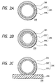
- Figs. 2A, 2B and 2C are schematic cross-sectional views illustrating composition of a collector electrode having a plurality of coating layers and the fixation condition of the collector electrode on to a substrate.
- Fig. 3 is a schematic cross-sectional view illustrating for a wire coat device used for manufacturing a collector electrode of the present invention.
- Fig. 5 is a schematic cross-sectional view illustrating composition of a solar cell of single crystal silicon type, according to the present invention.
- Fig. 6 is a schematic cross-sectional view illustrating composition of a solar cell of polycrystal silicon type, according to the present invention.
- Fig. 7 is a schematic cross-sectional view illustrating composition of a thin film solar cell of polycrystal silicon type according to the present invention.
- Figs. 8A and 8B are schematic plan views illustrating composition of a solar cell that is an example of the photovoltaic element according to the present invention.
- Fig. 9 is a schematic cross-sectional view illustrating composition of a photovoltaic elements module using a collector electrode having two layers coating, according to the present invention.
- Fig. 10 is a schematic cross-sectional view illustrating composition of a photovoltaic elements module using a collector electrode having two or three layers coating, according to the present invention.
- Fig. 11 is a schematic cross-sectional view illustrating composition of a photovoltaic elements module using a collector electrode having three layers coating, according to the present invention.
- Fig. 12 is a graph showing the relationship between volume resistivity and conversion efficiency in a module of photovoltaic elements according to the present invention.
- Fig. 13 is a schematic plan view illustrating composition of another module of photovoltaic elements using a collector electrode having the coating layer, according to the present invention.
- Fig. 14 is a graph showing the relationship between steaming cycles and series resistance for a module of photovoltaic elements according to the present invention.
- the problem arising in the formation of the existing collecting electrode, during the process following the coating and drying of the wire; in environments where light and moisture are present; was found to be caused by electromotive force being applied to the collecting electrode, thereby diffusing ions from the metal wire to the conductive resin layer.
- the problem of shunt with the existing collecting electrode formation was found to be caused by the possibility that the metalwire could contact the semiconductor layer or the transparentconductive film, because the conductive resin coating consisted of only one layer.
- Enamel wires, etc. are made by coating these metal wires with insulating varnish, but generally, it is not easy to coat metal, which are inorganic, with material that contains organic material.
- sufficient adhesive strength may not be obtained when adhering the wire, through the coating layer, to semiconductors and metals. This is because a special bond does no exist between the organic material in the coating layer and the semiconductor or metal material. This problem becomes even more pronounced depending on the metal material and its surface conditions, and we have discovered that almost no adhesive strength can be obtained when they are affected by moisture.
- the surface of the metal was altered in such a way that it will readily adhere to organic material, whereby a good adhesion between the metal and the conductive resin layer containing organic material was achieved based on the knowledge of this invention.
- Collecting electrodes are described in Figs. 1A and 1B, and 2A to 2C.
- the collecting electrode 100 shown in Fig. 1A is one in which the metal wire 101 is coated with one type of coating layer 102.
- the collecting electrode 200 shown in Fig. 2A is one in which the metal wire 201 is coated with two types of coating layers, namely, first coating layer 202 and second coating layer 203.
- the metal wires 101 and 202 composing the collecting electrode 100 and 200 are wire material, for which an industrially stable supply is available. It is also desirable that the material of the metal composing the metal wires 101 and 201, possess a resistivity of 10 ⁇ 4 ⁇ cm or less. For example, copper, silver, gold, platinum, aluminum, molybdenum and tungsten are suitable for use because of their low electric resistance. Of these, copper, silver and gold are the most desirable for their low electric resistance.
- the metal wire can also be an alloy of these metals.
- thin metal layers 103 and 204 such as those shown in Figs. 1B and 2B, on the surface of the metal wire; for purposes such as corrosion prevention, oxidation prevention, improvement of adhesion with the conductive resin and the improvement of electric conductivity.
- Candidates for metal layers to be applied to the metal wire surface are precious metals that offer resistance to corrosion, such as silver, palladium, silver and palladium alloy and gold, as well as metals with good corrosion resistance, such as nickel and tin. Of these, gold, silver and tin are not readily affected by moisture, therefore making them suitable for the metal layer.
- plating and cladding are suitable methods of forming the metal layer on the metal wire surface.
- the thickness of the coating will depend on individual preferences, the ideal thickness for metal wires with a circular cross section would be 1% to 10% of its diameter.
- the ideal resistivity of the metal layer considering the electric conductivity, effectiveness of corrosion resistance and the thickness of the metal layer, would be 10 ⁇ 6 ⁇ cm to 100 ⁇ cm.
- the cross section of the metal wire can be circular or rectangular and can be chosen depending on preferences.
- the diameter of the metal wire was designed so that the sum of the electric resistance loss and shadow loss is minimal.
- a copper wire for enamel wire with a diameter of 25 ⁇ m to 1mm, as indicated in the JIS-C-3203 is suitable for use. It is even more desirable to use diameters of 25 ⁇ m to 200 ⁇ m to create photovoltaic elements with good photoelectric exchange efficiency. Wires with diameters smaller than 25 ⁇ m are prone to breakage, difficult to produce and their power loss is larger. Meanwhile, diameters of 200 ⁇ m or more possess larger shadow loss or the surface of the photovoltaic element becomes bumpy, making it necessary to make the filler used on the surface coating layer, such as EVA, thicker.
- the metal wire is produced by using a well-known wire drawing machine to mold it into the desired diameter.
- the wire which has passed through the wire drawing machine is hard, but it will be annealed using a well-known method to meet desired characteristics in stretchability and bendability, and it can be also used as a soft wire.
- FIG. 1A An example of "a collecting electrode coated with a conductive adhesive consisting of one layer" according to this invention is shown in Fig. 1A.
- 101 is a metal wire for the electrode and 102 is the coating layer.
- the metal wire 101 is the core wire of the collecting electrode, and uses a wire that possesses good conductivity, such as copper wire, silver plated copper wire or silver copper clad wire, in order to reduce power loss.
- the coating layer 102 is formed from heat curing conductive adhesive or thermoplastic conductive adhesive, and its function is to mechanically and electrically connect the main part of the collecting electrode to the photovoltaic element substrate, through the thermocompression bonding process.
- FIG. 2A An example of "a collecting electrode coated with a conductive adhesive consisting of two layers" is shown in Fig. 2A.
- 201 is a metal wire for the electrode
- 202 is the first coating layer
- 202 is the second coating layer.
- the metal wire 201 is the core wire of the collecting electrode, and uses a wire that offers good conductivity, such as copper wire, silver plated copper wire or silver copper clad wire, in order to reduce power loss.
- the first layer 202 is formed with heat curing conductive adhesive, and protects the electrode metal, and provides mechanical and electrical connection. It also has the function of preventing migration by the electrode metal and controlling the flow of current into defective areas of the photovoltaic element from the collecting electrode.
- the second layer 203 is also formed of heat curing conductive adhesive, and its function is to mechanically and electrically connect the main part of the collecting electrode to the photovoltaic element substrate, through the thermocompression bonding process. And also because it heat cures, it is not readily damaged by paints used in the moisture prevention layer in later processes.
- the first coating layer 202 which is in direct contact with the metal wire 201, is a barrier layer which prevents moisture from reaching the metal wire to prevent corrosion of the metal wire surface, as well as prevent metal ion migration from the metal wire.
- the second layer 203 is an adhesive layer, which has the functions of adhering the collecting electrode to the semiconductor layer or transparent electrode and of current collection.
- the conductive adhesive that make up the first layer 202 resins with relatively little permeability are suitable for use among the resins mentioned above.
- urethane, epoxy, phenol or heat curing resins created by denaturating these resins are ideal.
- the thickness of the first layer be 1 ⁇ m to 15 ⁇ m, in order to prevent excessive shadow loss. Thicknesses of under 1 ⁇ m will make it difficult to create a uniform coating and pin-holes will occur, rendering it insufficient as a barrier.
- thicknesses of over 15 ⁇ m are not desirable because they are difficult to peel and shadow loss becomes too great.
- resins included in the conductive adhesive that make up the second layer 203 resins with good adhesive properties and good flexibility, in particular are suitable.
- urethane, epoxy, phenol or heat curing resins made by denaturating these resins or thermoplastic resins, such as phenoxy, polyamide or polyamideimide would be suitable.
- urethane resin is suitable for use because its bridging density is readily adjusted. It is desirable to leave these resins uncured after coating and cured only after the adhesion process is complete. For this reason, block isocyanate is desirable as the polymeric curing agent. This block isocyanate has the mechanism of progressively curing when heated above the dissociation temperature.
- any solvent contained in it can be completely removed, therefore depriving it of its stickiness and tackiness, allowing it to be coiled on a reel for storage.
- curing will not progress unless temperatures exceeding the dissociation temperature of the isocyanate are applied, it will uniformly provide sufficient adhesive strength during the formation of the collecting electrode.
- the thickness of the second coating layer will depend on the diameter of the wire. For example, if the diameter of the metal wire is 100 ⁇ m, the ideal thickness of the second coating layer would be 5 ⁇ m to 30 ⁇ m; which is a thickness that would have no pin-holes, would provide sufficient properties as an adhesive layer and offer no extreme shadow loss.
- FIG. 11 An example of "a collecting electrode coated with a conductive adhesive consisting of three layers" according to this invention is shown in Fig. 11.
- 1101 is the metal wire for the electrode
- 1102 is the first coating layer
- 1103 is the second coating layer
- 1104 is the third coating layer.
- the metal wire 1101 is the core wire of the collecting electrode, and uses a wire that offers good conductivity, such as copper wire, silver plated copper wire or silver copper clad wire, in order to reduce power loss.
- the first layer 1102 is formed of heat curing conductive adhesive, and provides electrical connection with the electrode metal.
- Metallic conductive adhesives would be suitable for the first coating layer 1102, to provide an electrical connection with the electrode metal.
- the second layer 1103 prevents migration caused by the metal fillers in the metallic conductive adhesive used in the electrode metal and the first coating layer. It also controls the flow of current to defective areas in the photovoltaic element from the collecting electrode.
- the third coating layer 1104 is also formed of heat curing conductive adhesive and its function is to mechanically and electrically connect the main part of the collecting electrode to the photovoltaic element substrate, through the thermocompression bonding process. And also because it heat cures, it is not readily damaged by paints used in the moisture prevention layer in later processes.
- the conductive adhesive used to coat the metal wire is made by distributing conductive particles and polymer.
- the resistivity of the conductive adhesive must be negligible in terms of collecting the electric current generated by the photovoltaic element and at the same time, provide adequate resistance to prevent shunt. In specific terms, 0.1 ⁇ cm to 100 ⁇ cm is desirable. When resistance is smaller than 0.1 ⁇ cm, the shunt retention function becomes insufficient and when it is greater than 100 ⁇ cm, loss from electric resistance becomes too great.
- Conductive particles according to this invention are pigment which add conductivity.
- Materials suitable for this purpose are, for example, carbon black, graphite, In2O3, TiO2, SnO2, ITO, ZnO and oxide semiconductor material made by adding the appropriate dopant to the material.
- the diameter of the conductive particles should be smaller than the coating layer to be formed, but if particles are too small the resistance on the contact point of the particles to each other becomes great and making it impossible to obtain the desired resistivity. For these reasons, the suitable average diameter for the conductive particles is 0.02 ⁇ m to 15 ⁇ m. It is also acceptable to adjust the resistivity and the distribution in the conductive resin by mixing two or more types of conductive particles. It is also acceptable to add translucency by using materials, such as ITO, In2O3, TiO2, SnO2 and ZnO. The usage of ITO produces especially good translucency.
- the conductive particles and the resin are mixed in suitable ratios to obtain the desired resistivity. Resistivity will decrease as the amount of conductive particles increase, but the coating layer will loose its stability as the proportion of resin decreases. And when the polymers are increased, the contact of the conductive particles to each other becomes faulty and will result in high resistance. Therefore, the optimum ratio should be determined depending on the polymer and conductive resin used, as well as its desired physical properties. In specific terms, good resistivity is obtained at volume percentages of the conductive particles ranging from 5% to 95%.
- the suitable resin according to this invention will be one that facilitates coat formation on the metal wire, with good workability, flexibility and weather resistance. Polymers with such characteristics are heat curing resins and thermoplastic resins.
- urethane, epoxy, phenol, polyvinyl formal, alkyd resin and resins made by denaturing these materials are examples which are suitable for use.
- urethane, epoxy and phenol resins are used as coating material for enamel lines, and are good in terms of flexibility and productivity. They are also suitable as material for collecting electrodes of the photovoltaic element, in terms of weather resistance and adhesion.
- thermoplastic resins butyral, phenoxy, polyamide, polyamideimide, melamine, butyral, acryl, styrene, polyester and fluoride are examples of suitable materials.
- butyral, phenoxy, polyamide and polyamideimide resins are good materials in terms of flexibility, weather resistance and adhesion, making them suitable for use in collecting electrodes of photovoltaic elements.
- a conductive adhesive consisting of a polymer containing a coupling agent and conductive particles are suitable. The reason why good characteristics are obtained when a conductive adhesion added with a coupling agent is used is described below.
- low resistance copper and aluminum wires used in wiring for electric appliances are inexpensive and good conductors.
- Enamel wires, etc. are made by coating these metal wires with insulating varnish, but generally, it is not easy to coat metal, which are inorganic, with material that contain organic material.
- sufficient adhesive strength may not be obtained when adhering (the wire), through the coating layer, to semiconductors and metals. This is because a special bond does not exist between the organic material in the coating layer and the semiconductor or metal material. This problem becomes even more pronounced depending on the metal material and its surface conditions, and we have discovered that almost no adhesive strength can be obtained when they are affected by moisture.
- the collecting electrode stated in this invention When the collecting electrode stated in this invention is used for solar batteries, its coupling agent acts to strengthen the bond between the organic material in the coating layer, with inorganic material, such as the surface of the solar cell substrate or metal tabs of the takeoff electrode. This makes it possible to prevent areas from loosing sufficient adhesive strength.
- the coating layer consists of two or more layers, effectiveness can be improved by determining the type of coupling agents to be used in the inner most side, which is in direct contact with the metal wire, and the outer most layer, which is in direct contact with the solar cell substrate; depending on the material of the metal wire, material of the solar cell substrate, material of the metal tab and the polymer composing these coating layers.
- the adhesive strength enhanced by the coupling agents is maintained in high temperatures, high humidity and high temperature/humidity environments, and therefore maintained even when the solar cell is used outdoors. This makes it possible to prevent deterioration of the exchange efficiency caused by the rise in series resistance from the deterioration of adhesive strength between the electrode and the solar cell substrate or metal tab, as well as from peeling.
- silane derivative coupling agent titanate derivative coupling agent and aluminum derivative coupling agent are among those cited.
- Such a coupling agent consists of a hydrophilic portion which has a mutual function with inorganic material and an organic function group which has a mutual function with organic material.
- the surface control between foreign materials is the main purpose of the use, particularly its function is based on a covalent bond and in this respect it is different from conventional surface active agents. That is, the coupling agent acts as go-between between a combination of inorganic material (metal) and an organic material (polymer in conductive adhesive) and the two materials are firmly combined.
- a silane derivative coupling agent is covalently bonded to both the inorganic material and the organic one, however, titanate derivative coupling agent and aluminum derivative coupling sometimes do not form covalent bonds of organic material.
- titanate derivative coupling agent and aluminum derivative coupling sometimes do not form covalent bonds of organic material.
- silane coupling agents suitable for this invention the following products are among those cited: ⁇ -mercaptoxy propyltrimethoxysilane, ⁇ -glycixidpropyltrimethoxysilane, ⁇ -(2-aminoethyl) aminopropyltrimethoxysilane, ⁇ -(2-aminoethyl) aminopropylmethyldimethoxysilane, aminosilane, ⁇ -anilinopropyltrimethoxysilane, vinyltriacetoxysilane, hexamethyldisilane, ⁇ -chloropropyltrimethoxysilane.
- titanate coupling agents suitable for the invention the following products are cited: isopropyltriisostearoyltitanate, tetra(2, 2-diallyloxymethyl-1-butyl) bis (di-tridecyl) phosphitetitanate, tetraisopyruvis (dioctylphosphite) titanate, isopropyltri (N-aminoethyl-aminoethyl) titanate, tetraoctyl bis (ditridecylphosphite) titanate, isopropyltris (dioctylpyrophosphanate) titanate, bis (octylpyrophosphate) oxyacetatetitanate.
- acetoalkoxyaluminiumdiisopropylate is cited.
- a coupling agent is mixed with a desirable solvent, adjusted and used.
- solvents are methanol, ethanol, isopropyl alcohol, toluene, benzene, acetone, methyl cellosolve, tetrahydrofuran and water.
- the solvent which is compatible with each coupling agent is selected and used. If solvent is used at high concentration, the activity of coupling agent would loose. Therefore, low concentration is used, 0.01% - 10.0% is usually optimum.
- the hydrophilic portion of the preceding coupling agent depends on silane, titanate, and aluminum derivatives; the suitability to the reaction of inorganic material must be considered.
- the organic function group of coupling agents are amino, epoxy, carboxy, phosphite radicals, etc. The suitability to reaction of organic material with these organic function groups must be considered.
- the polymer of more than 500 and less than 50,000 figure mean molecular mean weight is desirable.
- the dispersibility between the used polymer and the conductive particles in order to form a dense coating film, it is necessary to improve the dispersibility between the used polymer and the conductive particles, and to decrease the hole volume of the formed coating layer. It becomes possible to control the effect of humidity by proper selection and combination of polymers having more than 500 and less than 50,000 mean molecular weight and various kinds and diameters of conductive particles.
- the favorable resins for use are urethane, phenoxy, epoxy, butyral, phenol, polyimide, melamine, alkyd, fluorine polyvinylformal, polyamide, polyamideimide, polyester, acrylic and styrene resins.
- urethane, phenoxy, epoxy and phenol resins are widely used industrially for insulation material for enamel wire. Good properties in respect to humidity resistance, control of flexibility and productivity can be obtained.
- butyral resin has good dispersibility
- polyimide resin has good heat resistance.
- One way to measure the degree of bridging of the polymer is to measure its gel ratio.
- solvents such as xylene
- the gel parts that have bridged by gelation will not elute, but the sol parts which have not bridged will.
- bridging is complete, there will be no elution of the sol parts.
- the undissolved gel part, from which the sol part has been removed will remain.
- the gel ratio is obtained by measuring the amount of unbridged and eluted zol. The method of calculation is described below.
- Gel ratio [(weight of undissolved part) / original weight of specimen] ⁇ 100 (%) High gel ratios after the drying process will result in decreased adhesive strength during the formation of the collecting electrode. In addition, low sol ratios of the conductive resin layer of the collecting electrode formed by thermocompression, may result in decreased dependability when subjected to moisture.
- the mixing of the conductive particles and the polymer is conducted at a suitable ratio to obtain the desired resistivity. Resistivity will decrease as the amount of conductive particles increase, but the coating layer will loose its stability as the proportion of resin decreases. And when the polymers are increased, the contact of the conductive particles to each other becomes faulty and resulting in high resistance. Therefore, the optimum ratio should be determined depending on the polymer and conductive resin to be used, as well as its desired physical properties. In specific terms, good resistivity is obtained at volume percentages of the conductive particles ranging from 5% to 95%.
- the distributing devices used in "the mixing of the conductive particles and the polymer" according to this invention are, for example, regular triple roll mills, ball mills, paint shakers and bead mills. It is acceptable to add distributing agents and coupling agents as desired to improve distribution. It is also acceptable to dilute it with a suitable solvent to adjust the viscosity of the conductive adhesive, during or after distribution.
- Layer closer to the electrode are those layers which have either one or both of the following functions: to protect the metal wire used in the electrode from the surrounding environment or to establish an electrical connection with the metal wire.
- the resistivity of "layer closer to the electrode” must be such that it does not offer electric resistance when collecting the current generated by the photovoltaic element and a suitable range would be 0.1 ⁇ cm to 100 ⁇ cm.
- the contact layer of which the main ingredient is metal, as the "layer closer to the electrode".
- the contact layer has the function of improving the electrical contact between the metal wire and the conductive adhesive.
- Candidates materials for the contact layer are precious metals that offer resistance to corrosion, such as silver, palladium, silver and palladium alloy and gold, as well as metals with good corrosion resistance, such as nickel and tin.
- this consists of a conductive adhesive, it is desirable to produce an adhesive with the metal as its filler. It is also acceptable to form a layer of tin or silver on the metal wire by plating, without using conductive adhesives. Silver clad copper wires are also acceptable.
- metal based conductive adhesive When metal based conductive adhesive is used in the "layer closer to the electrode", it is acceptable to form a barrier layer on top of it that will prevent metal ion migration.
- the thickness of the barrier layer will vary depending on the wire diameter and preference. For example, for a wire with a diameter of 100 ⁇ m, a thickness of 1 ⁇ m to 15 ⁇ m would be desirable, to prevent pin-holes, to provide sufficient function as a barrier and to prevent excessive shadow loss. Thicknesses of under 1 ⁇ m make it difficult to create a uniform coating and pin-holes will occur, rendering it insufficient as a barrier. On the other hand, thicknesses of over 15 ⁇ m are not desirable because they are difficult to peel and shadow loss becomes too great.
- the void ratio of the conductive adhesive used in the barrier layer must be 0.04 ml/g or smaller, for a void radius of 1 ⁇ m or smaller.
- the glass transition point of the conductive adhesive after curing is 100 °C or higher. This will give it characteristics to sufficiently withstand the heat history during over-coating after the formation of the coating, as well as during the top coat agent and lamination processes.
- the conductive adhesive will be diluted to an appropriate viscosity, after which it will be coated onto the metal wire using a roll coater etc., after which it will be passed through dies or felt to form the desired thickness and finally dried and cured using infrared heating, etc.
- Fig. 3 is a type diagram describing a suitable coating device.
- 301 is the delivery reel
- 302 is the metal wire
- 303 is the cleaning tank
- 304 is the coater
- 305 is the die
- 306 is the drying oven
- 307 is the film thickness gauge
- 308 is the tension controller
- 309 is the aligned winding motor
- 310 is the take-up reel
- 311 is the temperature regulator.
- the delivery reel 301 is the bobbin to which the metal wire before coat formation is wound.
- the cleaning tank 303 is used only when required. This tank is filled with solvents, such as acetone, MEK and IPA, and is used to clean the surface of the metal wire 302 of any dirt.
- the coater 304 is a device which is used to apply the conductive adhesive to metal wire 302.
- the coater 304 contains a certain amount of conductive adhesive to be applied and can be equipped with a solvent adding mechanism for adjusting viscosity, a conductive adhesive replenishing mechanism or a filter mechanism if desired.
- the die 305 is a device which controls the thickness of the applied conductive adhesive to the desired thickness.
- the die 305 commercially available die for enamel coats are suitable for use, but felt may be used if desired.
- the drying oven 306 is used to remove solvent from the applied conductive adhesive and to dry it. It is also used for curing and if desired, these can be hot air driers or infrared driers.
- the film thickness gauge 307 is used to measure and manage the thickness of the applied conductive adhesive, and a commercially available outer diameter gauge is suitable for this purpose. It is also acceptable to use the information obtained through the film thickness gauge to conduct feedback controls, such as for delivery speed and viscosity of the conductive adhesive.
- the tension controller 308 maintains a constant tension, to prevent sag or forces exceeding the yielding point to be applied to the metal wire 302.
- the aligned winding motor 309 is a device that controls the spacing of the wire while the wire is being wound to the take-up reel 310.
- the take-up reel 310 is rotated at the desired speed, by a motor which is not shown in the figure.
- the temperature regulator is a device which maintains the temperature in the drying oven 306 at the set value. Well-known methods, such as slidack, on/off control and PID can be used if desired.
- Fig. 3 shows a vertically oriented device, but the direction of travel of the metal wire 302 can be either vertical or horizontal and can be determined based on preference.
- the wire When applying multiple coats of conductive adhesive, (the wire) may be taken up by the bobbin after each coating, but it may also be taken up by the bobbin after multiple coatings are complete.
- Fig. 3 shows the coating of one wire, but multiple wires may be coated simultaneously.
- the metal wire, onto which conductive adhesive has been coated, is to be stored wound to the bobbin, to be unwound for use when forming the collecting electrode for the photovoltaic element.
- Solar batteries configured as shown in Figs. 4A to 4C through Figs. 8A and 8B are examples of photovoltaic elements according to this invention.
- Figs. 4A to 4C Shown in Figs. 4A to 4C is a typical cross section of an amorphous silicone based solar cell, which receives light from the surface opposite the substrate.
- 401 is the substrate
- 402 is the lower electrode
- 403, 413 and 423 are the n-type semiconductor layers
- 404, 414 and 424 are i-type semiconductor layers
- 405, 415 and 425 are p-type semiconductor layers
- 406 is the upper electrode consisting of a transparent conductive film
- 407 is the grid electrode where a collector electrode is used.
- Fig. 5 shows a cross section of a monocrystal silicone solar cell.
- 501 is the semiconductor layer consisting of the silicone wafer substrate
- 502 is the semiconductor layer which forms a pn junction with the semiconductor layer 501
- 503 is the rear face electrode
- 504 is the collecting electrode
- 505 is the low reflection coating.
- Fig. 6 shows the cross section of a polycrystalline silicone solar cell
- 601 is a semiconductor layer consisting of a silicon wafer substrate
- 602 is a semiconductor layer which forms a pn junction with semiconductor layer 601
- 603 is the rear face electrode
- 604 is the collecting electrode
- 605 is the low reflection coating.
- Fig. 7 shows the cross section of a thin film polycrystalline silicon solar cell
- 701 is the substrate
- 702 is the polycrystalized semiconductor layer
- 703 is the semiconductor layer which forms a pn junction with semiconductor layer 702
- 704 is the rear face electrode
- 705 is the collecting electrode
- 706 is the low reflection coating.
- Figs. 8A and 8B show the solar cells shown in Figs. 4A to 4C through 7, from the light entry side.
- 801 is the substrate
- 802 is the positive electrode
- 803 is the negative electrode
- 804 is the collecting electrode.
- the structure of the "photovoltaic element" in this invention is desirable to consist of, for example, a semiconductor layer which contributes to electricity generation, a transparent conductive layer installed on the light entry side of the semiconductor layer, a collecting electrode consisting of the metal wire and conductive adhesive on the transparent electrode and a rear face electrode installed on the side opposite of light entry of the semiconductor layer.
- the semiconductor layer is required to have a structure which possesses semiconductor junctions, such as pn junction, pin junction or Schottky splicing, etc.
- Materials suitable for this purpose are, for example, semiconductors in the group IV, such as crystalline silicon, polycrystalline silicone and amorphous silicon, semiconductors in the group II-VI, such as Cds and CdTe, or semiconductors in the group III-V, such as GaAs.
- the collecting electrode is positioned on the light entry side of the semiconductor layer, positioned in a parallel configuration, with appropriate spacing.
- the electrode in this invention is particularly suitable for the formation of photovoltaic elements with large areas.
- collecting electrodes can be formed by placing electrodes, consisting of metal wires 30 cm in length and conductive adhesive, on the semiconductor layer at specified intervals.
- a bus bar electrode of relatively large capacity is to be formed.
- the rear face electrode of the photovoltaic element stated in this invention is one that is installed on the rear face of the semiconductor layer, the metal of which is formed, for example, by screen printing or deposition.
- the type of metal used, should be chosen from one that offers good ohmic contact with the semiconductor.
- the semiconductor layer When the semiconductor layer is made of a thin film consisting of monocrystal semiconductors containing amorphous silicon, microcrystal silicon or polycrystalline silicon based substances, it will need a subsidiary substrate. Both insulative and conductive substrates may be used for the subsidiary substrate. Substrates of metals, such as stainless steel or aluminum are suitable for use and these also function as the rear face electrode. When insulative substrates, such as glass, polymer and ceramics, etc. are used, metals such as chrome, aluminum or silver are to be depositioned to create the rear face electrode.
- the lower electrode 402 is an electrode on one side to retrieve the power generated in the semiconductor layers 403, 404, 405, 413, 414, 415, 423, 424 and 425, and is required to possess a work function that will create an ohmic contact with semiconductor layer 403.
- Materials used are, for example, metals or alloys, and transparent conductive oxides (TCO), such as Al, Ag, Pt, Au, Ni, Ti, Mo, W, Fe, V, Cr, Cu, nichrome, SnO2, In2O3, ZnO or ITO, etc. It is desirable that the surface of the lower electrode is smooth, but it may be textured if it is a cause of irregular reflection of light. Also, if substrate 401 is conductive, there is no need for a lower electrode 402.
- the lower electrode may be formed with well-known methods, such as plating, depositioning or spattering.
- n-layer 403, i-layer 404 and p-layer 405 are single structure with n-layer 403, i-layer 404 and p-layer 405 as one set suitable for the amorphous silicone semiconductor layer, but so are double or triple structure consisting of two or three sets of pin or pn junctions.
- Materials such as a-Si, a-SiGe and a-Sic, or the so called group IV and group IV alloy-type amorphous semiconductors, are suitable in particular, for the semiconductor material used for the i-layers 404, 414 and 424.
- Methods such as depositioning, spattering, high-frequency plasma CVD, microplasma CVC, ECR, heat CVD, and LPCVD methods, for example, can be used for the film formation of the amorphous semiconductor layer if desired.
- Transparent conductive film 406 is required when the sheet resistance is high, such as is the case with amorphous silicone. And because it is positioned on the light entry side, it is required to be transparent. Materials such as SnO2, In2O3, ZnO, CdO, CdSNO4 and ITO, for example are suitable for the transparent conductive film 406.
- monocrystal silicone solar cell 500 and polycrystalline silicon solar cell 600 a subsidiary substrate is not installed and the monocrystal wafer 501 and polycrystalline wafer 601 act as the substrates.
- the monocrystal wafer 501 is made by cutting, etc. an Si ingot which is pulled up with the CZ method.
- the polycrystalline wafer 601 is formed by cutting an Si ingot obtained with the cast method or by obtaining a polycrystal in sheet form using the ribbon method.
- the vapor phase diffusion method using POC 13 the coat diffusion method using TiO2, SiO2 or P2O5, or the ion placing method which dopes it directly in ions is used to make semiconductor layers 502 and 602.
- the rear face electrodes 503 and 603 are made by forming metal films with deposition or spattering, or by screen printing of silver paste.
- the low reflection coating 504 and 604 are formed to prevent the loss of efficiency, caused by light reflecting off of the solar cell surface. Suitable materials are, for example, SiO2, Ta2O5 and Nb2O5.
- the thin film polycrystal 700 is formed by growing Si polycrystal thin film 702 on substrate 701 made of alumina or graphite, etc. And in some cases, a particle diameter enlargement process is conducted, after which this is used as a substrate once again, onto which the base layer is formed, on top of which the surface layer 703 is formed using the epitaxial growth process. Low cost substrates, such as metal Si may be used for substrate 701.
- the second electrode consisting of the collecting electrode of this invention is positioned on the light entry side of the semiconductor layer. It is desirable that they be positioned in appropriate intervals, so that the sum of the loss caused by the electric resistance of current collecting and shadow loss is minimam. For example, if sheet resistance is approximately 100 ohms/ ⁇ , the desired intervals of the collecting electrodes would be about 5 mm. Also, optimization by narrowing pitch for thin diameter wires and widening pitch for thicker diameter wires will offer optimum efficiency.
- the electrode in this invention is particularly suitable for the formation of solar cells with large areas.
- collecting electrodes can be formed by placing electrodes of this invention, on the semiconductor layer at specified intervals.
- a tab may be positioned as the collector.
- a solar cell produced in this manner is encapsulated using a well-known process, for better weather resistance and to maintain its mechanical strength, and is modularized for outdoor use.
- EVA ethylene vinyl acetate
- a fluoride resin is laminated as a surface protectant to improve moisture and scratch resistance.
- Suitable materials are for example, a polymer of tetrafluoroethylene (TFE), a copolymer (ETFE) of tetrafluoroethylene and ethylene, polyvinyl fluoride and polychloro fluoroethylene (CTFE), etc.
- Fig. 10 is a type diagram of a photovoltaic element module 100, using a "collecting electrode coated with conductive adhesive consisting of two layers (hereinafter abbreviated as: two-layer coated collecting electrode)" of this invention.
- 1001 is the photovoltaic element substrate
- 1002 is the positive electrode
- 1003 is the negative electrode
- 1004 is the two-layer coated collecting electrode of this invention.
- Photovoltaic element substrate 1001 is made by forming films of p, i and n semiconductor and transparent conductive layers on the stainless steel substrate, using the CVD or spattering process.
- the positive electrode 1002 is an electrode which is used to retrieve the current collected by the collecting electrode and materials suitable for this are, for example, copper or silver plated copper which offer good conductance.
- the negative electrode 1003 is an electrode which is used to retrieve current from the stainless steel substrate and the material suitable for this would also be copper.
- the two-layer coated collecting electrode 1004 has the function of collecting the current generated by the photovoltaic element substrate.
- the two-layer coated collecting electrode 1004 is mechanically and electrically connected to the photovoltaic element substrate and the positive electrode by means of the thermocompression process.
- the metal wire is positioned as the collecting electrode on the photovoltaic element; for example, when more than one wires are to be positioned on the surface of the photovoltaic element surface; optimum efficiency can be obtained with optimization procedures, namely narrowing the pitch for thin wires and widening the pitch for thicker wires.
- the outer most layer of the collecting electrode must not be cured during application on the wire and only be dried of the solvent. And heated when adhering to achieve adhesion and curing.
- One method of production of the photovoltaic element of this invention is, for example the production method of photovoltaic cells described below.
- the desirable heating temperature would be the softening point of the adhesive layer and the conductive resin of the second layer, which will form the adhesive layer. It is desirable that only the adhesive layer and the second layer will be softened to make the collecting electrode adhere to the solar cell, without softening the first layer to maintain the initial film thickness. Also, if block isocyanate is used as the curing agent for the conductive resin, it is desirable to apply temperatures exceeding the dissociation temperature of isocyanate, so that curing will occur during the adhesion process.
- the desirable pressure will be such that the adhesive layer and said second layer will undergo moderate deformation, but must also be lower than any pressure that will destroy the solar cell.
- 0.1kg to 1.0 kg/cm2 would be suitable for solar cells with thin films, such as amorphous silicon.
- the desirable adhesive method would be to soften them and adhering them to the solar cell. Suitable pressure may be applied during adhering. If the second layer is thermoplastic, it will soften with heat. For heat curing resins, it is acceptable to dry the solvent, leaving the resins uncured during the application process to the wire for them to be heat cured during adhesion.
- the collecting electrode of this invention and the photovoltaic elements using the collecting electrode and their production method are entirely applicable to the photovoltaic elements other than the solar cell.
- One of the problems of production is that, in order to produce coated wire electrodes off-line and to facilitate storage until the formation of electrodes, it is difficult to control accelerated hardening of the resins, after the resin has been coated and dried on the metal wire.
- block isocyanate as the curing agent, only the solvent contained in the resin is dried during and after the coating drying process, and by heating it at a constant temperature, the block agent dissociates, allowing active isocyanate radicals to react with the resin to achieve hardening.
- block isocyanate as the curing agent.
- Another production related problem was, that it is convenient for handling if the metal wires are wound to a bobbin, etc. after the resin has been coated, however, the tackiness of the coated wires themselves made it difficult to unwind them from the bobbin and in some cases where tackiness was strong, the coating would peel off. This occurs when the glass transition point of the coating layer resin is low. By using resins with glass transition points of over 0 °C, the effects of tackiness reduction can be felt, but better results are obtained when the glass transition temperature is over 100 °C. Also, by mixing polymers with different glass transition points, it becomes possible to form coating layers with superior properties in terms of flexibility, adhesion and reduced tackiness. Preferable combinations are urethane resin and phenoxy resin, etc.
- the dispersibility of conductive particles into resin becomes important as well as the selection of high polymer.
- the diameter of a conductive particle should be formed smaller than the thickness of conductive coating layer, too small diameter increases resistance at the surface of particles where they contact each other, making it impossible to obtain the desired resistivity.
- agglomerated particles exist; such as primary particles which are systematically agglomerated crystallites, secondary particles which consist of primary particles agglomerating with particles' surface charge or van der Waals force or with other force. If the dispersibility is poor, agglomerated particles of a high order would exist to cause not only ununiform film thickness but also unstable conductivity.
- This invention has solved the problem by making the average diameter of primary particles of conductive particles in the coating layer bigger than 0.02 ⁇ m and smaller than 15 ⁇ m, the sizes which prevent formation of agglomerated particles of a higher order.
- the method to measure particles' agglomerating state in dispersion and particles' diameter there are the laser diffraction method, the light-particle correlation method, the light scattering method etc.
- the suitable conductive particles for the coating layer are graphite, In2O3, SnO2, TiO2, ITO, ZnO, and oxide semiconductor materials made from the materials by adding suitable dopants.
- the conductive particles and the polymer are mixed at a suitable ratio to obtain the desired resistivity. Although increased conductive particles reduce resistivity, they decrease the ratio of resin resulting in poor stability as coating film. Therefore, a suitable ratio should be properly selected considering what kind of high polymer and conductive particles will be used and what physical property value is desired for the film. Going into detail, around 5 volume percent to 95 volume percent of conductive particles give good resistivity.
- ordinary dispersing methods such as a three-roll-mill or a paint shaker etc., can be used.
- the conductive paint can be diluted with a suitable solvent to adjust viscosity.
- a problem during and after the formation of electrodes on a photovoltaic element is forming of pinholes which causes leakage current to defective parts reducing the characteristics of the photovoltaic element.
- this problem is solved by forming coated layers precisely and forming coating layers with sufficient thickness.
- the thickness of the coating layer varies with the diameter of the metal wire or characteristics desired. For example, when the metal wire is 100 ⁇ m in diameter, to have sufficient function as a barrier layer against leakage current, at the same time not to cause extreme shadow loss, the suitable thickness is between 1 ⁇ m and 30 ⁇ m.
- Another problem is, while forming of electrodes, metal wires touch the solar cell substrate to cause shunt.
- the solution to this problem is to form more than 2 of coating layers, and to harden completely the innermost layer of the coating layer while coating. In this way, metal wires are prevented from direct contact with the solar cell substrate during the compression process.
- the problems, such as migration etc., which occur when a photovoltaic element is used outdoors, can be solved by separating functions into layers; by preparing more than 2 layers of coating layers to share the functions such as current collecting, shunt prevention, migration prevention, electrode fixing, etc.
- Fig. 2A shows the sectional plan of an electrode with conductive coating layer on.
- Fig. 2C shows the sectional plan of the part where the electrode is fixed on a photovoltaic element substrate through the coating layer.
- 201 is the metal wire
- 202 is the primary coating layer which is directly coated on the metal wire
- 203 is the secondary coating layer which forms the outermost layer
- 205 is the coating layer (the whole) composed of conductive adhesive
- 206 is the photovoltaic element substrate.
- Coating of conductive coating layers is desired to be made cocentrically.
- the ordinary spreading method of insulating coating film the method used for enameled wire, can be suitably used.
- the conductive resin is diluted with a solvent to obtain suitable viscosity, then coats the metal wire with a roll coater, etc.
- the coated wire is passed through the dice to form a desired thickness, and is put in a furnace for drying the solvent and heat curing.
- Fig. 4A shows an amorphous silicon solar cell which has single cell structure with the light incidence on the other side of the substrate.
- Fig. 4C shows an amorphous silicon solar cell which has a triple structure of the solar cell in Fig. 4A.
- Fig. 13 shows the solar cells when looked at from the side of light incoming side shown in Figs. 4A and 4C. Grid electrodes of about 30 cm long are seen formed.
- composition according to the invention's idea can be applied to amorphous silicon solar cells which are accumulated on a transparent insulated substrate, and also to monocrystalline and thin-film polycrystalline solar cells.
- 401 shows the subsidiary substrate
- 402 shows the lower electrode
- 403, 404, and 405 respectively show the semiconductor layer which form pin-junction
- 406 shows the upper electrode of transparent conductive film
- 407 shows the grid electrode using collecting electrode.
- Fig. 4C 403, 404, and 405 show the semiconductor layers which form the first pin-junction
- 413, 414, and 415 show the semiconductor layers which form the second pin-junction
- 423, 424, and 425 show the semiconductor layers which form the third pin-junction.
- Fig. 1301 shows the metal tab
- 1302 shows the output port of anode
- 1303 shows the output port of cathode.
- the substrate 401 according to the invention is a membrane which mechanically supports semiconductor layers 403, 404 and 405 which are a thin film solar cell such as non-crystaline silicone. It is also used as an electrode in some cases.
- the substrate 401 has a required heat resistance to the heat temperature for forming film of semiconductor layers 403, 404 and 405.
- electroconductive material such metals as Fe, Ni, Cr, Al, Mo, Au, Nb, Ta, V, Ti, Pt, Pb and Ti are used; these alloys, for example, brass and stainless steel thin plate and its complex, carbon sheet and zinc plated steel plate are among those that can be used.
- film or sheet of heat resistant resin such as polyester, polyethylene, polycarbonate, cellulose acetate, polypropylene, polyvinylchloride, polyvinylidenechloride, polystyrene, polyamide, polyimide and epoxy resin are used. Or the compound with the resin and glass fiber, carbon fiber, boron fiber, metal fiber are among those also cited. And on the surface of the thin metallic plate and resin sheet, a coating treatment with foreign material metal thin film and/or insulating thin film of SiO2, Si3N4, Al2O3, AlN, etc., is carried out by a sputtering, vapor deposition and plating method. Glass and ceramic are also cited.
- the lower electrode 402 is one electrode to take out the electric power generated at semiconductor layers 403, 404, and 405. It is required to have such a work function as to form an ohmic contact to the semiconductor layer 403.
- the semiconductor layer 403. for example, Al, Ag, Pt, Au, Ni, Ti, Mo, W, Fe, V, Cr, Cu, stainless steel, brass, nichrome, SnO2, In2O3, ZnO, ITO, etc. are used as simple metallic substances or as their alloys or as transparent conductive oxides (TCO), etc.
- TCO transparent conductive oxides
- the surface of the lower electrode 402 is desirable to be smooth, the surface can be textured to cause diffused reflection of light.
- the lower electrode 402 is not necessarily to be prepared.
- the methods to prepare the lower electrode are plating, deposition, spattering etc.
- the methods to prepare the upper electrode there are the ohmic-resistance heating deposition method, the electron beam heating deposition method, the spattering method, the spraying method etc. to choose the desired.
- the named semiconductor layers are amorphous silicon, polycrystalline silicon, monocrystalline silicon, etc.
- the semiconductor materials to compose i-layer 404 are; a-Si:H, a-Si:F, a-Si:H:F, a-SiGe:H, a-SiGe:F, a-SiGe:H:F, a-SiC:H, a-SiC:F, a-SiC:H:F, etc.
- the named are, what is called, IV group and the IV group's alloy-amorphous semiconductor.
- the semiconductor materials to compose p-layer 405 or n-layer 403 are obtained from the semiconductor materials for the i-layer 404 by doping valence electron control agent.
- the materials for valence electron control agent to obtain p-type semiconductor the compounds of elements in group III of the periodic table are used. Elements in group III are B, Al, Ga, and In.
- the compounds of elements in group V of the periodic table are used. The elements in group V are P, N, As, and Sb.
- the methods to form films of amorphous silicon semiconductor layers can be chosen whatever desired from the well known methods such as the deposition method, the spattering method, the RF plasma CVD method, the microwave plasma CVD method, the ECR method, the thermal CVD method, the LPCVD method, etc.
- the RF plasma CVD method is favorably used, in which the material gas is decomposed with RF plasma and accumulated on the substrate.
- the RF plasma CVD method has problems such as the low yield in the material gas decomposition (about 10 %) and the slow accumulating speed (about 0.1 nm/sec. to 1 nm/sec.).
- the microwave plasma CVD method is attracting attention as an improved method for these problems.
- the reactor to do the film formation well known devices, such as the Batch reactor or a continuous film formation device, etc., can be used whatever desired.
- the invented solar cell can also be used for, what is called, tandem cell or triple cell, in which more than two semiconductor splices are laminated in order to obtain better spectral sensitivity and higher voltage.
- the upper electrode 406 is the electrode to take out electromotive force generated at the semiconductor layers 403, 404, and 405. It makes the pair to the lower electrode 402.
- the upper electrode 406 is necessary for semiconductors with high sheet resistivity, such as amorphous silicon. Because crystalline solar cells have low sheet resistivity, they do not necessarily need the upper electrode.
- the upper electrode 406 is positioned on the light incoming side and it needs to be transparent, and it is also called the transparent electrode.
- the upper electrode 406 is desirable to have more than 85 % of transmissivity for effective absorption of light from the sun and daylight fluorescent lamps etc. into semiconductor layers.
- the upper electrode 406 is desirable to have a sheet resistivity value of less than 100 ⁇ / ⁇ to let the electric current generated with light flow horizontally to the semiconductor layers.
- Materials with these characteristics are the metal oxides of SnO2, In2O3, ZnO, CdO, CdSnO4, ITO, etc.
- the grid electrode 407 consists of the metal wire 201, as shown in Fig. 2A, and the conductive coating layer 205.
- the conductive coating layer 205 needs to have resistivity value which is low enough not to reduce the efficiency of photovoltaic element and at the same time high enough to prevent shunt. That is, it does not act as resistance to the electric current generated by solar cells, but works as resistance to prevent serious leakage when any defect is around.
- the suitable resistivity value for the conductive coating layer 205 depends on the design of the grid, and on the photovoltaic element's electric current value and the scale of defect at its operating point.
- the desirable resistivity value is 0.1 - 100 ⁇ cm.
- the grid electrode 407 is positioned on the light incoming surface side of the photovoltaic element 400 (shown in Fig. 4A). As the grid's arrangement, the parallel arrangement with suitable intervals is recommendable.
- the invented collecting electrodes are particularly suitable for forming a solar cell with large area. For example, when solar cell of 30 cm2 is built, all needed is to install the invented collecting electrodes of 30 cm long parallel on the semiconductor layer with prescribed intervals. Furthermore, because the electrode is composed to reduce the current leakage caused by shunt or leaks, it is suitable for amorphous silicon solar cells. However, such composition is, of course, applicable to other types of solar cells than amorphous silicon type; to the solar cell of monocrystalline, polycrystalline, or of other semiconductors than silicon, or of Shottky splicing type.
- the tab 501 is the collector which collects the flowing current at the grid electrode 407 to one end.
- the materials for the collector metals like Cu, Ag, Pt, and alloys of these metals are usable.
- the desirable shapes are sheets, tapes, or foils to be glued with adhesive agents.
- the method to form the collecting electrode on the photovoltaic element the following method is illustrated as how to build solar cells.
- the collecting electrodes are desirable to be glued on the light incoming side of the semiconductor layer or on the surface of the transparent conductive film, using heat, pressure, or both.
- the favorable heating temperature is to higher than the softening point of the outermost coating layer, which is to become the glueing layer, and of the high polymer which forms the coating layer.
- the conductive resin's hardening agent is composed of block isocyanates, it is desirable to keep the temperature higher than the block isocyanate's dissociation temperature, then let the resin cause heat curing while glueing process.
- the favorable pressure should be high enough to suitably transform the glueing layer, the outermost layer of the coating layer, but should be lower than the pressure which keeps the solar cell without damaging. Going into detail, for example, for a film-type solar cell, such as amorphous silicon, a pressure of 0.1 kg/cm2 to 1.0 kg/cm2 will be suitable.
- the glueing method when the glueing layer, the outermost layer of the coating layer, is hot-melt-type, it is desirable to be glued to the solar cell by softening with heat. While glueing, a suitable pressure can be applied.
- 4 fluoro ethylene copolymer TFE Du Pont TEFLON
- copolymer of 4 fluoroethylene and ethylene ETFE Du Pont TEFZEL
- polyvinyl fluoride Du Pont TEDLER
- polyvinyl fluoride Du Pont TEDLER
- polychlorofluoroethylene CTFEC Daikin Industries Neoflon are cited.
- Weather resistance can also be improved by adding well-known UV absorber.
- the method for encapsulation for example, it is desirable to use well known devices such as the vacuum laminater, for thermocompression bonding of the solar cell substrate and the resin film in a vacuum.
- a collecting electrode is composed of Cu wire, carbon black, and urethane.
- the collecting electrode 100 of this invention was formed as follows.
- the metal wire 101 copper wire of 100 ⁇ m in diameter was used.
- the carbon paste, to form conductive adhesive for the coating layer 102 was prepared as follows. First, a mixed solvent of ethyl acetate 2.5 g and IPA 2.5 g was placed in a shake bottle for dispersion. Next, 22.0 g of urethane resin, the main ingredient, was added into the shake bottle, and all was mixed thoroughly with the ball mill. The number average molecular weight of urethane resin was 3000. Then, 1.1 g of block isocyanate, as a hardening agent, and 10 g of glass beads, for dispersion, were added to the solution. Then, as conductive particles, 2.5 g of carbon black of 0.05 ⁇ m in average primary particle diameter was added to the solution.
- the shake bottle containing the materials was placed in a paint shaker, of Toyo Seiki Co., for 10 hours for dispersion. Then glass beads for dispersion were removed from the prepared paste. The average particle diameter of the paste was measured to be about 1 ⁇ m. The results of using the beads mill instead of a paint shaker were almost the same.
- the paste was hardened at 160°C for 30 minutes, the standard hardening condition of the hardening agent. Its volume resistivity was measured to be 0.6 ⁇ cm to prove being low enough.
- the void ratio of the paste was measured by a mercury Polosimeter to be 0.01 ml/g. Then, carbon black was removed from the paste and only resin was hardened to form a sheet. Its gel ratio was measured to be approximately 100 %.
- the coating layer 102 was formed as follows, using a vertical wire-coating machine 300 shown in Fig. 3.
- the delivery reel 301 was set with a reel which is wound with metal wire 307.
- the metal wire was stretched toward the take-up reel 310.
- the paste was poured into the coater.
- the coating speed was 40 m/min, and the residence time was 2 seconds.
- the drying furnace 306 was set at 120°C.
- the coating was done 5 times.
- the dice, the one for enamel coating, were used in a variety of diameters, from 110 ⁇ m to 200 ⁇ m in order. Under this condition, the paste was preserved, with solvent evaporated and in unhardened state.
- the thickness of the coating layer 102 was 20 ⁇ m on average. Variations in the film thickness after coating were within ⁇ 0.5 ⁇ m per 100 m.
- an amorphous solar cell 400 was built. It had the layer composition shown in Fig. 4C and pin-junction-type triple structure with grid electrodes of 30 cm long.
- an SUS 430 BA substrate 401 was thoroughly degreased and washed, then was placed in a DC spattering device (not illustrated) to accumulate 450 nm of Ag followed by 1000 nm of ZnO. Thus the lower electrode 402 was formed.
- the substrate was taken out and placed in a microwave plasma CVD film formation device (not illustrated) to form in order of silicon layer as the n-layer 403, silicon-germanium layer as the i-layer 404, and silicon layer as the p-layer 405.
- the bottom layer was formed.
- the middle layer was formed in order of silicon layer as the n-layer 413, silicon-germanium layer as the i-layer 414, and silicon layer as the p-layer 415.
- the top layer of the silicon layer was formed in order of the n-layer 423, the i-layer 424, and the p-layer.
- the semiconductor layer was accumulated.
- it was placed in the spattering device (not illustrated) to form 70 nm of ITO film, the transparent conductive film 406, which also has low reflectance function.
- the solar cell substrate 401 was trimmed into the size of 30 ⁇ 30 cm with an effective area of 900 cm2 by removing unnecessary part of transparent conductive film, using etching paste, whose main ingredient is ferric chloride, and a printer on the market.
- the anode 802 and the cathode 803, both of hard copper were prepared.
- the coated wire 100 was stretched between the both anode 802 at 6 mm intervals and to be within the effective area, then was fixed with an ultraviolet-ray hardening adhesive.
- the fixed said coating wire 100 was bonded by thermocompression, using a heating device (not illustrated), to form the collecting electrode 804 on the cell surface of the solar cell substrate 401 and on the anode 802.
- a heating device not illustrated
- the heating condition was; at 200°C, for 45 seconds, and at the pressure of 1 kg/cm2.
- the encapsulation of this sample was done as follows. On the top and bottom of the solar cell substrate 801, plane glass and EVA were laminated, and fluorine-contained resin film ETFE (Tefzel of Du Pont) was laminated further on the top and bottom of it. Then, the substrate was placed in a vacuum laminater and laminated at 150°C for 60 minutes.
- ETFE Tefzel of Du Pont
- the initial characteristics of the obtained sample were measured as follows. First, the voltage/current characteristics were measured in the dark state. The shunt resistivity was measured at the slope near the home position to be 200 k ⁇ cm2 to 500 k ⁇ cm2, favorable results. Next, the solar cell characteristics were measured, using pseudo solar light source (hereafter called simulator) with quantity of light of 100 mW/cm2 by the AM 1.5 global sunlight spectrum. The obtained conversion efficiency was 9.6 % + 0.02 %, showing favorable characteristics with little variations. The series resistivity was 32.0 ⁇ cm2 on average, also a favorable value. The yield rate of normal I-V curve was favorable 94 %.
- the reliability test was given to these samples in conformity with the Japanese Industrial Standards C 8917; the environmental testing method for crystalline solar cell modules, and the hygrothermal cycle test A - 2 provided by the endurance testing method.
- thermo-hygrostat which can control temperatures and humidity, and repeated 20 times of cycle tests varied between -40°C and +85°C (with relative humidity 85 %). Then, the samples, which completed the cycle test, were measured their solar cell characteristics in the same way as the initial characteristics were, using the simulator. Its conversion efficiency was lower 2 % on average than the initial value, showing no occurrence of meaningful deterioration.
- the collecting electrode consists of Cu wire with fluorine-contained resin paste containing carbon.
- the conventional collecting electrode 100 was built in the same way as in Embodiment 1, in Fig. 1A, with the following exceptions.
- the paste, used for the coating layer 102 of the collecting electrode 100 in Fig. 1A, was a fluorine-contained resin paste (Electrodag +502 SS of Acheson Colloid), similar to the one mentioned in the U. S. Patent No. 4,260,429.
- the wire was coated in the same way as in Embodiment 1.
- the thickness of the coating layer 102 was 20 ⁇ m on average, and the deflection of film thickness in 100 meter long was over ⁇ 1.0 ⁇ m after coating.
- the paste was hardened at 120°C for 5 minutes, the standard hardening condition for the hardening agent.
- the volume resistivity was measured to be 0.1 ⁇ cm2, a low enough value.
- the hole volume of this conductive adhesive was 0.05 ml/g. Then, like in Embodiment 1, 50 solar cell modules were built, using this wire as collection electrodes.
- the initial characteristics of the obtained sample were measured in the similar method to Embodiment 1.
- the shunt resistivity was measured to be 4 k ⁇ cm2 - 300 k ⁇ cm2, showing a wide variation.
- the conversion efficiency was obtained to be 9.0 % ⁇ 1.2 %, varying widely.
- the series resistivity of normal 1 - 1 V curve was obtained to be 32.1 ⁇ cm2 on average, a favorable value.
- the initial yield rate of normal I - V curve was as low as 64 %.
- the reliability test was done to this sample similarly to Embodiment 1.
- the tested sample was measured its solar cell characteristics with the simulator similarly to the initial characteristics. The result was on average 11 % lower than the initial conversion efficiency, showing the occurrence of meaningful deterioration.
- the series resistivity was measured to have risen to 62 ⁇ cm2 on average. This indicated that the rise of the series resistivity caused the deterioration of the conversion efficiency.
- the collecting electrode consists of Cu wire, ITO, and butyral.
- the above-described paste was hardened at the temperature of 160 °C for thirty minutes which were the standard hardening condition of the above-described hardener and then was measured in its volume resistivity, and it was verified that its volume resistivity was low enough because the measured value was 1.2 ⁇ cm2. Further, transmittance of light was measured using a spectroscope and its transmittance was satisfactory because the measured value was 90% per 400 nm.
- the volume of a hole of this conductive adhesive agent was 0.02 ml/g and the ratio of gel was 20%.
- the average molecular weight of polymeric resin was fifty thousand.
- Wire was coated as the first embodiment to form a collecting electrode 100.
- Fifty solar battery modules were produced using the collecting electrode 100 by the same method as that in the first embodiment.
- the initial characteristics of the obtained sample were measured by the same method as that in the first embodiment and satisfactory characteristics could be obtained because its conversion efficiency was 9.7% ⁇ 0.05%, its shunt resistance was 250 to 300 k ⁇ cm2, its series resistance was 32.5 ⁇ cm2 on average.
- the yield rate of samples of which I-V curve was normal was satisfactory because it was 94%.
- the reliability test of these samples was performed by the same method as that in the first embodiment. Next, the solar battery characteristics of the samples after the test was finished were measured using a simulator as in measurement of initial values, and its measured conversion efficiency was lower 2% on average than the initial conversion efficiency, however, no significant deterioration occurred.
- the result of this embodiment shows a solar battery using a collecting electrode according to the invention has excellent characteristics and high reliability.
- a collecting electrode comprises Ag wire, urethane and SnO2
- a collecting electrode 100 according to the invention shown in Fig. 1A is produced as the first embodiment except that a metallic wire 101 is formed by silver, and SnO2 powder manufactured by Mitsui Mining and Smelting Co., Ltd. of which average primary particle diameter is 0.2 ⁇ m is used as a conductive particle forming a coated layer 102.
- the above-described paste was hardened at the temperature of 160 °C for thirty minutes which were the standard hardening condition of the above-described hardener and then, was measured in its volume resistivity, and it was verified that its volume resistivity was low enough because the measured value was 1.0 ⁇ cm2.
- Wire was coated as the first embodiment to form a collecting electrode 100. Fifty solar battery modules were produced using the collecting electrode 100 by the same method as that in the first embodiment.
- the initial characteristics of the obtained sample were measured by the same method as that in the first embodiment and satisfactory characteristics could be obtained because its conversion efficiency was 9.1% ⁇ 0.06%, its shunt resistance was 250 to 400 k ⁇ cm2, its series resistance was 32.9 ⁇ cm2 on average.
- the yield rate of samples of which I-V curve was normal was satisfactory because it was 92%.
- the reliability test of these samples was performed by the same method as that in the first embodiment. Next, the solar battery characteristics of the samples after the test was finished were measured using a simulator as in measurement of initial values, and the conversion efficiency was lower 2.5% on average than the initial conversion efficiency, however, no significant deterioration occurred.
- the result of this embodiment shows a solar battery using a collecting electrode according to the invention has excellent characteristics and high reliability.
- a collecting electrode comprises Au wire, polyamide and In2O3 will be described.
- a collecting electrode 100 according to the invention shown in Fig. 1A is produced as the first embodiment except that a metallic wire 101 is formed by gold, polyamide resin manufactured by Mitsubishi Chemical Industries Ltd. is used as polymeric resin which mainly constitutes paste forming a coated layer 102, and In2O3 manufactured by Sumitomo Metal Mining Co., Ltd. of which average primary particle diameter is 0.05 ⁇ m is used as a conductive particle.
- the above-described paste was hardened at the temperature of 160 °C for thirty minutes which were the standard hardening condition of the above-described hardener and then, was measured in its volume resistivity, and it was verified that its volume resistivity was low enough because the measured value was 1.5 ⁇ cm2.
- the volume of a hole of this conductive adhesive was 0.04 l/g and average molecular weight of polymeric resin was ten thousand.
- Wire was coated as the first embodiment to form a collecting electrode 100.
- Fifty solar battery modules were produced using the collecting electrode 100 by the same method as that in the first embodiment.
- the initial characteristics of the obtained sample were measured by the same method as that in the first embodiment and satisfactory characteristics could be obtained because its conversion efficiency was 9.2% ⁇ 0.01%, its shunt resistance was 400 to 500 k ⁇ cm2, its series resistance was 32.3 ⁇ cm2 on average.
- the yield rate of samples of which I-V curve was normal was satisfactory because it was 90%.
- the reliability test of these samples was performed by the same method as that in the first embodiment. Next, the solar battery characteristics of the samples after the test was finished were measured using a simulator as in measurement of initial values, and the conversion efficiency was lower 2% on average than the initial conversion efficiency, however, no significant deterioration occurred.
- the result of this embodiment shows a solar battery using a collecting electrode according to the invention has excellent characteristics and high reliability.
- a collecting electrode comprises Cu wire, silver clad, urethane and carbon black.
- a collecting electrode 100 according to the invention shown in Fig. 1B is produced as the first embodiment except that a silver-clad copper wire 100 ⁇ m in diameter produced by forming a silver-clad metal layer 103 2 ⁇ m thick on a copper wire 101 to enhance adhesion and electrical connection with a conductive adhesive is used.
- Paste for forming a conductive adhesive for a coated layer 102 is produced as follows: First, mixed solution comprising ethyl acetate 2.5 g and IPA 2.5 g as a solvent is put in a shaker for dispersion. Next, urethane resin 22.0 g which is main material is added in the above-described shaker and is sufficiently stirred with a ball mill. Next, as a hardener, block isocyanate 1.1 g and glass beads for dispersion 10 g are added in the above-described solution. Next, carbon black 2.5 g of which average primary particle diameter is 0.05 ⁇ m as a conductive particle is added in the above-described solution.
- the shaker in which the above-described materials were put is dispersed with a paint shaker manufactured by Toyo Precision Mechanical Equipment for ten hours. Then, the glass beads for dispersion are removed from produced paste. The average particle diameter of the paste was measured and the measured value was approximately 1 ⁇ m. The similar result was also obtained if a bead mill was used in place of a paint shaker.
- the above-described paste was hardened at the temperature of 160 °C for thirty minutes which were the standard hardening condition of the above-described hardener and then, was measured in its volume resistivity, and it was verified that its volume resistivity was low enough because the measured value was 0.6 ⁇ cm2.
- a coated layer 403 is formed using a vertical-type wire coating machine 400 shown in Fig. 4 as described below.
- a layer 102 was coated on a silver-clad layer 103 as the first embodiment to form a collecting electrode 100.
- Fifty solar battery modules were produced using the collecting electrode 100 by the same method as that in the first embodiment.
- the initial characteristics of the obtained sample were measured by the same method as that in the first embodiment and satisfactory characteristics could be obtained because its conversion efficiency was 9.7% ⁇ 0.03%, its shunt resistance was 300 to 400 k ⁇ cm2, its series resistance was 31.5 ⁇ cm2 on average.
- the yield rate of samples of which I-V curve was normal was satisfactory because it was 90%.
- the reliability test of these samples was performed by the same method as that in the first embodiment. Next, the solar battery characteristics of the samples after the test was finished were measured using a simulator as in measurement of initial values, and the conversion efficiency was lower 1.5% on average than the initial conversion efficiency, however, no significant deterioration occurred.
- the result of this embodiment shows a solar battery using a collecting electrode according to the invention has excellent characteristics and high reliability.
- a collecting electrode comprises Cu wire, silver clad, phenoxy and ZnO will be described.
- a collecting electrode 100 according to the invention shown in Fig. 1B is produced as the fifth embodiment except that phenoxy resin manufactured by PKHH Tomoe Industries is used as polymeric resin which mainly constitutes paste forming a coated layer 102 and ZnO powder manufactured by Mitsui Mining and Smelting Co. Ltd. of which average primary particle diameter is 0.1 ⁇ m is used as a conductive particle.
- phenoxy resin manufactured by PKHH Tomoe Industries is used as polymeric resin which mainly constitutes paste forming a coated layer 102 and ZnO powder manufactured by Mitsui Mining and Smelting Co. Ltd. of which average primary particle diameter is 0.1 ⁇ m is used as a conductive particle.
- the above-described paste was hardened at the temperature of 160 °C for thirty minutes which were the standard hardening condition of the above-described hardener and then, was measured in its volume resistivity, and it was verified that its volume resistivity was low enough because the measured value was 1.3 ⁇ cm2.
- the volume of a hole of this conductive adhesive was 0.01 ml/g and the ratio of gel was 100%.
- the average molecular weight of polymeric resin was twenty-five thousand.
- Wire was coated as the fifth embodiment to form a collecting electrode 100.
- Fifty solar battery modules were produced using the collecting electrode 100 by the same method as that in the first embodiment.
- the initial characteristics of the obtained sample were measured by the same method as that in the first embodiment and satisfactory characteristics could be obtained because its conversion efficiency was 9.6% ⁇ 0.02%, its shunt resistance was 310 to 390 k ⁇ cm2, its series resistance was 32.4 ⁇ cm2 on average.
- the yield rate of samples of which I-V curve was normal was satisfactory because it was 94%.
- the reliability test of these samples was performed by the same method as that in the first embodiment. Next, the solar battery characteristics of the samples after the test was finished were measured using a simulator as in measurement of initial values, and the conversion efficiency was lower 2% on average than the initial conversion efficiency, however, no significant deterioration occurred.
- the result of this embodiment shows a solar battery using a collecting electrode according to the invention has excellent characteristics and high reliability.
- a collecting electrode 100 according to the invention shown in Fig. 1B is produced as the fifth embodiment except that ZnO powder produced by adding aluminum to ZnO as dopant so as to lower contact resistance of a conductive particle is used.
- the above-described paste was hardened at the temperature of 160 °C for thirty minutes which were the standard hardening condition of the above-described hardener and then, was measured in its volume resistivity, and it was verified that its volume resistivity was low enough because the measured value was 0.9 ⁇ cm2.
- Wire was coated as the fifth embodiment to form a collecting electrode 100.
- Fifty solar battery modules were produced using the collecting electrode 100 by the same method as that in the first embodiment.
- the initial characteristics of the obtained sample were measured by the same method as that in the first embodiment and satisfactory characteristics could be obtained because its conversion efficiency was 9.6% ⁇ 0.09%, its shunt resistance was 400 to 500 k ⁇ cm2, its series resistance was 31.5 ⁇ cm2 on average.
- the yield rate of samples of which I-V curve was normal was satisfactory because it was 92%.
- the reliability test of these samples was performed by the same method as that in the first embodiment. Next, the solar battery characteristics of the samples after the test was finished were measured using a simulator as in measurement of initial values, and the conversion efficiency was lower 2% on average than the initial conversion efficiency, however, no significant deterioration occurred.
- the result of this embodiment shows a solar battery using a collecting electrode according to the invention has excellent characteristics and high reliability.
- a collecting electrode comprises Cu wire, silver plating, urethane and TiO2 will be described.
- a collecting electrode 100 according to the invention shown in Fig. 1B is produced as the fifth embodiment except that a metallic layer 103 on a copper wire 101 is changed from silver clad according to the fifth embodiment to silver plating and TiO2 manufactured by Ishihara Sangyo Kaisha of which average primary particle diameter is 0.2 ⁇ m is used as a conductive particle.
- the above-described paste was hardened at the temperature of 160 °C for thirty minutes which were the standard hardening condition of the above-described hardener and then, was measured in its volume resistivity, and it was verified that its volume resistivity was low enough because the measured value was 1.1 ⁇ cm2. Wire was coated as the fifth embodiment to form a collecting electrode 100.
- Fifty solar battery modules were produced using the collecting electrode 100 by the same method as that in the first embodiment.
- the initial characteristics of the obtained sample were measured by the same method as that in the first embodiment and satisfactory characteristics could be obtained because its conversion efficiency was 9.5% ⁇ 0.01%, its shunt resistance was 400 to 500 k ⁇ cm2, its series resistance was 31.6 ⁇ cm2 on average. The yield rate of samples of which I-V curve was normal was satisfactory because it was 92%.
- the reliability test of these samples was performed by the same method as that in the first embodiment. Next, the solar battery characteristics of the samples after the test was finished were measured using a simulator as in measurement of initial values, and the conversion efficiency was lower 2.3% on average than the initial conversion efficiency, however, no significant deterioration occurred.
- the result of this embodiment shows a solar battery using a collecting electrode according to the invention has excellent characteristics and high reliability.
- a collecting electrode comprises Cu wire, tin plating, polyamide and graphite will be described.
- a collecting electrode 100 according to the invention shown in Fig. 1B is produced as the fifth embodiment except that a metallic layer 103 on a copper wire 101 is changed from silver clad according to the fifth embodiment to tin plating, and polyamide imide resin manufactured by Mitsubishi Chemical Industries Ltd. is used as polymeric resin which mainly constitutes paste and a conductive particle is changed to graphite manufactured by Tokai Carbon.
- the above-described paste was hardened at the temperature of 180 °C for thirty minutes which were the standard hardening condition of the above-described hardener and then, was measured in its volume resistivity, and it was verified that its volume resistivity was low enough because the measured value was 2.0 ⁇ cm2.
- the volume of a hole of this conductive adhesive was 0.01 ml/g and the average molecular weight of polymeric resin was twenty-five thousand.
- Wire was coated as the fifth embodiment to form a collecting electrode 100.
- Fifty solar battery modules were produced using the collecting electrode 100 by the same method as that in the first embodiment.
- the initial characteristics of the obtained sample were measured by the same method as that in the first embodiment and satisfactory characteristics could be obtained because its conversion efficiency was 9.3% ⁇ 0.09%, its shunt resistance was 400 to 500 k ⁇ cm2, its series resistance was 33.6 ⁇ cm2 on average.
- the yield rate of samples of which I-V curve was normal was satisfactory because it was 94%.
- the reliability test of these samples was performed by the same method as that in the first embodiment. Next, the solar battery characteristics of the samples after the test was finished were measured using a simulator as in measurement of initial values, and the conversion efficiency was lower 2.9% on average than the initial conversion efficiency, however, no significant deterioration occurred.
- the result of this embodiment shows a solar battery using a collecting electrode according to the invention has excellent characteristics and high reliability.
- a collecting electrode comprises Cu wire, silver paste, urethane and carbon black.
- a collecting electrode 100 according to the invention shown in Fig. 1B is produced as the fifth embodiment except that a metallic layer 103 on a copper wire 101 is changed from silver clad according to the fifth embodiment to silver paste, 5007 manufactured by Du Pont.
- paste in which a silver particle is dispersed in epoxy resin is used.
- the above-described paste was hardened at the temperature of 150 °C for thirty minutes which were the standard hardening condition of the above-described hardener and then, was measured in its volume resistivity, and it was verified that its volume resistivity was low enough because the measured value was 5 x 10 ⁇ 5 ⁇ cm2.
- a metallic layer 302 comprising the above-described silver paste which is coated on a Cu wire sequentially from the innermost layer by the same method as that in the first embodiment is constituted as follows: First, a reel on which a Cu wire 302 is wound is set on a delivery reel 301 and the above-described Cu wire is stretched to a take-up reel 310. Next, the above-described silver paste 5007 is injected into a coater.
- the take-up speed of Cu wire shall be 40 m/min., the hardening time 2 sec., the temperature of a drying furnace 200 °C and the diameter of the used die for enamel coating 160 ⁇ m.
- the above-described conditions on which paste 5007 applied on wire is hardened are determined based upon the result of experiments.
- the thickness of formed metallic layer 103 was 5 ⁇ m on average and fluctuation of the thickness of film when wire 100 m long was coated was within ⁇ 0.2 ⁇ m.
- a carbon paste-coated layer 102 comprising urethane resin was formed by the same method as that in the fifth embodiment.
- the thickness of the coated layer 102 was 20 ⁇ m on average and fluctuation of the thickness of film when a wire 100 m long was coated was within ⁇ 1 ⁇ m.
- the initial characteristics of the obtained sample were measured by the same method as that in the first embodiment. First, the shunt resistance was checked and a satisfactory value could be obtained because the measured value was 150 to 200 k ⁇ cm2. Next, the characteristics of the above-described solar battery were measured, and it was verified that such solar battery had satisfactory characteristics and such characteristics varied little because its conversion efficiency was 9.2% ⁇ 0.05% and its series resistance was 31.8 ⁇ cm2 on average. The yield rate of samples of which I-V curve was normal was satisfactory because it was 88%.
- the reliability test of these samples was performed by the same method as that in the first embodiment. Next, the solar battery characteristics of the samples after the test was finished were measured using a simulator as in measurement of initial values, and the conversion efficiency was lower 2.1% on average than the initial conversion efficiency, however, no significant deterioration occurred.
- the shunt resistance of such sample after the above-described test was finished was measured by the same method as that in the first embodiment, as a result, the measured value was 130 to 160 k ⁇ cm2, and no significant deterioration occurred.
- the result of this embodiment shows a solar battery using a metallic wire on which a conductive adhesive is coated according to the invention as a collecting electrode has excellent characteristics and high reliability.
- an amorphous solar battery 400 is produced according to the following procedure by the same method as that in the first embodiment except that it is constituted as a single type which is constituted only by a Si layer shown in Fig. 4A and radio-frequency (RF) plasma CVD is used for forming a semiconductor layer.
- RF radio-frequency
- SUS430BA substrate 401 sufficiently degreased and cleaned is put in a DC sputtering device not shown, Ag is deposited until the film is 400 nm thick, then ZnO is deposited until the film is 400 nm thick so as to form the lower electrode 402.
- the substrate is taken out of the sputtering device and is put in a RF plasma CVD film forming system not shown, and a silicon semiconductor layer is formed in the order of n layer 403, i-layer 404 and p-layer 405.
- the substrate is put in a resistance heating deposition system not shown and In2O3 film is formed as transparent conductive film 506 provided with a function also with anti-reflection effect.
- fifty solar battery modules were produced using the above-described collecting electrode 100 by the same method as that in the first embodiment. At this time, the above-described coated wire 100 was used at intervals of 5.5 mm.
- the initial characteristics of the obtained sample were measured by the same method as that in the first embodiment and satisfactory characteristics could be obtained because its conversion efficiency was 5.2% ⁇ 0.05%, its shunt resistance was 150 to 320 k ⁇ cm2, its series resistance was 9.5 ⁇ cm2 on average. The yield rate of samples of which I-V curve was normal was satisfactory because it was 90%.
- the reliability test of these samples was performed by the same method as that in the first embodiment. Next, the solar battery characteristics of the samples after the test was finished were measured using a simulator as in measurement of initial values, and the conversion efficiency was lower 2.4% on average than the initial conversion efficiency, however, no significant deterioration occurred.
- the result of this embodiment shows a solar battery using a collecting electrode according to the invention has excellent characteristics and high reliability.
- an amorphous solar battery 400 is produced according to the following procedure by the same method as that in the first embodiment except that it is constituted as a double type which is constituted by two Si layers shown in Fig. 4B and RF plasma CVD is used for forming a semiconductor layer.
- SUS430BA substrate 401 sufficiently degreased and cleaned is put in a DC sputtering device not shown, Ag is deposited until the film is 400 nm thick, then ZnO is deposited until the film is 400 nm thick so as to form the lower electrode 402.
- the substrate is taken out of the sputtering device and is put in a RF plasma CVD film forming system not shown, and the bottom layer of a silicon layer is formed in the order of n layer 403, i-layer 404 and p-layer 405.
- the top layer of a silicon layer is sequentially formed in the order of n layer 413, i-layer 414 and p-layer 415, and as a result, a silicon semiconductor layer is deposited.
- the substrate is put in a resistance heating deposition system not shown and In2O3 film is formed as transparent conductive film 406 provided with a function also with anti-reflection effect.
- the initial characteristics of the obtained sample were measured by the same method as that in the first embodiment and satisfactory characteristics could be obtained because its conversion efficiency was 7.5% ⁇ 0.01%, its shunt resistance was 400 to 500 k ⁇ cm2, its series resistance was 23.1 ⁇ cm2 on average.
- the yield rate of samples of which I-V curve was normal was satisfactory because it was 94%.
- the reliability test of these samples was performed by the same method as that in the first embodiment. Next, the solar battery characteristics of the samples after the test was finished were measured using a simulator as in measurement of initial values, and the conversion efficiency was lower 1.9% on average than the initial conversion efficiency, however, no significant deterioration occurred.
- the result of this embodiment shows a solar battery using a collecting electrode according to the invention has excellent characteristics and high reliability.
- an amorphous solar battery 400 is produced according to the following procedure by the same method as that in the first embodiment except that it is constituted as a double type which is constituted by Si and SiGe layers shown in Fig. 6, RF plasma CVD is used for forming a semiconductor layer, and a silicon germanium semiconductor layer is used for i-layer of the bottom layer.
- SUS430BA substrate 401 sufficiently degreased and cleaned is put in a DC sputtering device not shown, Ag is deposited until the film is 400 nm thick, then ZnO is deposited until the film is 400 nm thick so as to form the lower electrode 402.
- the substrate is taken out of the sputtering device and is put in a microwave plasma CVD film forming system not shown, and the bottom layer is formed in the order of a silicon layer for n layer 403, a silicon germanium layer for i-layer 404 and a silicon layer for p-layer 405.
- the top layer of a silicon layer is sequentially formed in the order of n layer 413, i-layer 414 and p-layer 415, and as a result, a silicon semiconductor layer is deposited.
- the substrate is put in a resistance heating deposition system not shown and In2O3 film is formed as transparent conductive film 406 provided with a function also with anti-reflection effect.
- the initial characteristics of the obtained sample were measured by the same method as that in the first embodiment and satisfactory characteristics could be obtained because its conversion efficiency was 7.7% ⁇ 0.02%, its shunt resistance was 400 to 500 k ⁇ cm2, its series resistance was 20 ⁇ cm2 on average. The yield rate of samples of which I-V curve was normal was satisfactory because it was 92%.
- the reliability test of these samples was performed by the same method as that in the first embodiment. Next, the solar battery characteristics of the samples after the test was finished were measured using a simulator as in measurement of initial values, and the conversion efficiency was lower 2.0% on average than the initial conversion efficiency, however, no significant deterioration occurred.
- the result of this embodiment shows a solar battery using a collecting electrode according to the invention has excellent characteristics and high reliability.
- an amorphous solar battery 400 is produced according to the following procedure by the same method as that in the first embodiment except that it is constituted as a triple type which is constituted by SiC, Si and SiGe layers shown in Fig. 4C, RF plasma CVD is used for forming a semiconductor layer, and a silicon germanium semiconductor layer is used for i-layer of the bottom layer.
- SUS430BA substrate 401 sufficiently degreased and cleaned is put in a DC sputtering device not shown, Ag is deposited until the film is 400 nm thick, then ZnO is deposited until the film is 400 nm thick so as to form the lower electrode 402.
- the substrate is taken out of the sputtering device and is put in a microwave plasma CVD film forming system not shown, and the bottom layer is formed in the order of a silicon layer for n layer 403, a silicon germanium layer for i-layer 404 and a silicon layer for p-layer 405.
- the middle layer of a silicon layer is sequentially formed in the order of n layer 413, i-layer 414 and p-layer 415, further the top layer is formed in the order of a silicon layer for n layer 423, a silicon-C layer for i-layer 404 and a silicon layer for p-layer 405, and as a result, a semiconductor layer is deposited.
- the substrate is put in a resistance heating deposition system not shown and In2O3 film is formed as transparent conductive film 406 provided with a function also with anti-reflection effect.
- the initial characteristics of the obtained sample were measured by the same method as that in the first embodiment and satisfactory characteristics could be obtained because its conversion efficiency was 9.5% ⁇ 0.06%, its shunt resistance was 260 to 330 k ⁇ cm2, its series resistance was 33.7 ⁇ cm2 on average.
- the yield rate of samples of which I-V curve was normal was satisfactory because it was 92%.
- the reliability test of these samples was performed by the same method as that in the first embodiment. Next, the solar battery characteristics of the samples after the test was finished were measured using a simulator as in measurement of initial values, and the conversion efficiency was lower 2.4% on average than the initial conversion efficiency, however, no significant deterioration occurred.
- the result of this embodiment shows a solar battery using a collecting electrode according to the invention has excellent characteristics and high reliability.
- a monocrystalline solar battery 500 is produced according to the following procedure by the same method as that in the first embodiment except that it is constituted by a monocrystalline solar battery (monocrystalline Si) shown in Fig. 5.
- a silicon monocrystal of which valence electron is controlled by Czochralski process so that it is p type is produced, the monocrystal is sliced, and a silicon wafer 500 approximately 300 ⁇ m thick is produced. Further, a n+-type layer 501 is formed in a diffusion process by applying P2O5 on the above-described wafer. Next, silver paste is printed on the rear side of p-layer 500 by a screen printing machine not shown, heated and burnt, and as a result, the lower electrode 502 is formed. Next, the above-described collecting electrode 100 used in the first embodiment is formed on n+-type layer 501 on the side of light irradiated face by the above-described method.
- SiO2 film 504 is formed as anti-reflection film by a sputtering process.
- fifty solar battery modules shown in Fig. 8B by the same method as that in the first embodiment were produced.
- the above-described coated wire 100 was used at intervals of 8.5 mm.
- the initial characteristics of the obtained sample were measured by the same method as that in the first embodiment and satisfactory characteristics could be obtained because its conversion efficiency was 15.8% ⁇ 0.09%, its shunt resistance was 500 to 760 k ⁇ cm2, its series resistance was 2.8 ⁇ cm2 on average.
- the yield rate of samples of which I-V curve was normal was satisfactory because it was 98%.
- the reliability test of these samples was performed by the same method as that in the first embodiment. Next, the solar battery characteristics of the samples after the test was finished were measured using a simulator as in measurement of initial values, and the conversion efficiency was lower 1.9% on average than the initial conversion efficiency, however, no significant deterioration occurred.
- the result of this embodiment shows a solar battery using a collecting electrode according to the invention has excellent characteristics and high reliability.
- a polycrystalline solar battery 600 is produced according to the following procedure by the same method as that in the first embodiment except that it is constituted by a polycrystalline solar battery (polycrystalline Si) shown in Fig. 6.
- a polycrystalline ingot is produced by a casting process, the polycrystal is sliced, and n+-type layer 601 is formed on the obtained polycrystalline silicon wafer 600 in a diffusion process by applying P2O5 on the above-described wafer.
- silver paste is printed on the rear side of p-layer 600 by a screen printing machine not shown, heated and burnt, and as a result, the lower electrode 602 is formed.
- the above-described collecting electrode 100 used in the first embodiment is formed on n+-type layer 601 on the side of light irradiated face by the above-described method.
- SiO2 film 604 is formed as anti-reflection film by a sputtering process.
- fifty solar battery modules shown in Fig. 8B by the same method as that in the first embodiment were produced. At this time, the above-described coated wire 100 was used at intervals of 8 mm.
- the initial characteristics of the obtained sample were measured by the same method as that in the first embodiment and satisfactory characteristics could be obtained because its conversion efficiency was 13.8% ⁇ 0.01%, its shunt resistance was 450 to 650 k ⁇ cm2, its series resistance was 2.6 ⁇ cm2 on average.
- the yield rate of samples of which I-V curve was normal was satisfactory because it was 94%.
- the reliability test of these samples was performed by the same method as that in the first embodiment. Next, the solar battery characteristics of the samples after the test was finished were measured using a simulator as in measurement of initial values, and the conversion efficiency was lower 2% on average than the initial conversion efficiency, however, no significant deterioration occurred.
- the result of this embodiment shows a solar battery using a collecting electrode according to the invention has excellent characteristics and high reliability.
- a thin-film polycrystalline solar battery 600 is produced according to the following procedure by the same method as that in the first embodiment except that it is constituted by a thin-film polycrystalline solar battery (thin-film polycrystalline Si) shown in Fig. 7.
- a metallic Si substrate 701 sufficiently degreased and cleaned is put in a microwave plasma CVD film forming system not shown so as to form n layer 702.
- this substrate is put in a heating furnace not shown so as to polycrystallize n layer 702.
- the substrate is put in a microwave plasma CVD film forming system not shown so as to form p-layer 703.
- the substrate is put in a sputtering device not shown and ITO film is formed as transparent conductive film 704 provided with a function also with anti-reflection effect.
- a collecting electrode 705 is formed on the above-described transparent conductive film 704 by the same method as that in the first embodiment and fifty solar battery modules shown in Fig. 8B were produced.
- the initial characteristics of the obtained sample were measured by the same method as that in the first embodiment and satisfactory characteristics could be obtained because its conversion efficiency was 12.5% ⁇ 0.01%, its shunt resistance was 400 to 510 k ⁇ cm2, its series resistance was 20 ⁇ cm2 on average.
- the yield rate of samples of which I-V curve was normal was satisfactory because it was 92%.
- the reliability test of these samples was performed by the same method as that in the first embodiment. Next, the solar battery characteristics of the samples after the test was finished were measured using a simulator as in measurement of initial values, and the conversion efficiency was lower 2.1% on average than the initial conversion efficiency, however, no significant deterioration occurred.
- the result of this embodiment shows a solar battery using a collecting electrode according to the invention has excellent characteristics and high reliability.
- This embodiment is similar to the first embodiment in other ways.
- Table 1 shows that initial shunting can be controlled by setting the resistivity of a coated layer 102 to 0.01 ⁇ cm or more and more stable conversion efficiency can be obtained. Table 1 also shows that series resistance can be reduced by setting the resistivity to 100 ⁇ cm or less and higher conversion efficiency can be obtained. Table 1 further shows that increase of series resistance and lowering of conversion efficiency after a reliability test can be reduced and a solar battery using a collecting electrode according to the invention has high reliability.
- This embodiment is different from the first embodiment in that the heating pressure-bonding temperature of a conductive adhesive is varied in the range of 50 to 300 °C.
- the heating pressure-bonding temperature of a conductive adhesive is varied in the range of 50 to 300 °C.
- measurement was performed at four different temperature of 100, 160, 200 and 250 °C.
- Used block isocyanate is similar to that in the first embodiment and its dissociative temperature is 150 °C.
- this embodiment is similar to the first embodiment.
- Table 2 shows that series resistance can be reduced by setting heating pressure-bonding temperature to the dissociative temperature or higher of coated layer resin and higher conversion efficiency can be obtained.
- the table 2 also shows increase of series resistance after a reliability test and lowering of conversion efficiency can be reduced and a solar battery using a collecting electrode according to the invention has high reliability.
- This embodiment is different from the first embodiment in that the heating pressure-bonding time of a conductive adhesive is varied in the range of 10 to 60 seconds.
- heating pressure-bonding time of a collecting electrode 100 four different time of 10, 20, 45 and 60 seconds was set.
- an amount eluted into a solvent before and after immersion was measured and as a result, the ratio of gel was 5%, 15%, 80% and 100% respectively.
- Used block isocyanate is similar to that in the first embodiment and its dissociative temperature is 150 °C.
- this embodiment is similar to the first embodiment.
- Table 3 shows that series resistance can be reduced and higher conversion efficiency can be obtained by adjusting heating pressure-bonding time and setting the ratio of gel of coated layer resin to 20% or more.
- the table 3 also shows increase of series resistance after a reliability test and lowering of conversion efficiency can be reduced and a solar battery using a collecting electrode according to the invention has high reliability.
- the amount of a hardener applied to a conductive adhesive was measured.
- the ratio in weight of urethane resin mainly used for a coated layer of a collecting electrode 100 and block isocyanate used for a hardener was changed to 100:1, 50:1, 20:1 and 10:1.
- the ratio of gel of a conductive adhesive was 5%, 15%, 85% and 100% respectively.
- Used block isocyanate is similar to that in the first embodiment and its dissociative temperature is 150 °C.
- this embodiment is similar to the first embodiment.
- Table 4 shows that series resistance can be reduced and higher conversion efficiency can be obtained by adjusting an amount of a hardener and setting the ratio of gel of coated layer resin to 20% or more. Table 4 also shows that increase of series resistance and lowering of conversion efficiency after a reliability test can be reduced and the table 3 also shows increase of series resistance after a reliability test and lowering of conversion efficiency can be reduced and a solar battery using a collecting electrode according to the invention has high reliability.
- a collecting electrode comprises Cu wire, carbon black, urethane
- a collecting electrode 200 according to the invention shown in Fig. 2A is produced according to the follow procedure.
- metallic wire 201 a copper wire 100 ⁇ m in diameter is used.
- Carbon paste No. 1 for forming a conductive adhesive for the first layer 202 is produced according to the following procedure. First, mixed solution comprising BCA 2.5 g and xylene 2.5 g as a solvent is put in a shaker for dispersion. Next, urethane resin 22.0 g which is main material is added in the above-described shaker and is sufficiently stirred with a ball mill. Next, as a hardener, block isocyanate 1.1 g and glass beads for dispersion 10 g are added in the above-described solution.
- carbon black 2.5 g of which average primary particle diameter is 0.05 ⁇ m as a conductive particle is added in the above-described solution.
- the shaker in which the above-described materials are put is dispersed with a paint shaker manufactured by Toyo Precision Mechanical Equipment for ten hours. Then, the glass beads for dispersion are removed from produced paste. The average particle diameter of the paste was measured and the measured value was approximately 1 ⁇ m. The similar result was also obtained if a bead mill was used in place of a paint shaker.
- the above-described paste No. 1 was hardened at the temperature of 160 °C for thirty minutes which were the standard hardening condition of the above-described hardener and then, was measured in its volume resistivity, and it was verified that its volume resistivity was low enough because the measured value was 1.0 ⁇ cm2.
- the volume of a hole of this conductive adhesive was 0.01 ml/g and the ratio of gel was 100%.
- the average molecular weight of polymeric resin was one thousand.
- carbon paste No. 2 for forming a conductive adhesive the second layer 203 is produced according to the following procedure. First, for a solvent, cyclohexanone 2.5 g is put in a shaker for dispersion.
- urethane resin 22.0 g which is main material and phenoxy resin 2.0 g are added in the above-described shaker and are sufficiently stirred with a ball mill.
- block isocyanate 1.1 g and glass beads for dispersion 10 g are added in the above-described solution.
- carbon black 2.5 g of which average primary particle diameter is 0.05 ⁇ m as a conductive particle is added in the above-described solution. This is dispersed by the same method as that in the case of paste No. 1.
- the above-described paste No. 2 was hardened at the temperature of 160 °C for thirty minutes which were the standard hardening condition of the above-described hardener, then the volume resistivity of it was measured, and it was verified that it was low enough because the measured value was 0.5 ⁇ cm.
- first layer 202 and the second layer 203 are sequentially formed in the order described above using a vertical type of wire coater 300 shown in Fig. 3 as follows:
- a reel on which a metallic wire 307 is wound is set on a delivery reel 301 and the above-described metallic wire is stretched to a take-up reel 310.
- the above-described paste No. 1 is injected into a coater.
- the take-up speed of metallic wire was 40 m/min., the residence time was 2 sec., the temperature of a drying furnace 306 was 350 °C and the metallic wire was coated five times.
- a die for enamel coating 110 to 200 ⁇ m in diameter was sequentially used.
- Paste No. 1 was sufficiently hardened on the above-described conditions, and adhesion and resistance to a solvent of paste were satisfactory.
- the thickness of the first layer 202 was 5 ⁇ m on average and fluctuation of the thickness of film when wire 100 m long was coated was within ⁇ 1 ⁇ m.
- the second layer 203 comprising paste No. 2 is formed by the same method as described above except the described below.
- a reel 310 on which the wire on which the above-described first layer 202 was coated is wound is set on a delivery reel 301 and the above-described wire is stretched to a take-up reel 310.
- the above-described carbon paste No. 2 is injected into a coater.
- the take-up speed of the wire was 40 m/min., the drying time was 2 sec., the temperature of a drying furnace 306 was 120 °C and the wire was coated five times. A die for enamel coating 150 to 200 ⁇ m in diameter was used.
- Paste No. 2 applied on the above-described wire was in a condition not hardened yet in which its solvent was volatilized.
- the thickness of the second layer 203 was 20 ⁇ m on average and fluctuation of the thickness of film when the wire 100 m long was coated was within ⁇ 0.5 ⁇ m.
- a pin-junction triple amorphous solar battery 400 with constitution of layers shown in Figs. 4A to 4C provided with a grid electrode 30 cm in grid length is produced.
- SUS430BA substrate 401 sufficiently degreased and cleaned is put in a DC sputtering device not shown, Ag is deposited until the film is 400 nm thick, then ZnO is deposited until the film is 400 nm thick so as to form the lower electrode 402.
- the substrate is taken out of the sputtering device and is put in a microwave plasma CVD film forming system not shown, and the bottom layer is formed in the order of a silicon layer for n layer 403, a silicon germanium layer for i-layer 404 and a silicon layer for p-layer 405.
- the middle layer is sequentially formed in the order of a silicon layer for n layer 413, a silicon germanium layer for i-layer 414 and a silicon layer for p-layer 415, further the top layer of a silicon layer is formed in the order of n layer 423, i-layer 424 and p-layer, and as a result, a semiconductor layer is deposited.
- the semiconductor layer is put in a resistance heating deposition system not shown and ITO film is formed as transparent conductive film 506 provided with a function also with anti-reflection effect.
- unnecessary transparent conductive film is removed using etching paste which mainly comprises ferric chloride and a printing machine on the market so that the solar battery substrate 401 is 30 ⁇ 30 cm in size and effective area of the cell is 900 cm2.
- hard copper positive electrode 802 and negative electrode 803 are provided outside the effective area, as a collecting electrode 804 the above-described coated wire 100 is stretched between positive electrodes 802 at intervals of 7 mm so that the wire is contained in the effective area and is fixed using an ultraviolet hardening adhesive.
- the above-described collecting electrode 804 is heated and crimped using a heater not shown so as to stick the collecting electrode on the cell face of the solar battery substrate 401 and as a result, a triple cell 30 ⁇ 30 in size shown in Fig. 8A is produced.
- the collecting electrode is heated at the temperature of 200 °C for 45 seconds under pressure of 1 kg/cm2.
- this sample is encapsulated according to the following procedure.
- Kroehnkite glass and EVA are laminated on the upper and rear surfaces of the solar battery substrate 801
- further fluororesin film ETFE is laminated on the upper and rear surfaces
- the substrate is put in a vacuum laminater and is left at the temperature of 150 °C for an hour for lamination.
- the initial characteristics of the obtained sample were measured according to the following procedure. First, volt-ampere characteristic of the sample in an off state was measured, its shunt resistance on an inclination in the vicinity of the origin was 200 to 500 k ⁇ cm2 and it was a satisfactory value. Next, the solar battery characteristics were measured using a pseudo solar light source (hereinafter called a simulator) with a solar spectrum of AM 1.5 global and quantity of light of 100 mW/cm2, and its conversion efficiency was satisfactory and there was little dispersion because the measured value was 9.6% ⁇ 0.02%. Its series resistance was 32.0 ⁇ cm2 on average and satisfactory. The yield rate of samples of which I-V curve was normal was 98% and satisfactory.
- a pseudo solar light source hereinafter called a simulator
- the reliability test of these samples was performed by the same method as that in the first embodiment. Next, the solar battery characteristics of the samples after the test was finished were measured using a simulator as in measurement of initial values, and the conversion efficiency was lower 2% on average than the initial conversion efficiency, however, no significant deterioration occurred.
- a reliability test was performed as follows: First, a sample was put in a constant temperature and humidity oven with a window through which light could be transmitted which could control temperature and humidity, and was left at the temperature of +85 °C and relative humidity of 85%. When the temperature and humidity in it was sufficiently balanced, quantity of light of 100 mW/cm2 with a solar spectrum of AM 1.5 global was irradiated by a simulator installed outside the window.
- the result of this embodiment shows a solar battery using a metallic wire on which a conductive adhesive according to the invention is coated as a collecting electrode has excellent characteristics and high reliability.
- a collecting electrode comprises Cu wire, Ag and polyester.
- paste 5007 including a silver particle manufactured by Du Pont was coated on wire to form a collecting electrode 100.
- the volume of a hole of this conductive adhesive was 0.1 ml/g.
- Fifty solar battery modules were produced using the collecting electrode 100 by the same method as that in the first embodiment.
- a collecting electrode comprises Cu wire, carbon black and epoxy, and carbon black and butyral will be described.
- This embodiment is similar to the twenty-second embodiment except that epoxy resin manufactured by Epicoat Petrochemical Shell Epoxy is used as polymeric resin which mainly constitutes paste No. 1 for forming a conductive adhesive for a collecting electrode 200 shown in Fig. 2A according to the invention, and butyryl resin manufactured by Eslec BL-S Sekisui Chemical is used as polymeric resin which mainly constitutes paste No. 2.
- epoxy resin manufactured by Epicoat Petrochemical Shell Epoxy is used as polymeric resin which mainly constitutes paste No. 1 for forming a conductive adhesive for a collecting electrode 200 shown in Fig. 2A according to the invention
- butyryl resin manufactured by Eslec BL-S Sekisui Chemical is used as polymeric resin which mainly constitutes paste No. 2.
- the volume of a hole of this paste No. 1 was 0.01 ml/g and the ratio of gel was 100%.
- the average molecular weight of polymeric resin was one thousand.
- the above-described paste No. 1 was hardened at the temperature of 160 °C for thirty minutes which were the standard hardening condition of the above-described hardener, then its volume resistivity was measured, and it was verified that its volume resistivity was low enough because the measured value was 2.1 ⁇ cm.
- Wire was coated as in the twenty-second embodiment to form a collecting electrode 200.
- Fifty solar battery modules were produced using the collecting electrode 200 by the same method as that in the twenty-second embodiment.
- the initial characteristics of the obtained sample were measured by the same method as that in the first embodiment, its conversion efficiency was 9.4% ⁇ 0.06%, its shunt resistance was 400 to 500 k ⁇ cm2, its series resistance was 32.2 ⁇ cm2 on average, and satisfactory characteristics could be obtained.
- the yield rate of samples of which I-V curve was normal was 96% and satisfactory.
- a reliability test of these samples was performed as in the twenty-second embodiment.
- the solar battery characteristics of a sample after the test was finished were measured using a simulator as in measurement of initial values, and its conversion efficiency was lower 2.6% on average than its initial conversion efficiency, however, no significant deterioration occurred.
- the result of this embodiment shows a solar battery using a collecting electrode according to the invention has satisfactory characteristics and high reliability.
- a collecting electrode comprises Ag wire, carbon black and urethane, and ITO and urethane will be described.
- This embodiment is similar to the twenty-second embodiment except that a silver wire is used as a metallic wire 201 for a collecting electrode 200 shown in Fig. 2A according to the invention, and ITO power manufactured by HYX Sumitomo Metal Mining of which average primary particle diameter is 0.05 ⁇ m is used as a conductive particle of paste No. 2 for forming a conductive adhesive.
- the above-described paste No. 2 was hardened at the temperature of 160 °C for thirty minutes which were the standard hardening condition of the above-described hardener, then its volume resistivity was measured, and it was verified that its volume resistivity was low enough because the measured value was 1.0 ⁇ cm.
- Wire was coated as in the twenty-second embodiment to form a collecting electrode 200.
- Fifty solar battery modules were produced using the collecting electrode 200 by the same method as that in the twenty-second embodiment.
- the initial characteristics of the obtained sample were measured by the same method as that in the twenty-second embodiment, its conversion efficiency was 9.5% ⁇ 0.07%, its shunt resistance was 300 to 500 k ⁇ cm2, its series resistance was 32.5 ⁇ cm2 on average, and satisfactory characteristics could be obtained.
- the yield rate of samples of which I-V curve was normal was 94% and satisfactory.
- the result of this embodiment shows a solar battery using a collecting electrode according to the invention has satisfactory characteristics and high reliability.
- a collecting electrode comprises Ag wire, graphite and urethane, and SnO2 and urethane will be described.
- This embodiment is similar to the twenty-second embodiment except that a gold wire is used as a metallic wire 201 for a collecting electrode 200 shown in Fig. 2A according to the invention, graphite power manufactured by Tokai Carbon of which average primary particle diameter is 0.05 ⁇ m is used as a conductive particle of paste No.1 for forming a conductive adhesive, and SnO2 power manufactured by Mitsui Mining and Smelting Co., Ltd. of which average primary particle diameter is 0.2 ⁇ m is used as a conductive particle of paste No. 2.
- the above-described paste No. 1 was hardened at the temperature of 180 °C for thirty minutes which were the standard hardening condition of the above-described hardener, then its volume resistivity was measured, and it was verified that its volume resistivity was low enough because the measured value was 1.8 ⁇ cm.
- the above-described paste No. 2 was hardened at the temperature of 160 °C for thirty minutes which were the standard hardening condition of the above-described hardener, then its volume resistivity was measured, and it was verified that its volume resistivity was low enough because the measured value was 1.4 ⁇ cm.
- Wire was coated as in the first embodiment to form a collecting electrode 200.
- Fifty solar battery modules were produced using the collecting electrode 200 by the same method as that in the twenty-second embodiment.
- the initial characteristics of the obtained sample were measured by the same method as that in the twenty-second embodiment, its conversion efficiency was 9.3% ⁇ 0.01%, its shunt resistance was 230 to 420 k ⁇ cm2, its series resistance was 33.0 ⁇ cm2 on average, and satisfactory characteristics could be obtained.
- the yield rate of samples of which I-V curve was normal was 96% and satisfactory.
- the result of this embodiment shows a solar battery using a collecting electrode according to the invention has satisfactory characteristics and high reliability.
- a collecting electrode comprises Cu wire, silver clad, carbon black and urethane will be described.
- This embodiment is similar to the twenty-second embodiment except that a silver clad copper wire 100 ⁇ m in diameter produced by forming a silver clad metallic layer 203 having the thickness of 2 ⁇ m on a copper wire 201 is used for a collecting electrode 200 according to the invention shown in Fig. 2A so as to enhance adhesion to a conductive adhesive and conductivity. Wire was coated as in the first embodiment to form a collecting electrode 200. Further, fifty solar battery modules were produced using the collecting electrode 100 by the same method as that in the twenty-second embodiment.
- the initial characteristics of the obtained sample were measured by the same method as that in the twenty-second embodiment, its conversion efficiency was 9.7% ⁇ 0.02%, its shunt resistance was 400 to 500 k ⁇ cm2, its series resistance was 31.8 ⁇ cm2 on average, and satisfactory characteristics could be obtained.
- the yield rate of samples of which I-V curve was normal was 98% and satisfactory.
- the result of this embodiment shows a solar battery using a collecting electrode according to the invention has satisfactory characteristics and high reliability.
- a collecting electrode comprises Cu wire, silver clad, ZnO and urethane, and In2O3 and urethane will be described.
- This embodiment is similar to the twenty-second embodiment except that for a collecting electrode 200 according to the invention shown in Fig. 2A, a silver clad copper wire is used, ZnO power manufactured by Mitsui Mining and Smelting Co., Ltd. of which average primary particle diameter is 0.1 ⁇ m is used as a conductive particle of paste No. 1 for forming a conductive adhesive, and In2O3 powder manufactured by Sumitomo Metal Mining Co., Ltd. of which average primary particle diameter is 0.05 ⁇ m is used as a conductive particle of paste No. 2.
- the above-described paste No. 1 was hardened at the temperature of 160 °C for thirty minutes which were the standard hardening condition of the above-described hardener, then its volume resistivity was measured, and it was verified that its volume resistivity was low enough because the measured value was 1.4 ⁇ cm.
- the above-described paste No. 2 was hardened at the temperature of 160 °C for thirty minutes which were the standard hardening condition of the above-described hardener, then its volume resistivity was measured, and it was verified that its volume resistivity was low enough because the measured value was 0.7 ⁇ cm.
- Wire was coated as in the twenty-second embodiment to form a collecting electrode 200.
- Fifty solar battery modules were produced using the collecting electrode 200 by the same method as that in the twenty-second embodiment.
- the initial characteristics of the obtained sample were measured by the same method as that in the twenty-second embodiment, its conversion efficiency was 9.6% ⁇ 0.03%, its shunt resistance was 320 to 390 k ⁇ cm2, its series resistance was 32.1 ⁇ cm2 on average, and satisfactory characteristics could be obtained.
- the yield rate of samples of which I-V curve was normal was 96% and satisfactory.
- the result of this embodiment shows a solar battery using a collecting electrode according to the invention has satisfactory characteristics and high reliability.
- a collecting electrode comprises Cu wire, silver plating, carbon black and phenol, and carbon black and polyamide will be described.
- This embodiment is similar to the twenty-second embodiment except that for a collecting electrode 200 according to the invention shown in Fig. 2A, a silver-plated wire 100 ⁇ m in diameter produced by plating silver clad with silver is used as a metallic layer 203, phenol resin manufactured by Dainippon and Chemicals, Inc. is used as main material for polymeric resin of paste No. 1 for forming a conductive adhesive, and polyamide resin manufactured by Mitsubishi Kasei Corporation is used as main material for polymeric resin of paste No. 2.
- the volume of a hole of this paste No. 1 was 0.01 ml/g and the ratio of gel was 100%.
- the average molecular weight of polymeric resin was one thousand.
- the above-described paste No. 1 was hardened at the temperature of 160 °C for thirty minutes which were the standard hardening condition of the above-described hardener, then its volume resistivity was measured, and it was verified that its volume resistivity was low enough because the measured value was 1.5 ⁇ cm.
- the above-described paste No. 2 was hardened at the temperature of 160 °C for thirty minutes which were the standard hardening condition of the above-described hardener, then its volume resistivity was measured, and it was verified that its volume resistivity was low enough because the measured value was 0.8 ⁇ cm.
- Wire was coated as in the first embodiment to form a collecting electrode 200.
- Fifty solar battery modules were produced using the collecting electrode 200 by the same method as that in the twenty-second embodiment.
- the initial characteristics of the obtained sample were measured by the same method as that in the twenty-second embodiment, its conversion efficiency was 9.3% ⁇ 0.01%, its shunt resistance was 400 to 500 k ⁇ cm2, its series resistance was 32.7 ⁇ cm2 on average, and satisfactory characteristics could be obtained.
- the yield rate of samples of which I-V curve was normal was 96% and satisfactory.
- the result of this embodiment shows a solar battery using a collecting electrode according to the invention has satisfactory characteristics and high reliability.
- a collecting electrode comprises Cu wire, tin plating, ZnO2 +Al, carbon black and urethane, and TiO2 and urethane will be described.
- This embodiment is similar to the twenty-second embodiment except that for a collecting electrode 200 according to the invention shown in Fig. 2A, a tin-plated copper wire 100 ⁇ m in diameter produced by plating silver clad with tin is used as a metallic layer 203, ZnO2 powder of which primary particle diameter is 0.05 ⁇ m produced by adding aluminum to ZnO2 as dopant so as to reduce contact resistance is used as a conductive particle of paste No. 1 for forming a conductive adhesive, and TiO2 powder of which average primary particle diameter is 0.05 ⁇ m is used as a conductive particle of paste No. 2.
- the volume of a hole of this paste No. 1 was 0.01 ml/g and the ratio of gel was 100%.
- the average molecular weight of polymeric resin was one thousand.
- the above-described paste No. 1 was hardened at the temperature of 160 °C for thirty minutes which were the standard hardening condition of the above-described hardener, then its volume resistivity was measured, and it was verified that its volume resistivity was low enough because the measured value was 0.9 ⁇ cm.
- the above-described paste No. 2 was hardened at the temperature of 160 °C for thirty minutes which were the standard hardening condition of the above-described hardener, then its volume resistivity was measured, and it was verified that its volume resistivity was low enough because the measured value was 1.5 ⁇ cm.
- Wire was coated as in the first embodiment to form a collecting electrode 200.
- Fifty solar battery modules were produced using the collecting electrode 200 by the same method as that in the twenty-second embodiment.
- the initial characteristics of the obtained sample were measured by the same method as that in the twenty-second embodiment, its conversion efficiency was 9.4% ⁇ 0.01%, its shunt resistance was 360 to 430 k ⁇ cm2, its series resistance was 32.6 ⁇ cm2 on average, and satisfactory characteristics could be obtained.
- the yield rate of samples of which I-V curve was normal was 94% and satisfactory.
- the result of this embodiment shows a solar battery using a collecting electrode according to the invention has satisfactory characteristics and high reliability.
- a collecting electrode comprises Cu wire, gold plating, carbon black and phenoxy, and carbon black and polyamide will be described.
- This embodiment is similar to the twenty-second embodiment except that for a collecting electrode 200 according to the invention shown in Fig. 2A, a gold-plated copper wire 100 ⁇ m in diameter produced by plating silver clad with gold is used as a metallic layer 203, phenoxy resin manufactured by Tomoe Industries is used as main material for a polymeric resin of paste No. 1 for forming a conductive adhesive, and polyamide imide resin manufactured by Mitsubishi Kasei Corporation is used as a main material for polymeric resin of paste No. 2.
- the above-described paste No. 1 was hardened at the temperature of 160 °C for thirty minutes which were the standard hardening condition of the above-described hardener, then its volume resistivity was measured, and it was verified that its volume resistivity was low enough because the measured value was 1.0 ⁇ cm.
- the above-described paste No. 2 was hardened at the temperature of 180 °C for thirty minutes which were the standard hardening condition of the above-described hardener, then its volume resistivity was measured, and it was verified that its volume resistivity was low enough because the measured value was 2.0 ⁇ cm.
- Wire was coated as in the first embodiment to form a collecting electrode 200.
- Fifty solar battery modules were produced using the collecting electrode 200 by the same method as that in the twenty-second embodiment.
- the initial characteristics of the obtained sample were measured by the same method as that in the twenty-second embodiment, its conversion efficiency was 9.5% ⁇ 0.05%, its shunt resistance was 240 to 350 k ⁇ cm2, its series resistance was 34.1 ⁇ cm2 on average, and satisfactory characteristics could be obtained.
- the yield rate of samples of which I-V curve was normal was 96% and satisfactory.
- the result of this embodiment shows a solar battery using a collecting electrode according to the invention has satisfactory characteristics and high reliability.
- a collecting electrode comprises Cu wire, silver paste, and urethane and carbon black will be described.
- This embodiment is similar to the twenty-sixth embodiment except that in a collecting electrode 200 according to the invention shown in Fig. 2A, material for a metallic layer 203 on a copper wire 201 is changed from silver clad according to the twenty-sixth embodiment to silver paste 5007 manufactured by Du Pont. Paste used for the above-described metallic layer 205 is produced by dispersing silver particles in epoxy resin. A metallic layer 203 is coated as in the tenth embodiment. Next, the first layer 202 and the second layer 203 are coated in the order described above to form a collecting electrode. Fifty solar battery modules are produced using the collecting electrode 200 by the same method as that in the twenty-sixth embodiment.
- the initial characteristics of the obtained sample were measured by the same method as that in the twenty-second embodiment, its conversion efficiency was 9.5% ⁇ 0.08%, its shunt resistance was 190 to 300 k ⁇ cm2, its series resistance was 32.0 ⁇ cm2 on average, and satisfactory characteristics could be obtained.
- the yield rate of samples of which I-V curve was normal was 94% and satisfactory.
- the result of this embodiment shows a solar battery using a collecting electrode according to the invention has satisfactory characteristics and high reliability.
- a single-type amorphous solar battery 400 constituted only by a Si layer shown in Fig. 4A is produced according to the following procedure by the same method as that in twenty-sixth embodiment except that radio-frequency (RF) plasma CVD is used for forming a semiconductor layer.
- RF radio-frequency
- SUS430BA substrate 401 sufficiently degreased and cleaned is put in a DC sputtering device not shown, Ag is deposited until the film is 400 nm thick, then ZnO is deposited until the film is 400 nm thick so as to form the lower electrode 402.
- the substrate is taken out of the sputtering device and is put in a RF plasma CVD film forming system not shown, and a silicon semiconductor layer is formed in the order of n layer 403, i-layer 404 and p-layer 405.
- the substrate is put in the sputtering device not shown and In2O3 film is formed as transparent conductive film 406 provided with a function also with anti-reflection effect.
- the result of this embodiment shows a solar battery using a collecting electrode according to the invention has excellent characteristics and high reliability.
- a double-type amorphous solar battery 400 constituted by a Si layer and a Si layer shown in Fig. 4A is produced according to the following procedure by the same method as that in twenty-sixth embodiment except that radio-frequency (RF) plasma CVD is used for forming a semiconductor layer.
- RF radio-frequency
- SUS430BA substrate 401 sufficiently degreased and cleaned is put in a DC sputtering device not shown, Ag is deposited until the film is 400 nm thick, then ZnO is deposited until the film is 400 nm thick so as to form the lower electrode 402.
- the substrate is taken out of the sputtering device and is put in a RF plasma CVD film forming system not shown, and the bottom layer of a silicon layer is formed in the order of n layer 403, i-layer 404 and p-layer 405.
- the top layer of a silicon layer is sequentially formed in the order of n layer 413, i-layer 414 and p-layer 415 so as to deposit a silicon semiconductor layer.
- the substrate is put in a resistance heating deposition system not shown and In2O3 film is formed as transparent conductive film 406 provided with a function also with anti-reflection effect.
- the initial characteristics of the obtained sample were measured by the same method as that in the twenty-second embodiment, its conversion efficiency was 7.5% ⁇ 0.08%, its shunt resistance was 400 to 500 k ⁇ cm2, its series resistance was 23.1 ⁇ cm2 on average, and satisfactory characteristics could be obtained.
- the yield rate of samples of which I-V curve was normal was 96% and satisfactory.
- the result of this embodiment shows a solar battery using a collecting electrode according to the invention has excellent characteristics and high reliability.
- a monocrystalline solar battery 500 is produced according to the following procedure by the same method as that in the twenty-sixth embodiment except that it is constituted by a monocrystalline solar battery (monocrystalline Si) shown in Fig. 5.
- a silicon monocrystal of which valence electron is controlled by CZ process so that it is p type is produced, the monocrystal is sliced, and a silicon wafer 500 approximately 300 ⁇ m thick is produced. Further, a n+-type layer 501 is formed in a diffusion process by applying P2O5 on the above-described wafer. Next, silver paste is printed on the rear side of p-layer 500 by a screen printing machine not shown, heated and burnt, and as a result, the lower electrode 502 is formed. Next, the above-described collecting electrode 100 used in the first embodiment is formed on n+-type layer 501 on the side of light irradiated face by the above-described method.
- SiO2 film 504 is formed as anti-reflection film by a sputtering process.
- fifty solar battery modules by the same method as that in the twenty-sixth embodiment were produced.
- the above-described coated wire 200 was used at intervals of 8.5 mm.
- the initial characteristics of the obtained sample were measured by the same method as that in the twenty-second embodiment, its conversion efficiency was 15.8% ⁇ 0.01%, its shunt resistance was 500 to 760 k ⁇ cm2, its series resistance was 2.8 ⁇ cm2 on average, and satisfactory characteristics could be obtained.
- the yield rate of samples of which I-V curve was normal was 98% and satisfactory.
- the result of this embodiment shows a solar battery using a collecting electrode according to the invention has excellent characteristics and high reliability.
- a polycrystalline solar battery 600 is produced according to the following procedure by the same method as that in the twenty-sixth embodiment except that it is constituted by a polycrystalline solar battery (polycrystalline Si) shown in Fig. 6.
- a polycrystalline ingot is produced by a casting process, the polycrystal is sliced, and n+-type layer 601 is formed on the obtained polycrystalline silicon wafer 600 in a diffusion process by applying P2O5 on the above-described wafer.
- silver paste is printed on the rear side of p-layer 600 by a screen printing machine not shown, heated and burnt, and as a result, the lower electrode 602 is formed.
- the above-described collecting electrode 200 used in the twenty-sixth embodiment is formed on n+-type layer 601 on the side of light irradiated face by the above-described method.
- SiO2 film 604 is formed as anti-reflection film by a sputtering process.
- fifty solar battery modules were produced by the same method as that in the first embodiment. At this time, the above-described coated wire 200 was used at intervals of 8.0 mm.
- the initial characteristics of the obtained sample were measured by the same method as that in the twenty-second embodiment, its conversion efficiency was 13.8% ⁇ 0.05%, its shunt resistance was 450 to 650 k ⁇ cm2, its series resistance was 2.6 ⁇ cm2 on average, and satisfactory characteristics could be obtained.
- the yield rate of samples of which I-V curve was normal was 96% and satisfactory.
- the result of this embodiment shows a solar battery using a collecting electrode according to the invention has excellent characteristics and high reliability.
- a thin film polycrystalline solar battery 700 is produced according to the following procedure by the same method as that in twenty-sixth embodiment except that a solar battery is constituted by a thin film polycrystalline solar battery (thin film polycrystalline Si) shown in Fig. 7.
- a metallic Si substrate 701 sufficiently degreased and cleaned is put in a microwave plasma CVD film forming system not shown to form n layer 702.
- the substrate is put in a heating furnace not shown and polycrystalline n layer 702.
- the substrate is put in a microwave plasma CVD film forming system not shown to form p-layer 703.
- ITO film is formed as transparent conductive film 704 provided with a function also with anti-reflection effect.
- a grid 705 is formed on the above-described transparent conductive film 704 by the same method as that in the twenty-sixth embodiment, and fifty solar battery modules are produced.
- the yield rate of samples of which I-V curve was normal was 94% and satisfactory.
- the initial characteristics of the obtained sample were measured by the same method as that in the twenty-second embodiment, its conversion efficiency was 15.5% ⁇ 0.01%, its shunt resistance was 400 to 510 k ⁇ cm2, its series resistance was 4.5 ⁇ cm2 on average, and satisfactory characteristics could be obtained.
- the yield rate of samples of which I-V curve was normal was 94% and satisfactory.
- the result of this embodiment shows a solar battery using a collecting electrode according to the invention has excellent characteristics and high reliability.
- This embodiment is different from the twenty-sixth embodiment in that resistivity of a conductive adhesive is varied within the range of 0.005 to 200 ⁇ cm.
- resistivity of a conductive adhesive is varied within the range of 0.005 to 200 ⁇ cm.
- mixing ratio (in weight) of polymeric resin and a conductive particle in conductive coating material was varied to any of 5:95, 10:90, 20:80, 80:20, 90:10, 95:5.
- This embodiment is similar to the twenty-sixth embodiment in other ways.
- Table 5 shows that initial shunting can be controlled by setting the resistivity of a coated layer 203 to 0.01 ⁇ cm or more and more stable conversion efficiency can be obtained. Table 5 also shows that series resistance can be reduced by setting the resistivity to 100 ⁇ cm or less and higher conversion efficiency can be obtained. Table 5 further shows that increase of series resistance and lowering of conversion efficiency after a reliability test can be reduced and a solar battery using a collecting electrode according to the invention has high reliability.
- This embodiment is different from the first embodiment in that the heating pressure-bonding temperature of a conductive adhesive is varied in the range of 50 to 300 °C.
- temperature for heating and pressure-bonding a collecting electrode 200 measurement was performed at four different temperature of 100, 160, 200 and 250 °C.
- Used block isocyanate is similar to that in the first embodiment and its dissociative temperature is 150 °C.
- this embodiment is similar to the twenty-sixth embodiment.
- Table 6 shows that series resistance can be reduced by setting heating pressure-bonding temperature to the dissociative temperature or higher of coated layer resin and higher conversion efficiency can be obtained.
- the table 6 also shows increase of series resistance and lowering of conversion efficiency after a reliability test can be reduced and a solar battery using a collecting electrode according to the invention has high reliability.
- This embodiment is different from the twenty-sixth embodiment in that the heating pressure-bonding time of a conductive adhesive is varied in the range of 10 to 60 seconds.
- heating pressure-bonding time of a collecting electrode 200 four different time of 10, 20, 45 and 60 seconds was set.
- an amount eluted into a solvent before and after immersion was measured and as a result, the ratio of gel was 5%, 15%, 80% and 100% respectively.
- Used block isocyanate is similar to that in the first embodiment and its dissociative temperature is 150 °C.
- this embodiment is similar to the twenty-sixth embodiment.
- the amount of a curing agent for conductive bonding material is examined.
- a variety of ratio is applied to the weight ratio of urethane resin used as chief agent for a coat layer of the current collector electrode 200 to blocked isocyanate used as a curing agent, such as 100:1, 50:1, 20:1, and 10:1.
- the gel separation percentage of the conductive bonding material is 5, 15, 85, and 100 % under the above conditions.
- Dissociation temperature of the actually-used blocked isocyanate is 150 °C in the same way as for Embodiment 1.
- a photovoltaic element is made, having current collector electrodes to which heat-hardening conductive bonding material is applied, and its performance is confirmed in the procedure described below.
- the following describes a method of preparing paste No. 4 for forming the heat-hardening conductive bonding material constituting the coat layer of the current collector electrodes.
- the wire rolling speed is 8.9 mm/s
- the curing time is 60 sec.
- the temperature in the drying oven is 280 °C
- a bore diameter of the die used for enamel coating is 180 ⁇ m.
- the conditions were obtained through an experiment for finding a status in which curing reaction of the paste No. 4 progressed enough without any falling off of the paste No. 4. Concretely, it was confirmed by ultrasonic cleaning of the coated wire for 30 sec. with methyl ethyl ketone to check that any conductive bonding material made of the paste No. 4 would not fall off.
- the conductive bonding material made of the paste No. 4 applied to the silver-cladded copper wire existed in a cured status with progressed crosslinking.
- the thickness of the first coat layer 202 was 11 ⁇ m at an average and a deflection of the thickness of the coat was within a range of ⁇ 1 ⁇ m as a result of the coating in 100 m length.
- the following describes forming conditions on a second coat layer 203 to which said heat-hardening conductive bonding material (paste No. 4) is applied and a method of fabricating the current collector electrodes used for the photovoltaic element of the present invention.
- the wire rolling speed is 8.9 mm/s
- the drying time is 60 sec.
- the temperature in the drying oven is 120 °C
- a bore diameter of the die used for enamel coating is 200 ⁇ m.
- the conditions were obtained through an experiment for finding a status in which the temperature was lower than the dissociation temperature of blocked isocyanate without any tack of the conductive bonding material No. 1 applied to said wire but with sufficient adhesion to the wire.
- the conductive bonding material made of the paste No. 4 applied to said wire existed in a thermoplastic status with the solvent volatilized.
- the thickness of a coat layer 303 is 8 ⁇ m at an average and a deflection of the thickness of the coat was within a range of ⁇ 1.5 ⁇ m as a result of the coating in 100 m length.
- the following describes a process of fabricating ten photovoltaic element modules.
- the heating pressure-bonding is performed with a device having a capability of simultaneous heating and pressurizing for a vacuum laminator.
- a confidence test was performed for the samples after the lamination. The test was based on the temperature and relative humidity cycle test A-2 defined in an environmental test method and an endurance test method of crystal-system solar battery modules of Japan Industrial Standard C8917.
- a cycle test was repeated 20 times by putting the samples into a constant temperature and humidity bath whose inside temperature and humidity were controllable to change the temperature from -40 °C to +85 °C (relative humidity: 85 %). Afterwards, when characteristics of the solar battery were examined for the samples after the completion of the test by using the simulator in the same manner as for the initial state, a decrease of 2 % at an average was obtained in comparison with the initial transformation efficiency without any significant deterioration.
- the photovoltaic element of the present invention has favorable characteristics and secures higher reliability.
- thermoplastic conductive bonding material is used instead of the heat-hardening conductive bonding material used in Embodiment 41.
- Current collector electrodes and samples were made by using thermoplastic conductive bonding material 107-25 manufactured by CMI, Ltd. for a first coat layer 202 shown in Fig. 2A.
- the first coat layer 202 was formed on the conditions below by using said conductive bonding material 107-25 to make the current collector electrodes.
- the wire rolling speed is 8.9 mm/s
- the drying time is 60 sec.
- the temperature in the drying oven is 120 °C
- a bore diameter of the die used for enamel coating is 180 ⁇ m.
- the thickness of a coat layer 202 is 8 ⁇ m at an average and a deflection of the thickness of the coat was within a range of ⁇ 1.5 ⁇ m as a result of the coating in 100 m length.
- the second coat layer 203 was formed on the same conditions by using conductive bonding material made of the paste No. 4 which was the same as for Embodiment 1.
- said current collector electrodes 1004 were contact-bonded with heating on the cell surface of the substrate 1001. It was performed under the conditions of 1 kg/cm2 pressure and heating conditions based on a profile such as increasing the temperature up to 150 °C in 40 min. in a ramp state and then cooling them in 20 min.
- the deterioration is caused by an increase of the series resistance, such as, for example, an increase of an interface resistance between metal wire and thermoplastic bonding material due to a change of humidity and an increase of volume resistivity due to deterioration of the conductive bonding material.
- Said samples were hardened by drying on temperature conditions of increasing the temperature from 80 °C to 190 °C in a ramp state in a hot-air drying oven after they were coated by hard coat material, Fine Hard manufactured by Toa Nenryo Kogyo K.K. with a spray.
- the deterioration may be caused by an increase of the volume resistivity due to peeling of the conductive bonding material on the electrode metal caused by the hard coat solvent soaking inside the electrodes and deterioration of the thermoplastic conductive bonding material caused by heating in a hardening process of the coat material.
- Embodiment 41 differs from Embodiment 41 in that a mixture of carbon black and urethane resin is used for a binder of the conductive bonding material instead of the Butyral resin of Embodiment 41 to make current collector electrodes and samples.
- the following describes a method of making paste No. 5 for forming a single-liquid typed heat-hardening conductive bonding material constituting a coat layer of the current collector electrodes.
- the wire rolling speed is 8.9 mm/s
- the curing time is 60 sec.
- the temperature in the drying oven is 280 °C
- a bore diameter of the die used for enamel coating is 180 ⁇ m.
- the thickness of the first coat layer 202 was 11 ⁇ m at an average and a deflection of the thickness of the coat was within a range of ⁇ 1 ⁇ m as a result of the coating in 100 m length.
- the wire rolling speed is 8.9 mm/s
- the drying time is 60 sec.
- the temperature in the drying oven is 120 °C
- a bore diameter of the die used for enamel coating is 200 ⁇ m.
- the conditions were obtained through an experiment for finding a status in which the temperature was lower than the dissociation level of blocked isocyanate without any tack of the paste No. 5 applied to said wire.
- the conductive bonding material made of the paste No. 5 applied to said wire existed in a thermoplastic status with the solvent volatilized.
- the thickness of the coat layer 203 is 8 ⁇ m at an average and a deflection of the thickness of the coat was within a range of ⁇ 1.5 ⁇ m as a result of the coating in 100 m length.
- the photovoltaic element of the present invention has favorable characteristics and secures higher reliability.
- Embodiment 41 differs from Embodiment 41 in that titanium oxide is used for a filler of the conductive bonding material used for the first coat layer 202 instead of the Conductex 975 beads of Embodiment 41 to make current collector electrodes and samples.
- the second coat layer 203 was formed on the same conditions by using conductive bonding material made of the paste No. 4 same as for Embodiment 41.
- the following describes a method of preparing paste No. 6 for forming the conductive bonding material constituting the coat layer of the current collector electrodes.
- the photovoltaic element of the present invention has favorable characteristics and secures higher reliability.
- the following describes conditions on forming conductive bonding material with said paste No. 7-1 to 7-6 as the first coat layer 202 by using the wire coater 300.
- the wire rolling speed is 8.9 mm/s
- the curing time is 60 sec.
- the temperature in the drying oven is 280 °C
- a bore diameter of the die used for enamel coating is 180 ⁇ m.
- the thickness of the first coat layer 302 was 11 ⁇ m at an average and a deflection of the thickness of the coat was within a range of ⁇ 1 ⁇ m as a result of the coating in 100 m length.
- the photovoltaic element of the present invention has favorable initial characteristics of the conductive bonding material having volume resistivity 0.1 to 100 ⁇ cm.
- leakage current 800 mA was obtained after the lapse of 100 hours and its level has gradually increased immediately after starting the test. It has turned out that a shunt has occurred because of 5 k ⁇ cm2 or less shunt resistance. It can be considered that a short circuit has occurred due to migration since silver in the conductive bonding material used for the first coat layer was ionized due to the forward bias application under the conditions of higher temperature and higher humidity, therefore, it was found that the ion barrier effect of the second coat layer has been decreased.
- the photovoltaic element of the present invention secures a favorable ion barrier effect within a range of 0.02 ml/g or less porosity of the conductive bonding material.
- current collector electrodes 200 of the invention were formed as described below.
- metal wire 201 was used copper wire having 100 ⁇ m diameter cladded with silver on its surface.
- double-layered coating as shown in Fig. 2A was applied.
- the following describes a method of preparing paste No. 8 for forming conductive bonding material constituting a coat layer 202 for coating the metal wire 201 directly.
- the following describes a method of preparing paste No. 9 for forming conductive bonding material constituting the coat layer 203 being in contact with a substrate of the photovoltaic element.
- the following describes a method of forming the coat layer 202 made of the paste No. 8 and the coat layer 203 made of the paste No. 9 by using the wire coater 300 in Fig. 3.
- a bobbin having a metal wire around its delivery reel was set, and said metal wire was extended in the direction of a bobbin for rolling. Then, said paste No. 8 was injected into the coater.
- the coating was repeated five times under the conditions of 40 m/min. of the coating speed, 2 sec.. of the detention time, and 350 °C of the temperature in the drying oven. Dices for enamel coating each having 110 ⁇ m to 200 ⁇ m diameter were used sequentially. Under these conditions, the paste No. 8 was cured enough to have favorable adhesion and solvent resistance.
- the thickness of the coat layer 202 made of the paste No. 8 is 5 ⁇ m at an average and a deflection of the thickness of the coat was within a range of ⁇ 0.5 ⁇ m as a result of the coating in 100 m length.
- the paste No. 9 was applied.
- the coating was repeated five times under the conditions of 40 m/min. of the wire rolling speed, 2 sec.. of the drying time, and 120 °C of the temperature in a drying oven 306. Dices for enamel coating each having a 150 ⁇ m to 200 ⁇ m bore diameter were used.
- the paste No. 9 applied to said wire existed in an uncured state with the solvent volatilized, any tack properties were not observed.
- the thickness of the coat layer 203 made of the paste No. 9 is 20 ⁇ m at an average and a deflection of the thickness of the coat was within a range of ⁇ 1.0 ⁇ m as a result of the coating in 100 m length.
- the electrodes made in the above procedures were examined with adhesion tests for two classes of adhesion between the metal wire 201 and the coat layer 202 made of the paste No. 8 and adhesion between a substrate of the photovoltaic element and a substrate of a metal tab and the coat layer 203 made of the paste No. 9.
- the coat layer 202 and the coat layer 203 were set on the metal wire 201 as electrodes 200 to make sample 1 which was cured in a drying oven (not shown) under the conditions of the 160 °C temperature and the 30 min. time.
- a drying oven not shown
- favorable adhesion was confirmed without any abnormal cracks nor peeling.
- sample 2 was made by contact-bonding the electrodes 200 with heating on an amorphous solar battery substrate with ITO cladded as a transparent conductive coating and a copper tab substrate with silver cladded on its surface.
- ITO amorphous solar battery substrate with ITO cladded as a transparent conductive coating
- copper tab substrate with silver cladded on its surface.
- said sample 1 and sample 2 were left in an environmental tester whose temperature was 85 °C and relative humidity was 85 % for 1,000 hours (high-temperature and high-humidity test). As a result of the same adhesion test after the high-temperature and high-humidity test, any changes did not occur in their characteristics.
- the electrodes according to this invention have uniform width of lines and secures superior adhesive properties. In addition, they endure a hostile environment such as high-temperature and high-humidity for a long time without any cracks nor peeling and it is confirmed that they also secures higher reliability.
- Embodiment 47 differs from Embodiment 47 in that a coupling agent is not mixed at compounding of paste. Others are the same as for Embodiment 47 in forming electrodes.
- an adhesion test was performed after a high-temperature and high-humidity test in the same manner as for Embodiment 47, and cracks and a lot of peeling were observed as for the adhesion between the metal wire 201 and the coat layer 202 made of the paste No. 8. Additionally, the adhesion between the substrate of the photovoltaic element and the coat layer 203 made of the paste No. 9 and between the substrate of the metal tab and the coat layer 203 made of the paste No. 9 was decreased to 0.04 kgfN and almost zero, respectively.
- This embodiment differs from Embodiment 47 in that a titanate-series coupling agent, isopropyl tri-isostearoyl titanate (made by Ajinomoto Co., Inc.) is used as a coupling agent for compounding of the paste No. 8. Others are the same as for Embodiment 47 in forming electrodes.
- a titanate-series coupling agent isopropyl tri-isostearoyl titanate (made by Ajinomoto Co., Inc.) is used as a coupling agent for compounding of the paste No. 8.
- Others are the same as for Embodiment 47 in forming electrodes.
- Embodiment 47 differs from Embodiment 47 in that an aluminum-series coupling agent, acetoalkoxy aluminum di-isopropylate (made by Ajinomoto Co., Inc.) is used as a coupling agent for compounding of the paste No. 8. Others are the same as for Embodiment 47 in forming electrodes.
- an aluminum-series coupling agent acetoalkoxy aluminum di-isopropylate (made by Ajinomoto Co., Inc.) is used as a coupling agent for compounding of the paste No. 8.
- Others are the same as for Embodiment 47 in forming electrodes.
- Embodiment 47 differs from Embodiment 47 in that epoxy resin (made by Yuka Shell Epoxy, Ltd) is used as a chief agent of polymer resin for compounding of the paste No. 8, and a silane agent, ⁇ -glycidoxypropyltrimethoxysilane (made by Toray Silicon, Ltd.) is used as a coupling agent. Others are the same as for Embodiment 47 in forming electrodes.
- epoxy resin made by Yuka Shell Epoxy, Ltd
- silane agent ⁇ -glycidoxypropyltrimethoxysilane
- Embodiment 47 differs from Embodiment 47 in that phenol resin (made by Dainippon Ink & Chemicals, Inc.) is used as a chief agent of polymer resin for compounding of the paste No. 8, and a silane agent, ⁇ -(2-aminoethyl) aminopropyltrimetoxysilane (made by Toray Silicone, Ltd.) is used as a coupling agent. Others are the same as for Embodiment 47 in forming electrodes.
- phenol resin made by Dainippon Ink & Chemicals, Inc.
- silane agent ⁇ -(2-aminoethyl) aminopropyltrimetoxysilane
- Embodiment 47 differs from Embodiment 47 in that polyimide (made by Nippon Polyimide, Ltd.) is used as a chief agent of polymer resin for compounding of the paste No. 8, and a silane agent, ⁇ -anilinopropyltrimethoxysilane (made by Toray Silicone, Ltd.) is used as a coupling agent. Others are the same as for Embodiment 47 in forming electrodes.
- an amorphous solar battery 400 was fabricated in a pin-junction-typed single structure with grids whose grid length was 30 cm in a layer structure shown in Fig. 4A.
- the initial characteristics for the generated samples were measured as described below.
- a simulated sun light source hereinafter “simulator” having 100 mW/cm2 quantity of light in the AM1.5 global sun light spectrum
- characteristics of the solar battery were examined with measurement. Characteristics of measured transformation efficiency 6.7 %, shunt resistance (dark state) 50 k ⁇ cm2, and series resistance 9.5 ⁇ cm2 were favorable.
- a confidence test for these samples was performed on the basis of the temperature and relative humidity cycle test A-2 defined in an environmental test method and an endurance test method of crystal-system solar battery modules of Japan Industrial Standard C8917. First of all, a cycle test was repeated 20 times by putting the samples into a constant temperature and humidity bath whose inside humidity was controllable and changing the temperature from -40 °C to +85 °C (relative humidity: 85 %).
- the solar battery according to the invention has favorable characteristics and secures higher reliability.
- the electrodes were formed in the same manner as for Embodiment 1 except that a coupling agent was not mixed at compounding of paste. Then, by using these electrodes, an amorphous solar battery was made in the same manner as for Embodiment 53. Additionally, samples were made with performing encapsulation of said amorphous solar battery in the same manner as for Embodiment 53.
- This embodiment differs from Embodiment 53 in that a solar battery has a structure shown in Fig. 4C as a triple-typed amorphous solar battery 400 and that a microwave CVD method is used for generating a semiconductor layer.
- the following describes a method of the generation according to the generation procedure.
- the initial characteristics for the generated samples were measured in the same manner as for Embodiment 53. Characteristics of measured initial transformation efficiency 8.3 %, shunt resistance (dark state) 42 k ⁇ cm2, and series resistance 33.0 ⁇ cm2 were favorable.
- the solar battery according to the invention has favorable characteristics and secures higher reliability.
- the electrodes in Embodiment 47 were rolled in a bobbin-like configuration and they had been kept in an environment at a room temperature for 100 days. Afterwards, adhesion of the electrodes 200 was checked in the same manner as for Embodiment 47, and favorable adhesive characteristics were confirmed like Embodiment 47.
- a photovoltaic element having a high release voltage is provided by inhibiting the injection of carrier to p-type semiconductor located at the upmost surface of the generation layer from the upper electrode.
- the photovoltaic element according to the present invention in which an n-type semiconductor which is supposed to be represented by "n”, an i-type semiconductor which is supposed to be represented by “i”, and p-type semiconductor which is supposed to be represented by "p”, are laminated in this order on to a substrate to form a structure comprising a nip junction, and a generation layer containing at least one of the structure is provided; that the upper electrode is placed on the p-layer located at the upmost surface of the generation layer to form the photovoltaic element, is characteristic in that the p-layer positioned at the upmost surface of the generation layer is composed of a first p-layer containing crystal that is connected with the i-layer and a second p-layer comprising amorphous that is connected with the upper electrode.
Landscapes
- Photovoltaic Devices (AREA)
Priority Applications (1)
| Application Number | Priority Date | Filing Date | Title |
|---|---|---|---|
| EP03025818A EP1394862A3 (de) | 1994-11-04 | 1995-11-03 | Photovoltaisches Bauelement und Herstellungsverfahren |
Applications Claiming Priority (6)
| Application Number | Priority Date | Filing Date | Title |
|---|---|---|---|
| JP29588794 | 1994-11-04 | ||
| JP295887/94 | 1994-11-04 | ||
| JP32488094 | 1994-12-27 | ||
| JP324880/94 | 1994-12-27 | ||
| JP7261152A JP2992464B2 (ja) | 1994-11-04 | 1995-10-09 | 集電電極用被覆ワイヤ、該集電電極用被覆ワイヤを用いた光起電力素子及びその製造方法 |
| JP261152/95 | 1995-10-09 |
Related Child Applications (1)
| Application Number | Title | Priority Date | Filing Date |
|---|---|---|---|
| EP03025818A Division EP1394862A3 (de) | 1994-11-04 | 1995-11-03 | Photovoltaisches Bauelement und Herstellungsverfahren |
Publications (3)
| Publication Number | Publication Date |
|---|---|
| EP0710990A2 true EP0710990A2 (de) | 1996-05-08 |
| EP0710990A3 EP0710990A3 (de) | 1996-05-15 |
| EP0710990B1 EP0710990B1 (de) | 2006-04-19 |
Family
ID=27335005
Family Applications (2)
| Application Number | Title | Priority Date | Filing Date |
|---|---|---|---|
| EP95117326A Expired - Lifetime EP0710990B1 (de) | 1994-11-04 | 1995-11-03 | Photovoltaisches Bauelement und Herstellungsverfahren |
| EP03025818A Withdrawn EP1394862A3 (de) | 1994-11-04 | 1995-11-03 | Photovoltaisches Bauelement und Herstellungsverfahren |
Family Applications After (1)
| Application Number | Title | Priority Date | Filing Date |
|---|---|---|---|
| EP03025818A Withdrawn EP1394862A3 (de) | 1994-11-04 | 1995-11-03 | Photovoltaisches Bauelement und Herstellungsverfahren |
Country Status (8)
| Country | Link |
|---|---|
| US (3) | US5681402A (de) |
| EP (2) | EP0710990B1 (de) |
| JP (1) | JP2992464B2 (de) |
| KR (1) | KR100325952B1 (de) |
| CN (2) | CN1110860C (de) |
| AU (1) | AU694272B2 (de) |
| CA (1) | CA2161932C (de) |
| DE (1) | DE69534938T2 (de) |
Cited By (6)
| Publication number | Priority date | Publication date | Assignee | Title |
|---|---|---|---|---|
| EP0848431A3 (de) * | 1996-12-13 | 1998-12-23 | Canon Kabushiki Kaisha | Elektrodenstruktur, Herstellungsverfahren und Photostromerzeugeranordnung mit der Elektrode |
| EP1560272A1 (de) * | 2004-01-29 | 2005-08-03 | Sanyo Electric Co., Ltd. | Solarzellenmodul |
| EP1541654B1 (de) * | 2002-09-04 | 2012-02-29 | Namics Corporation | Leitfähiger klebstoff und ihn enthaltender schaltkreis |
| WO2012078064A1 (pt) * | 2010-12-10 | 2012-06-14 | Revigrés - Indústria De Revestimentos De Grés, Lda | Revestimentos cerâmicos fotovoltaicos, em particular azulejos, telhas, e mosaicos, e seu processo de fabrico |
| US8735909B2 (en) | 2000-12-21 | 2014-05-27 | Semiconductor Energy Laboratory Co., Ltd. | Light emitting device and method of manufacturing the same |
| US9059216B2 (en) | 2000-12-11 | 2015-06-16 | Semiconductor Energy Laboratory Co., Ltd. | Semiconductor device, and manufacturing method thereof |
Families Citing this family (231)
| Publication number | Priority date | Publication date | Assignee | Title |
|---|---|---|---|---|
| JP3120200B2 (ja) * | 1992-10-12 | 2000-12-25 | セイコーインスツルメンツ株式会社 | 光弁装置、立体画像表示装置および画像プロジェクタ |
| JP2992464B2 (ja) * | 1994-11-04 | 1999-12-20 | キヤノン株式会社 | 集電電極用被覆ワイヤ、該集電電極用被覆ワイヤを用いた光起電力素子及びその製造方法 |
| US20080314433A1 (en) * | 1995-05-15 | 2008-12-25 | Daniel Luch | Substrate structures for integrated series connected photovoltaic arrays and process of manufacture of such arrays |
| US7732243B2 (en) * | 1995-05-15 | 2010-06-08 | Daniel Luch | Substrate structures for integrated series connected photovoltaic arrays and process of manufacture of such arrays |
| US6191353B1 (en) * | 1996-01-10 | 2001-02-20 | Canon Kabushiki Kaisha | Solar cell module having a specific surface side cover excelling in moisture resistance and transparency |
| DE69736151T2 (de) * | 1996-05-17 | 2007-05-10 | Canon K.K. | Photovoltaische Anordnung und Herstellungsverfahren |
| JPH1056190A (ja) * | 1996-08-08 | 1998-02-24 | Canon Inc | 光起電力素子及びその製造方法 |
| US5841931A (en) * | 1996-11-26 | 1998-11-24 | Massachusetts Institute Of Technology | Methods of forming polycrystalline semiconductor waveguides for optoelectronic integrated circuits, and devices formed thereby |
| US6312837B1 (en) * | 1997-01-16 | 2001-11-06 | Sony Corporation | Optical element and method of manufacturing the same |
| JP3455871B2 (ja) * | 1997-06-23 | 2003-10-14 | 株式会社スリーボンド | マイクロカプセル型導電性フィラーの製造方法 |
| US6099798A (en) * | 1997-10-31 | 2000-08-08 | Nanogram Corp. | Ultraviolet light block and photocatalytic materials |
| JPH11289103A (ja) * | 1998-02-05 | 1999-10-19 | Canon Inc | 半導体装置および太陽電池モジュ―ル及びその解体方法 |
| US6075203A (en) * | 1998-05-18 | 2000-06-13 | E. I. Du Pont Nemours And Company | Photovoltaic cells |
| US6072692A (en) * | 1998-10-08 | 2000-06-06 | Asahi Glass Company, Ltd. | Electric double layer capacitor having an electrode bonded to a current collector via a carbon type conductive adhesive layer |
| JP2000124341A (ja) * | 1998-10-21 | 2000-04-28 | Sony Corp | 半導体装置およびその製造方法 |
| JP3445511B2 (ja) * | 1998-12-10 | 2003-09-08 | 株式会社東芝 | 絶縁基板、その製造方法およびそれを用いた半導体装置 |
| JP2000207943A (ja) * | 1999-01-11 | 2000-07-28 | Sony Corp | 異方性導電膜及び異方性導電膜を用いた電気的接続装置 |
| US6379835B1 (en) | 1999-01-12 | 2002-04-30 | Morgan Adhesives Company | Method of making a thin film battery |
| US6239352B1 (en) * | 1999-03-30 | 2001-05-29 | Daniel Luch | Substrate and collector grid structures for electrically interconnecting photovoltaic arrays and process of manufacture of such arrays |
| US7635810B2 (en) * | 1999-03-30 | 2009-12-22 | Daniel Luch | Substrate and collector grid structures for integrated photovoltaic arrays and process of manufacture of such arrays |
| US8664030B2 (en) | 1999-03-30 | 2014-03-04 | Daniel Luch | Collector grid and interconnect structures for photovoltaic arrays and modules |
| US8076568B2 (en) | 2006-04-13 | 2011-12-13 | Daniel Luch | Collector grid and interconnect structures for photovoltaic arrays and modules |
| US20090111206A1 (en) | 1999-03-30 | 2009-04-30 | Daniel Luch | Collector grid, electrode structures and interrconnect structures for photovoltaic arrays and methods of manufacture |
| US8138413B2 (en) | 2006-04-13 | 2012-03-20 | Daniel Luch | Collector grid and interconnect structures for photovoltaic arrays and modules |
| US8222513B2 (en) | 2006-04-13 | 2012-07-17 | Daniel Luch | Collector grid, electrode structures and interconnect structures for photovoltaic arrays and methods of manufacture |
| US20100108118A1 (en) * | 2008-06-02 | 2010-05-06 | Daniel Luch | Photovoltaic power farm structure and installation |
| US7507903B2 (en) | 1999-03-30 | 2009-03-24 | Daniel Luch | Substrate and collector grid structures for integrated series connected photovoltaic arrays and process of manufacture of such arrays |
| US6369452B1 (en) | 1999-07-27 | 2002-04-09 | International Business Machines Corporation | Cap attach surface modification for improved adhesion |
| US6639355B1 (en) | 1999-12-20 | 2003-10-28 | Morgan Adhesives Company | Multidirectional electroluminescent lamp structures |
| US6621212B1 (en) | 1999-12-20 | 2003-09-16 | Morgan Adhesives Company | Electroluminescent lamp structure |
| US6624569B1 (en) | 1999-12-20 | 2003-09-23 | Morgan Adhesives Company | Electroluminescent labels |
| US6492012B1 (en) * | 2000-02-02 | 2002-12-10 | Tilak M. Shah | Polymer penetrated porous substrates |
| US8198696B2 (en) | 2000-02-04 | 2012-06-12 | Daniel Luch | Substrate structures for integrated series connected photovoltaic arrays and process of manufacture of such arrays |
| US7898053B2 (en) | 2000-02-04 | 2011-03-01 | Daniel Luch | Substrate structures for integrated series connected photovoltaic arrays and process of manufacture of such arrays |
| US7898054B2 (en) | 2000-02-04 | 2011-03-01 | Daniel Luch | Substrate structures for integrated series connected photovoltaic arrays and process of manufacture of such arrays |
| USD442915S1 (en) | 2000-02-29 | 2001-05-29 | Canon Kabushiki Kaisha | Solar battery module |
| USD442548S1 (en) | 2000-02-29 | 2001-05-22 | Canon Kabushiki Kaisha | Solar battery module |
| USD445088S1 (en) | 2000-02-29 | 2001-07-17 | Canon Kabushiki Kaisha | Solar battery module |
| USD442549S1 (en) | 2000-02-29 | 2001-05-22 | Canon Kabushiki Kaisha | Solar battery module |
| US7022910B2 (en) * | 2002-03-29 | 2006-04-04 | Konarka Technologies, Inc. | Photovoltaic cells utilizing mesh electrodes |
| SE0103740D0 (sv) * | 2001-11-08 | 2001-11-08 | Forskarpatent I Vaest Ab | Photovoltaic element and production methods |
| JP2001345469A (ja) | 2000-06-01 | 2001-12-14 | Canon Inc | 光起電力素子および光起電力素子の製造方法 |
| JP4585652B2 (ja) * | 2000-06-01 | 2010-11-24 | キヤノン株式会社 | 光起電力素子及び光起電力素子の製造方法 |
| US6586270B2 (en) | 2000-06-01 | 2003-07-01 | Canon Kabushiki Kaisha | Process for producing a photovoltaic element |
| US6610591B1 (en) * | 2000-08-25 | 2003-08-26 | Micron Technology, Inc. | Methods of ball grid array |
| JP2003037277A (ja) * | 2001-05-15 | 2003-02-07 | Canon Inc | 光起電力素子及び光起電力素子の製造方法 |
| US6811878B2 (en) * | 2001-06-27 | 2004-11-02 | Fuji Photo Film Co., Ltd. | Conductive film |
| US20030146019A1 (en) * | 2001-11-22 | 2003-08-07 | Hiroyuki Hirai | Board and ink used for forming conductive pattern, and method using thereof |
| US7300534B2 (en) * | 2002-01-15 | 2007-11-27 | Boston Scientific Scimed, Inc. | Bonds between metals and polymers for medical devices |
| TWI287282B (en) * | 2002-03-14 | 2007-09-21 | Fairchild Kr Semiconductor Ltd | Semiconductor package having oxidation-free copper wire |
| US20070251570A1 (en) * | 2002-03-29 | 2007-11-01 | Konarka Technologies, Inc. | Photovoltaic cells utilizing mesh electrodes |
| JP4310086B2 (ja) * | 2002-08-01 | 2009-08-05 | 株式会社日立製作所 | エンジン用電子機器 |
| US6803513B2 (en) * | 2002-08-20 | 2004-10-12 | United Solar Systems Corporation | Series connected photovoltaic module and method for its manufacture |
| DE10239845C1 (de) * | 2002-08-29 | 2003-12-24 | Day4 Energy Inc | Elektrode für fotovoltaische Zellen, fotovoltaische Zelle und fotovoltaischer Modul |
| DE10255964A1 (de) * | 2002-11-29 | 2004-07-01 | Siemens Ag | Photovoltaisches Bauelement und Herstellungsverfahren dazu |
| JP4276444B2 (ja) * | 2003-01-16 | 2009-06-10 | Tdk株式会社 | 鉄シリサイド膜の製造方法及び装置、光電変換素子の製造方法及び装置、並びに、光電変換装置の製造方法及び装置 |
| US7535019B1 (en) | 2003-02-18 | 2009-05-19 | Nanosolar, Inc. | Optoelectronic fiber |
| US7271497B2 (en) * | 2003-03-10 | 2007-09-18 | Fairchild Semiconductor Corporation | Dual metal stud bumping for flip chip applications |
| JP2004288677A (ja) * | 2003-03-19 | 2004-10-14 | Sharp Corp | 太陽電池モジュールサブアセンブリおよび複層ガラス型太陽電池モジュール |
| EP1606846B1 (de) * | 2003-03-24 | 2010-10-27 | Konarka Technologies, Inc. | Photovoltaische zelle mit einer maschenelektrode |
| US6936761B2 (en) | 2003-03-29 | 2005-08-30 | Nanosolar, Inc. | Transparent electrode, optoelectronic apparatus and devices |
| US20040196670A1 (en) * | 2003-04-03 | 2004-10-07 | Chin-Tsai Hong | Digital time mirrored pulse width modulate controller |
| US7511217B1 (en) | 2003-04-19 | 2009-03-31 | Nanosolar, Inc. | Inter facial architecture for nanostructured optoelectronic devices |
| US7605327B2 (en) * | 2003-05-21 | 2009-10-20 | Nanosolar, Inc. | Photovoltaic devices fabricated from nanostructured template |
| US7462774B2 (en) * | 2003-05-21 | 2008-12-09 | Nanosolar, Inc. | Photovoltaic devices fabricated from insulating nanostructured template |
| CN100481524C (zh) * | 2003-09-10 | 2009-04-22 | 大日本印刷株式会社 | 太阳能电池组件用填充材料层、太阳能电池组件 |
| US7495349B2 (en) * | 2003-10-20 | 2009-02-24 | Maxwell Technologies, Inc. | Self aligning electrode |
| JP2005142268A (ja) * | 2003-11-05 | 2005-06-02 | Canon Inc | 光起電力素子およびその製造方法 |
| US7417264B2 (en) * | 2003-12-22 | 2008-08-26 | Samsung Electronics Co., Ltd. | Top-emitting nitride-based light emitting device and method of manufacturing the same |
| ES2365904T3 (es) * | 2004-01-13 | 2011-10-13 | Sanyo Electric Co., Ltd. | Dispositivo fotovoltaico. |
| CN100553680C (zh) * | 2004-02-17 | 2009-10-28 | 卫材R&D管理有限公司 | 软胶囊剂 |
| US20060243587A1 (en) * | 2004-05-05 | 2006-11-02 | Sustainable Technologies International Pty Ltd | Photoelectrochemical device |
| US7838868B2 (en) * | 2005-01-20 | 2010-11-23 | Nanosolar, Inc. | Optoelectronic architecture having compound conducting substrate |
| US7732229B2 (en) | 2004-09-18 | 2010-06-08 | Nanosolar, Inc. | Formation of solar cells with conductive barrier layers and foil substrates |
| EP1818955A4 (de) * | 2004-11-30 | 2009-12-23 | Aichi Steel Corp | Permanentmagnet für einen motor, motorgehäuse und motoreinrichtung |
| US8455753B2 (en) * | 2005-01-14 | 2013-06-04 | Semiconductor Energy Laboratory Co., Ltd. | Solar cell and semiconductor device, and manufacturing method thereof |
| US8927315B1 (en) | 2005-01-20 | 2015-01-06 | Aeris Capital Sustainable Ip Ltd. | High-throughput assembly of series interconnected solar cells |
| US20070224464A1 (en) * | 2005-03-21 | 2007-09-27 | Srini Balasubramanian | Dye-sensitized photovoltaic cells |
| US7728260B2 (en) * | 2005-06-07 | 2010-06-01 | Johnson Steven X | Warm window system |
| WO2006138671A2 (en) * | 2005-06-17 | 2006-12-28 | Illuminex Corporation | Photovoltaic wire |
| US7196262B2 (en) * | 2005-06-20 | 2007-03-27 | Solyndra, Inc. | Bifacial elongated solar cell devices |
| US20090050204A1 (en) * | 2007-08-03 | 2009-02-26 | Illuminex Corporation. | Photovoltaic device using nanostructured material |
| US20100193768A1 (en) * | 2005-06-20 | 2010-08-05 | Illuminex Corporation | Semiconducting nanowire arrays for photovoltaic applications |
| US7754964B2 (en) | 2005-08-24 | 2010-07-13 | The Trustees Of Boston College | Apparatus and methods for solar energy conversion using nanocoax structures |
| US7589880B2 (en) | 2005-08-24 | 2009-09-15 | The Trustees Of Boston College | Apparatus and methods for manipulating light using nanoscale cometal structures |
| US7634162B2 (en) | 2005-08-24 | 2009-12-15 | The Trustees Of Boston College | Apparatus and methods for nanolithography using nanoscale optics |
| US7943847B2 (en) | 2005-08-24 | 2011-05-17 | The Trustees Of Boston College | Apparatus and methods for solar energy conversion using nanoscale cometal structures |
| US7649665B2 (en) | 2005-08-24 | 2010-01-19 | The Trustees Of Boston College | Apparatus and methods for optical switching using nanoscale optics |
| US20080084137A1 (en) * | 2005-10-05 | 2008-04-10 | Olympus Medical Systems Corp. | Electronic Radial Type Ultrasonic Transducer, Ultrasonic Endoscope and Its Production Method |
| US8106853B2 (en) | 2005-12-12 | 2012-01-31 | Nupix, LLC | Wire-based flat panel displays |
| US8166649B2 (en) | 2005-12-12 | 2012-05-01 | Nupix, LLC | Method of forming an electroded sheet |
| US8089434B2 (en) * | 2005-12-12 | 2012-01-03 | Nupix, LLC | Electroded polymer substrate with embedded wires for an electronic display |
| US20070193621A1 (en) * | 2005-12-21 | 2007-08-23 | Konarka Technologies, Inc. | Photovoltaic cells |
| US20070144577A1 (en) * | 2005-12-23 | 2007-06-28 | Rubin George L | Solar cell with physically separated distributed electrical contacts |
| WO2007080997A1 (ja) * | 2006-01-11 | 2007-07-19 | Dowa Electronics Materials Co., Ltd. | 銀導電膜およびその製造法 |
| JP2007207795A (ja) * | 2006-01-31 | 2007-08-16 | Sanyo Electric Co Ltd | 太陽電池素子および太陽電池モジュール |
| US7498508B2 (en) * | 2006-02-24 | 2009-03-03 | Day4 Energy, Inc. | High voltage solar cell and solar cell module |
| CN101026025A (zh) * | 2006-02-24 | 2007-08-29 | 鸿富锦精密工业(深圳)有限公司 | 铜银合金导线及其制备方法 |
| US9865758B2 (en) | 2006-04-13 | 2018-01-09 | Daniel Luch | Collector grid and interconnect structures for photovoltaic arrays and modules |
| US8884155B2 (en) | 2006-04-13 | 2014-11-11 | Daniel Luch | Collector grid and interconnect structures for photovoltaic arrays and modules |
| US9236512B2 (en) | 2006-04-13 | 2016-01-12 | Daniel Luch | Collector grid and interconnect structures for photovoltaic arrays and modules |
| US8729385B2 (en) | 2006-04-13 | 2014-05-20 | Daniel Luch | Collector grid and interconnect structures for photovoltaic arrays and modules |
| US9006563B2 (en) | 2006-04-13 | 2015-04-14 | Solannex, Inc. | Collector grid and interconnect structures for photovoltaic arrays and modules |
| US8822810B2 (en) | 2006-04-13 | 2014-09-02 | Daniel Luch | Collector grid and interconnect structures for photovoltaic arrays and modules |
| EP2058868A4 (de) | 2006-08-29 | 2010-01-27 | Hitachi Chemical Co Ltd | Leitfähiger haftfilm und solarzellenmodul |
| DE102006041046A1 (de) * | 2006-09-01 | 2008-03-06 | Cis Solartechnik Gmbh & Co. Kg | Solarzelle, Verfahren zur Herstellung von Solarzellen sowie elektrische Leiterbahn |
| US8716594B2 (en) * | 2006-09-26 | 2014-05-06 | Banpil Photonics, Inc. | High efficiency photovoltaic cells with self concentrating effect |
| KR101081163B1 (ko) | 2006-10-10 | 2011-11-07 | 히다치 가세고교 가부시끼가이샤 | 접속 구조 및 그의 제조 방법 |
| US20080092944A1 (en) * | 2006-10-16 | 2008-04-24 | Leonid Rubin | Semiconductor structure and process for forming ohmic connections to a semiconductor structure |
| CN1945952A (zh) * | 2006-10-23 | 2007-04-11 | 深圳市拓日电子科技有限公司 | 整体式双结非晶硅太阳能电池幕墙及其制造方法和应用 |
| EP2179450A4 (de) * | 2006-10-25 | 2014-09-03 | Jeremy Scholz | Am rand anbringbare elektrische verbindungsbaugruppe |
| US20080173349A1 (en) * | 2007-01-22 | 2008-07-24 | United Solar Ovonic Llc | Solar cells for stratospheric and outer space use |
| JP5649954B2 (ja) * | 2007-04-02 | 2015-01-07 | メルク パテント ゲーエムベーハー | 光起電力セルとして構成される物品 |
| US20080264411A1 (en) * | 2007-04-26 | 2008-10-30 | Beranek Gerald D | Solar Collector with Hydrophilic Photocatalytic Coated Protective Pane |
| US20080290368A1 (en) * | 2007-05-21 | 2008-11-27 | Day4 Energy, Inc. | Photovoltaic cell with shallow emitter |
| US20090114261A1 (en) * | 2007-08-29 | 2009-05-07 | Robert Stancel | Edge Mountable Electrical Connection Assembly |
| US8637144B2 (en) * | 2007-10-04 | 2014-01-28 | W. L. Gore & Associates, Inc. | Expandable TFE copolymers, method of making, and porous, expended articles thereof |
| US9040646B2 (en) | 2007-10-04 | 2015-05-26 | W. L. Gore & Associates, Inc. | Expandable TFE copolymers, methods of making, and porous, expanded articles thereof |
| US9650479B2 (en) | 2007-10-04 | 2017-05-16 | W. L. Gore & Associates, Inc. | Dense articles formed from tetrafluoroethylene core shell copolymers and methods of making the same |
| CN101419990B (zh) * | 2007-10-25 | 2012-10-17 | 上海空间电源研究所 | 柔性薄膜太阳电池组件 |
| KR20100097219A (ko) * | 2007-12-18 | 2010-09-02 | 데이4 에너지 인코포레이티드 | Pv 스트링으로 에지 액세스를 수행하는 광전지 모듈, 연결 방법, 장치, 및 시스템 |
| EP2075850A3 (de) * | 2007-12-28 | 2011-08-24 | Semiconductor Energy Laboratory Co, Ltd. | Photoelektrische Umwandlungsvorrichtung und Verfahren zu ihrer Herstellung |
| US20120138117A1 (en) * | 2008-03-20 | 2012-06-07 | Miasole | Thermoplastic wire network support for photovoltaic cells |
| US8912429B2 (en) * | 2008-03-20 | 2014-12-16 | Hanergy Holding Group Ltd. | Interconnect assembly |
| US20100043863A1 (en) | 2008-03-20 | 2010-02-25 | Miasole | Interconnect assembly |
| US20110197947A1 (en) * | 2008-03-20 | 2011-08-18 | Miasole | Wire network for interconnecting photovoltaic cells |
| US8293568B2 (en) | 2008-07-28 | 2012-10-23 | Day4 Energy Inc. | Crystalline silicon PV cell with selective emitter produced with low temperature precision etch back and passivation process |
| US20100025864A1 (en) * | 2008-07-31 | 2010-02-04 | International Business Machines Corporation | Shielded wirebond |
| DE102008049220B4 (de) * | 2008-09-27 | 2015-11-19 | Solarworld Innovations Gmbh | Halbleiterbauelement mit Kontakten aus einlegierten Metalldrähten |
| JP5064353B2 (ja) * | 2008-10-27 | 2012-10-31 | シャープ株式会社 | 太陽電池装置、携帯電子機器、並びに全地球測位システム装置 |
| US20100122730A1 (en) * | 2008-11-17 | 2010-05-20 | Corneille Jason S | Power-loss-inhibiting current-collector |
| WO2010077622A1 (en) * | 2008-12-08 | 2010-07-08 | Arizona Board Of Regents, Acting For And On Behalf Of Arizona State University | Electrical devices including dendritic metal electrodes |
| TWI464887B (zh) * | 2008-12-25 | 2014-12-11 | Au Optronics Corp | 光電池元件及顯示面板 |
| JP2010165721A (ja) * | 2009-01-13 | 2010-07-29 | Honda Motor Co Ltd | 太陽電池モジュール |
| DE102009020029A1 (de) * | 2009-05-05 | 2010-11-11 | Feindrahtwerk Adolf Edelhoff Gmbh & Co. Kg | Elektrisches Kontaktierungselement für photovoltaische Zellen |
| US8247243B2 (en) | 2009-05-22 | 2012-08-21 | Nanosolar, Inc. | Solar cell interconnection |
| TWI410703B (zh) * | 2009-06-18 | 2013-10-01 | Au Optronics Corp | 光學感測元件、其製作方法及光學式觸控裝置 |
| US9048360B2 (en) | 2009-06-22 | 2015-06-02 | Sharp Kabushiki Kaisha | Solar cell, solar cell with interconnection sheet attached and solar cell module |
| US8062920B2 (en) * | 2009-07-24 | 2011-11-22 | Ovshinsky Innovation, Llc | Method of manufacturing a photovoltaic device |
| US9012766B2 (en) | 2009-11-12 | 2015-04-21 | Silevo, Inc. | Aluminum grid as backside conductor on epitaxial silicon thin film solar cells |
| US8759664B2 (en) | 2009-12-28 | 2014-06-24 | Hanergy Hi-Tech Power (Hk) Limited | Thin film solar cell strings |
| CN102130190A (zh) * | 2010-01-20 | 2011-07-20 | 美国迅力光能公司 | 具有改进型电流收集系统的光伏电池 |
| WO2011093321A1 (ja) * | 2010-01-26 | 2011-08-04 | 三洋電機株式会社 | 太陽電池モジュール及びその製造方法 |
| US20110203653A1 (en) * | 2010-02-23 | 2011-08-25 | Johnson Steven X | Photovoltaic buss bar system |
| US9752932B2 (en) | 2010-03-10 | 2017-09-05 | Drexel University | Tunable electro-optic filter stack |
| US9171991B2 (en) | 2010-03-10 | 2015-10-27 | Dow Global Technologies Llc | Flexible solar cell interconnection systems and methods |
| KR101579320B1 (ko) * | 2010-05-12 | 2015-12-21 | 엘지전자 주식회사 | 태양 전지 |
| US20130125974A1 (en) * | 2010-05-14 | 2013-05-23 | Silevo, Inc. | Solar cell with metal grid fabricated by electroplating |
| US20110277825A1 (en) * | 2010-05-14 | 2011-11-17 | Sierra Solar Power, Inc. | Solar cell with metal grid fabricated by electroplating |
| US9061344B1 (en) | 2010-05-26 | 2015-06-23 | Apollo Precision (Fujian) Limited | Apparatuses and methods for fabricating wire current collectors and interconnects for solar cells |
| US8802479B2 (en) | 2010-06-03 | 2014-08-12 | NuvoSun, Inc. | Solar cell interconnection method using a flat metallic mesh |
| US8394650B2 (en) | 2010-06-08 | 2013-03-12 | Amerasia International Technology, Inc. | Solar cell interconnection, module and panel method |
| US9214576B2 (en) | 2010-06-09 | 2015-12-15 | Solarcity Corporation | Transparent conducting oxide for photovoltaic devices |
| US9773928B2 (en) | 2010-09-10 | 2017-09-26 | Tesla, Inc. | Solar cell with electroplated metal grid |
| US9576694B2 (en) | 2010-09-17 | 2017-02-21 | Drexel University | Applications for alliform carbon |
| US10026859B2 (en) | 2010-10-04 | 2018-07-17 | Beijing Apollo Ding Rong Solar Technology Co., Ltd. | Small gauge wire solar cell interconnect |
| US9800053B2 (en) | 2010-10-08 | 2017-10-24 | Tesla, Inc. | Solar panels with integrated cell-level MPPT devices |
| US9331232B2 (en) | 2010-10-11 | 2016-05-03 | Novopolymers N.V. | Process for annealing photovoltaic encapsulation polymer film |
| FR2966158B1 (fr) * | 2010-10-13 | 2012-10-19 | Arkema France | Film a base de polymere fluore pour application photovoltaique |
| US9337361B2 (en) * | 2010-11-26 | 2016-05-10 | Semiconductor Energy Laboratory Co., Ltd. | Photoelectric conversion device and manufacturing method thereof |
| JP2012119441A (ja) * | 2010-11-30 | 2012-06-21 | Sony Chemical & Information Device Corp | 太陽電池モジュール及びその製造方法 |
| KR20120082542A (ko) * | 2011-01-14 | 2012-07-24 | 엘지전자 주식회사 | 박막 태양전지 및 그 제조 방법 |
| CN102683437A (zh) * | 2011-03-18 | 2012-09-19 | 陕西众森电能科技有限公司 | 一种太阳电池电极结构、以及太阳电池串联方法 |
| US8951824B1 (en) | 2011-04-08 | 2015-02-10 | Apollo Precision (Fujian) Limited | Adhesives for attaching wire network to photovoltaic cells |
| US9054256B2 (en) | 2011-06-02 | 2015-06-09 | Solarcity Corporation | Tunneling-junction solar cell with copper grid for concentrated photovoltaic application |
| EP2720280A4 (de) * | 2011-06-10 | 2015-03-04 | Jx Nippon Oil & Energy Corp | Photoelektrisches umwandlungselement |
| KR20120137821A (ko) | 2011-06-13 | 2012-12-24 | 엘지전자 주식회사 | 태양전지 |
| KR101685461B1 (ko) * | 2011-09-05 | 2016-12-20 | 가부시키가이샤 니혼 마이크로닉스 | 시트상 이차전지의 평가장치 및 평가방법 |
| US20130125968A1 (en) * | 2011-11-18 | 2013-05-23 | Sunpreme, Ltd. | Low-cost solar cell metallization over tco and methods of their fabrication |
| MX339530B (es) | 2011-12-07 | 2016-05-30 | Nuvosun Inc | Fabricacion de celdas solares flexibles automatizada e interconexion que utiliza rollos de malla metalica expandida. |
| JP5988649B2 (ja) * | 2012-03-29 | 2016-09-07 | 住友化学株式会社 | 偏光板の製造方法 |
| CN104412357B (zh) | 2012-04-17 | 2017-09-22 | 环球太阳能公司 | 积体薄膜太阳能晶胞电池的互连 |
| EP2904643B1 (de) | 2012-10-04 | 2018-12-05 | SolarCity Corporation | Solarzelle mit elektroplattiertem metallgitter |
| US9865754B2 (en) | 2012-10-10 | 2018-01-09 | Tesla, Inc. | Hole collectors for silicon photovoltaic cells |
| US9281436B2 (en) | 2012-12-28 | 2016-03-08 | Solarcity Corporation | Radio-frequency sputtering system with rotary target for fabricating solar cells |
| US10074755B2 (en) | 2013-01-11 | 2018-09-11 | Tesla, Inc. | High efficiency solar panel |
| US9219174B2 (en) | 2013-01-11 | 2015-12-22 | Solarcity Corporation | Module fabrication of solar cells with low resistivity electrodes |
| US9412884B2 (en) | 2013-01-11 | 2016-08-09 | Solarcity Corporation | Module fabrication of solar cells with low resistivity electrodes |
| PL2907886T3 (pl) * | 2013-02-26 | 2019-04-30 | Nippon Steel & Sumitomo Metal Corp | Blacha stalowa cienka walcowana na gorąco o dużej wytrzymałości mająca maksymalną wytrzymałość na rozciąganie wynoszącą 980 MPa lub więcej oraz mająca doskonałą utwardzalność przy wypalaniu i wiązkość w niskiej temperaturze |
| CN103219397A (zh) * | 2013-03-28 | 2013-07-24 | 普乐新能源(蚌埠)有限公司 | 柔性薄膜太阳能电池 |
| US9624595B2 (en) | 2013-05-24 | 2017-04-18 | Solarcity Corporation | Electroplating apparatus with improved throughput |
| CN103367546A (zh) * | 2013-07-12 | 2013-10-23 | 余小翠 | 一种光伏电池正面电极的制备工艺 |
| CN103366854A (zh) * | 2013-07-08 | 2013-10-23 | 余小翠 | 一种用于光伏电池正面电极制备的复合电极材料 |
| CN103730520B (zh) * | 2013-12-23 | 2017-03-01 | 友达光电股份有限公司 | 太阳能电池 |
| US10309012B2 (en) | 2014-07-03 | 2019-06-04 | Tesla, Inc. | Wafer carrier for reducing contamination from carbon particles and outgassing |
| US9293611B1 (en) * | 2014-09-24 | 2016-03-22 | Huey-Liang Hwang | Solar cell structure and method for fabricating the same |
| CN104282788B (zh) * | 2014-09-28 | 2017-03-22 | 苏州中来光伏新材股份有限公司 | 无主栅、高效率背接触太阳能电池模块、组件及制备工艺 |
| US10636924B2 (en) | 2014-11-26 | 2020-04-28 | Sunpower Corporation | Solar module interconnect |
| US9899546B2 (en) | 2014-12-05 | 2018-02-20 | Tesla, Inc. | Photovoltaic cells with electrodes adapted to house conductive paste |
| US9644054B2 (en) | 2014-12-19 | 2017-05-09 | W. L. Gore & Associates, Inc. | Dense articles formed from tetrafluoroethylene core shell copolymers and methods of making the same |
| US9947822B2 (en) | 2015-02-02 | 2018-04-17 | Tesla, Inc. | Bifacial photovoltaic module using heterojunction solar cells |
| JP6053082B1 (ja) * | 2015-07-27 | 2016-12-27 | 長州産業株式会社 | 光発電素子及びその製造方法 |
| US9761744B2 (en) | 2015-10-22 | 2017-09-12 | Tesla, Inc. | System and method for manufacturing photovoltaic structures with a metal seed layer |
| US9842956B2 (en) | 2015-12-21 | 2017-12-12 | Tesla, Inc. | System and method for mass-production of high-efficiency photovoltaic structures |
| US9496429B1 (en) | 2015-12-30 | 2016-11-15 | Solarcity Corporation | System and method for tin plating metal electrodes |
| US10115838B2 (en) | 2016-04-19 | 2018-10-30 | Tesla, Inc. | Photovoltaic structures with interlocking busbars |
| CN107316669B (zh) * | 2016-04-27 | 2019-06-11 | 上海纳晶科技有限公司 | 纳米银包裹一维线形电极材料及其制备方法 |
| US10128391B2 (en) | 2016-06-22 | 2018-11-13 | Beijing Apollo Ding Rong Solar Technology Co., Ltd. | Photovoltaic module with flexible wire interconnection |
| US9960302B1 (en) | 2016-10-18 | 2018-05-01 | Tesla, Inc. | Cascaded photovoltaic structures with interdigitated back contacts |
| WO2018079305A1 (ja) * | 2016-10-24 | 2018-05-03 | 日本精機株式会社 | 携帯型通信装置 |
| US10937915B2 (en) | 2016-10-28 | 2021-03-02 | Tesla, Inc. | Obscuring, color matching, and camouflaging solar panels |
| US12598838B2 (en) | 2016-11-09 | 2026-04-07 | Tesla, Inc. | System and methods for achieving a micro louver effect in a photovoltaic cell |
| US10782014B2 (en) | 2016-11-11 | 2020-09-22 | Habib Technologies LLC | Plasmonic energy conversion device for vapor generation |
| CN108110082B (zh) * | 2016-11-24 | 2019-09-27 | 中国科学院大连化学物理研究所 | 一种用于封装柔性太阳能电池栅线电极的装置及封装方法 |
| JP2018113332A (ja) * | 2017-01-11 | 2018-07-19 | パナソニックIpマネジメント株式会社 | 太陽電池モジュールおよびその製造方法 |
| JP2018125505A (ja) * | 2017-02-03 | 2018-08-09 | 国立研究開発法人理化学研究所 | 半導体デバイス |
| AU2018410566B2 (en) | 2017-03-01 | 2021-02-18 | Tesla, Inc. | System and method for packaging photovoltaic roof tiles |
| US10381973B2 (en) | 2017-05-17 | 2019-08-13 | Tesla, Inc. | Uniformly and directionally colored photovoltaic modules |
| US11258398B2 (en) | 2017-06-05 | 2022-02-22 | Tesla, Inc. | Multi-region solar roofing modules |
| US10734938B2 (en) | 2017-07-21 | 2020-08-04 | Tesla, Inc. | Packaging for solar roof tiles |
| US10857764B2 (en) | 2017-07-25 | 2020-12-08 | Tesla, Inc. | Method for improving adhesion between glass cover and encapsulant for solar roof tiles |
| US10593881B2 (en) * | 2017-09-14 | 2020-03-17 | Google Llc | Paint circuits |
| US10672919B2 (en) | 2017-09-19 | 2020-06-02 | Tesla, Inc. | Moisture-resistant solar cells for solar roof tiles |
| US10978990B2 (en) | 2017-09-28 | 2021-04-13 | Tesla, Inc. | Glass cover with optical-filtering coating for managing color of a solar roof tile |
| KR102448420B1 (ko) * | 2018-01-17 | 2022-09-28 | 엘지이노텍 주식회사 | 열전 소자 |
| US10454409B2 (en) | 2018-02-02 | 2019-10-22 | Tesla, Inc. | Non-flat solar roof tiles |
| US10862420B2 (en) | 2018-02-20 | 2020-12-08 | Tesla, Inc. | Inter-tile support for solar roof tiles |
| US11190128B2 (en) | 2018-02-27 | 2021-11-30 | Tesla, Inc. | Parallel-connected solar roof tile modules |
| US11431279B2 (en) | 2018-07-02 | 2022-08-30 | Tesla, Inc. | Solar roof tile with a uniform appearance |
| WO2020022022A1 (ja) * | 2018-07-26 | 2020-01-30 | 株式会社村田製作所 | 蓄電デバイス |
| US11082005B2 (en) | 2018-07-31 | 2021-08-03 | Tesla, Inc. | External electrical contact for solar roof tiles |
| US11245354B2 (en) | 2018-07-31 | 2022-02-08 | Tesla, Inc. | Solar roof tile spacer with embedded circuitry |
| US11245355B2 (en) | 2018-09-04 | 2022-02-08 | Tesla, Inc. | Solar roof tile module |
| US11581843B2 (en) | 2018-09-14 | 2023-02-14 | Tesla, Inc. | Solar roof tile free of back encapsulant layer |
| US11271126B2 (en) | 2019-03-21 | 2022-03-08 | Beijing Apollo Ding Rong Solar Technology Co., Ltd. | Photovoltaic panels with folded panel edges and methods of forming the same |
| KR102243603B1 (ko) * | 2019-05-09 | 2021-04-23 | 한국생산기술연구원 | 태양전지 모듈 및 그 제조 방법 |
| US11431280B2 (en) | 2019-08-06 | 2022-08-30 | Tesla, Inc. | System and method for improving color appearance of solar roofs |
| CN115064602B (zh) * | 2022-06-29 | 2023-11-14 | 中国电子科技集团公司第四十四研究所 | 单光子雪崩光电二极管及其制造方法 |
| CN115064610A (zh) * | 2022-07-07 | 2022-09-16 | 隆基绿能科技股份有限公司 | 太阳能电池制备方法、太阳能电池及电池组件 |
| KR102739262B1 (ko) * | 2022-11-25 | 2024-12-05 | 주식회사 제이에이치머티리얼즈 | 태양광 리본용 2중 코팅된 블랙 와이어 및 이의 제조 방법 |
| CN117621492B (zh) * | 2023-10-25 | 2026-01-16 | 安徽福斯特新材料有限公司 | 一种碳纤维材料强化接合的方法 |
Citations (3)
| Publication number | Priority date | Publication date | Assignee | Title |
|---|---|---|---|---|
| US4260429A (en) | 1980-05-19 | 1981-04-07 | Ses, Incorporated | Electrode for photovoltaic cell |
| US4283591A (en) | 1980-05-22 | 1981-08-11 | Ses, Incorporated | Photovoltaic cell |
| US5084104A (en) | 1989-12-05 | 1992-01-28 | Cultor, Ltd. | Method for recovering xylose |
Family Cites Families (15)
| Publication number | Priority date | Publication date | Assignee | Title |
|---|---|---|---|---|
| US3220882A (en) * | 1961-05-22 | 1965-11-30 | Monsanto Co | Metal conductor having alternate layers of epoxy enamel and polyamid enamel coatings |
| IL60680A (en) * | 1979-08-22 | 1983-07-31 | Ses Inc | Electrode for photovoltaic cell |
| DE3339417C2 (de) * | 1983-10-29 | 1985-11-14 | Nukem Gmbh, 6450 Hanau | Dünnschicht-Solarzellen |
| JPS62265772A (ja) * | 1986-05-14 | 1987-11-18 | Matsushita Electric Ind Co Ltd | 薄膜型電子デバイス用電極およびその形成方法 |
| JPH036867A (ja) * | 1989-06-05 | 1991-01-14 | Mitsubishi Electric Corp | 光発電素子の電極構造、形成方法、及びその製造装置 |
| US5181968A (en) * | 1991-06-24 | 1993-01-26 | United Solar Systems Corporation | Photovoltaic device having an improved collector grid |
| JP2938634B2 (ja) * | 1991-10-08 | 1999-08-23 | キヤノン株式会社 | 太陽電池モジュール |
| US5428249A (en) * | 1992-07-15 | 1995-06-27 | Canon Kabushiki Kaisha | Photovoltaic device with improved collector electrode |
| JP2613719B2 (ja) * | 1992-09-01 | 1997-05-28 | キヤノン株式会社 | 太陽電池モジュールの製造方法 |
| JP3057671B2 (ja) * | 1993-06-14 | 2000-07-04 | キヤノン株式会社 | 太陽電池モジュール |
| JP3170105B2 (ja) * | 1993-07-01 | 2001-05-28 | キヤノン株式会社 | 太陽電池モジュール |
| JPH07302926A (ja) * | 1994-04-30 | 1995-11-14 | Canon Inc | 太陽電池モジュール |
| US5457057A (en) * | 1994-06-28 | 1995-10-10 | United Solar Systems Corporation | Photovoltaic module fabrication process |
| US5474621A (en) * | 1994-09-19 | 1995-12-12 | Energy Conversion Devices, Inc. | Current collection system for photovoltaic cells |
| JP2992464B2 (ja) * | 1994-11-04 | 1999-12-20 | キヤノン株式会社 | 集電電極用被覆ワイヤ、該集電電極用被覆ワイヤを用いた光起電力素子及びその製造方法 |
-
1995
- 1995-10-09 JP JP7261152A patent/JP2992464B2/ja not_active Expired - Lifetime
- 1995-10-30 US US08/544,981 patent/US5681402A/en not_active Expired - Lifetime
- 1995-11-01 CA CA002161932A patent/CA2161932C/en not_active Expired - Fee Related
- 1995-11-01 AU AU36610/95A patent/AU694272B2/en not_active Ceased
- 1995-11-03 EP EP95117326A patent/EP0710990B1/de not_active Expired - Lifetime
- 1995-11-03 CN CN95120983A patent/CN1110860C/zh not_active Expired - Fee Related
- 1995-11-03 DE DE69534938T patent/DE69534938T2/de not_active Expired - Lifetime
- 1995-11-03 CN CNB021499322A patent/CN1235293C/zh not_active Expired - Fee Related
- 1995-11-03 EP EP03025818A patent/EP1394862A3/de not_active Withdrawn
- 1995-11-04 KR KR1019950039800A patent/KR100325952B1/ko not_active Expired - Fee Related
-
1996
- 1996-12-12 US US08/764,301 patent/US5861324A/en not_active Expired - Lifetime
-
1997
- 1997-07-11 US US08/893,623 patent/US6472594B1/en not_active Expired - Lifetime
Patent Citations (3)
| Publication number | Priority date | Publication date | Assignee | Title |
|---|---|---|---|---|
| US4260429A (en) | 1980-05-19 | 1981-04-07 | Ses, Incorporated | Electrode for photovoltaic cell |
| US4283591A (en) | 1980-05-22 | 1981-08-11 | Ses, Incorporated | Photovoltaic cell |
| US5084104A (en) | 1989-12-05 | 1992-01-28 | Cultor, Ltd. | Method for recovering xylose |
Cited By (11)
| Publication number | Priority date | Publication date | Assignee | Title |
|---|---|---|---|---|
| EP0848431A3 (de) * | 1996-12-13 | 1998-12-23 | Canon Kabushiki Kaisha | Elektrodenstruktur, Herstellungsverfahren und Photostromerzeugeranordnung mit der Elektrode |
| US6051778A (en) * | 1996-12-13 | 2000-04-18 | Canon Kabushiki Kaisha | Electrode structure, process production thereof and photo-electricity generating device including the electrode |
| KR100293132B1 (ko) * | 1996-12-13 | 2001-07-12 | 미다라이 후지오 | 전극구조,그제조공정및전극을포함하는광전발생장치 |
| US9059216B2 (en) | 2000-12-11 | 2015-06-16 | Semiconductor Energy Laboratory Co., Ltd. | Semiconductor device, and manufacturing method thereof |
| US9666601B2 (en) | 2000-12-11 | 2017-05-30 | Semiconductor Energy Laboratory Co., Ltd. | Semiconductor device, and manufacturing method thereof |
| US10665610B2 (en) | 2000-12-11 | 2020-05-26 | Semiconductor Energy Laboratory Co., Ltd. | Semiconductor device, and manufacturing method thereof |
| US8735909B2 (en) | 2000-12-21 | 2014-05-27 | Semiconductor Energy Laboratory Co., Ltd. | Light emitting device and method of manufacturing the same |
| US9793335B2 (en) | 2000-12-21 | 2017-10-17 | Semiconductor Energy Laboratory Co., Ltd. | Light emitting device and method of manufacturing the same |
| EP1541654B1 (de) * | 2002-09-04 | 2012-02-29 | Namics Corporation | Leitfähiger klebstoff und ihn enthaltender schaltkreis |
| EP1560272A1 (de) * | 2004-01-29 | 2005-08-03 | Sanyo Electric Co., Ltd. | Solarzellenmodul |
| WO2012078064A1 (pt) * | 2010-12-10 | 2012-06-14 | Revigrés - Indústria De Revestimentos De Grés, Lda | Revestimentos cerâmicos fotovoltaicos, em particular azulejos, telhas, e mosaicos, e seu processo de fabrico |
Also Published As
| Publication number | Publication date |
|---|---|
| CN1437270A (zh) | 2003-08-20 |
| EP0710990B1 (de) | 2006-04-19 |
| CA2161932A1 (en) | 1996-05-05 |
| JP2992464B2 (ja) | 1999-12-20 |
| US5681402A (en) | 1997-10-28 |
| AU3661095A (en) | 1996-05-09 |
| US5861324A (en) | 1999-01-19 |
| KR960019812A (ko) | 1996-06-17 |
| JPH08236796A (ja) | 1996-09-13 |
| KR100325952B1 (ko) | 2002-10-25 |
| CN1110860C (zh) | 2003-06-04 |
| CA2161932C (en) | 2000-04-25 |
| DE69534938D1 (de) | 2006-05-24 |
| EP0710990A3 (de) | 1996-05-15 |
| DE69534938T2 (de) | 2006-11-09 |
| EP1394862A3 (de) | 2007-06-13 |
| CN1131824A (zh) | 1996-09-25 |
| EP1394862A2 (de) | 2004-03-03 |
| AU694272B2 (en) | 1998-07-16 |
| US6472594B1 (en) | 2002-10-29 |
| CN1235293C (zh) | 2006-01-04 |
Similar Documents
| Publication | Publication Date | Title |
|---|---|---|
| EP0710990B1 (de) | Photovoltaisches Bauelement und Herstellungsverfahren | |
| EP0684652B1 (de) | Photovoltaisches Bauelement, Elektrodenstruktur desselben und Herstellungsverfahren | |
| US6008451A (en) | Photovoltaic device | |
| US6121542A (en) | Photovoltaic device | |
| KR100242852B1 (ko) | 광기전력 소자 및 그 제조 방법 | |
| EP0531827B1 (de) | Solarzelle und deren Herstellungsmethode | |
| EP0577108B1 (de) | Verfahren und Vorrichtung zum Beheben von Kurzschlussbereichen in Halbleiterelementen | |
| JPH10173210A (ja) | 電極、その形成方法及び該電極を有する光起電力素子 | |
| JPH07106617A (ja) | 透明電極及びその形成方法並びに該透明電極を用いた太陽電池 | |
| JPH06318724A (ja) | 電極及び光起電力素子 | |
| JPH0563218A (ja) | 太陽電池及びその製造方法 | |
| JP3078936B2 (ja) | 太陽電池 | |
| JPH06318723A (ja) | 光起電力素子およびその作製方法 | |
| JP2002094096A (ja) | 光起電力素子用集電電極の製造方法 | |
| AU722932B2 (en) | Photovoltaic element and method for producing the same | |
| JPH0918040A (ja) | 集電電極および光起電力素子 | |
| JPH0936395A (ja) | 光起電力素子及びその形成方法 | |
| JPH0918035A (ja) | 集電電極および光起電力素子 | |
| JPH0846230A (ja) | 光起電力素子の電極及び光起電力素子 | |
| JPH0846226A (ja) | 光起電力素子の電極及び光起電力素子 | |
| JPH0563219A (ja) | 太陽電池及びその製造方法 | |
| JPH06318721A (ja) | 太陽電池 | |
| MXPA97003533A (en) | Photovoltaic device and process for the production of my |
Legal Events
| Date | Code | Title | Description |
|---|---|---|---|
| PUAI | Public reference made under article 153(3) epc to a published international application that has entered the european phase |
Free format text: ORIGINAL CODE: 0009012 |
|
| PUAL | Search report despatched |
Free format text: ORIGINAL CODE: 0009013 |
|
| AK | Designated contracting states |
Kind code of ref document: A2 Designated state(s): CH DE ES FR GB IT LI |
|
| AK | Designated contracting states |
Kind code of ref document: A3 Designated state(s): CH DE ES FR GB IT LI |
|
| 17P | Request for examination filed |
Effective date: 19960927 |
|
| 17Q | First examination report despatched |
Effective date: 19971110 |
|
| GRAP | Despatch of communication of intention to grant a patent |
Free format text: ORIGINAL CODE: EPIDOSNIGR1 |
|
| GRAS | Grant fee paid |
Free format text: ORIGINAL CODE: EPIDOSNIGR3 |
|
| GRAA | (expected) grant |
Free format text: ORIGINAL CODE: 0009210 |
|
| AK | Designated contracting states |
Kind code of ref document: B1 Designated state(s): CH DE ES FR GB IT LI |
|
| PG25 | Lapsed in a contracting state [announced via postgrant information from national office to epo] |
Ref country code: LI Free format text: LAPSE BECAUSE OF FAILURE TO SUBMIT A TRANSLATION OF THE DESCRIPTION OR TO PAY THE FEE WITHIN THE PRESCRIBED TIME-LIMIT Effective date: 20060419 Ref country code: IT Free format text: LAPSE BECAUSE OF FAILURE TO SUBMIT A TRANSLATION OF THE DESCRIPTION OR TO PAY THE FEE WITHIN THE PRE;WARNING: LAPSES OF ITALIAN PATENTS WITH EFFECTIVE DATE BEFORE 2007 MAY HAVE OCCURRED AT ANY TIME BEFORE 2007. THE CORRECT EFFECTIVE DATE MAY BE DIFFERENT FROM THE ONE RECORDED.SCRIBED TIME-LIMIT Effective date: 20060419 Ref country code: CH Free format text: LAPSE BECAUSE OF FAILURE TO SUBMIT A TRANSLATION OF THE DESCRIPTION OR TO PAY THE FEE WITHIN THE PRESCRIBED TIME-LIMIT Effective date: 20060419 |
|
| REG | Reference to a national code |
Ref country code: GB Ref legal event code: FG4D |
|
| REF | Corresponds to: |
Ref document number: 69534938 Country of ref document: DE Date of ref document: 20060524 Kind code of ref document: P |
|
| PG25 | Lapsed in a contracting state [announced via postgrant information from national office to epo] |
Ref country code: ES Free format text: LAPSE BECAUSE OF FAILURE TO SUBMIT A TRANSLATION OF THE DESCRIPTION OR TO PAY THE FEE WITHIN THE PRESCRIBED TIME-LIMIT Effective date: 20060730 |
|
| REG | Reference to a national code |
Ref country code: CH Ref legal event code: PL |
|
| PLBE | No opposition filed within time limit |
Free format text: ORIGINAL CODE: 0009261 |
|
| STAA | Information on the status of an ep patent application or granted ep patent |
Free format text: STATUS: NO OPPOSITION FILED WITHIN TIME LIMIT |
|
| 26N | No opposition filed |
Effective date: 20070122 |
|
| EN | Fr: translation not filed | ||
| GBPC | Gb: european patent ceased through non-payment of renewal fee |
Effective date: 20061103 |
|
| PG25 | Lapsed in a contracting state [announced via postgrant information from national office to epo] |
Ref country code: GB Free format text: LAPSE BECAUSE OF NON-PAYMENT OF DUE FEES Effective date: 20061103 |
|
| PG25 | Lapsed in a contracting state [announced via postgrant information from national office to epo] |
Ref country code: FR Free format text: LAPSE BECAUSE OF FAILURE TO SUBMIT A TRANSLATION OF THE DESCRIPTION OR TO PAY THE FEE WITHIN THE PRESCRIBED TIME-LIMIT Effective date: 20070309 |
|
| PG25 | Lapsed in a contracting state [announced via postgrant information from national office to epo] |
Ref country code: FR Free format text: LAPSE BECAUSE OF FAILURE TO SUBMIT A TRANSLATION OF THE DESCRIPTION OR TO PAY THE FEE WITHIN THE PRESCRIBED TIME-LIMIT Effective date: 20060419 |
|
| PGFP | Annual fee paid to national office [announced via postgrant information from national office to epo] |
Ref country code: DE Payment date: 20131130 Year of fee payment: 19 |
|
| REG | Reference to a national code |
Ref country code: DE Ref legal event code: R119 Ref document number: 69534938 Country of ref document: DE |
|
| PG25 | Lapsed in a contracting state [announced via postgrant information from national office to epo] |
Ref country code: DE Free format text: LAPSE BECAUSE OF NON-PAYMENT OF DUE FEES Effective date: 20150602 |