EP0711041A1 - Circuit de synchronisation de phase - Google Patents
Circuit de synchronisation de phase Download PDFInfo
- Publication number
- EP0711041A1 EP0711041A1 EP94830523A EP94830523A EP0711041A1 EP 0711041 A1 EP0711041 A1 EP 0711041A1 EP 94830523 A EP94830523 A EP 94830523A EP 94830523 A EP94830523 A EP 94830523A EP 0711041 A1 EP0711041 A1 EP 0711041A1
- Authority
- EP
- European Patent Office
- Prior art keywords
- output
- flip
- phase
- signal
- input
- Prior art date
- Legal status (The legal status is an assumption and is not a legal conclusion. Google has not performed a legal analysis and makes no representation as to the accuracy of the status listed.)
- Withdrawn
Links
- 230000001105 regulatory effect Effects 0.000 claims abstract description 29
- 238000012545 processing Methods 0.000 claims abstract description 7
- 238000005259 measurement Methods 0.000 claims abstract description 3
- 239000003990 capacitor Substances 0.000 description 11
- 238000006073 displacement reaction Methods 0.000 description 7
- 238000000034 method Methods 0.000 description 4
- 230000008569 process Effects 0.000 description 4
- 238000012937 correction Methods 0.000 description 3
- 230000007423 decrease Effects 0.000 description 3
- 102100029469 WD repeat and HMG-box DNA-binding protein 1 Human genes 0.000 description 2
- 101710097421 WD repeat and HMG-box DNA-binding protein 1 Proteins 0.000 description 2
- 230000004913 activation Effects 0.000 description 2
- 230000008878 coupling Effects 0.000 description 2
- 238000010168 coupling process Methods 0.000 description 2
- 238000005859 coupling reaction Methods 0.000 description 2
- 230000003111 delayed effect Effects 0.000 description 2
- 238000010586 diagram Methods 0.000 description 2
- 230000003213 activating effect Effects 0.000 description 1
- 230000000694 effects Effects 0.000 description 1
- 238000005265 energy consumption Methods 0.000 description 1
- 239000000284 extract Substances 0.000 description 1
- 238000009413 insulation Methods 0.000 description 1
- 238000012986 modification Methods 0.000 description 1
- 230000004048 modification Effects 0.000 description 1
- 230000002093 peripheral effect Effects 0.000 description 1
- 230000009467 reduction Effects 0.000 description 1
- 239000004065 semiconductor Substances 0.000 description 1
Images


Classifications
-
- H—ELECTRICITY
- H03—ELECTRONIC CIRCUITRY
- H03L—AUTOMATIC CONTROL, STARTING, SYNCHRONISATION OR STABILISATION OF GENERATORS OF ELECTRONIC OSCILLATIONS OR PULSES
- H03L7/00—Automatic control of frequency or phase; Synchronisation
- H03L7/06—Automatic control of frequency or phase; Synchronisation using a reference signal applied to a frequency- or phase-locked loop
- H03L7/08—Details of the phase-locked loop
- H03L7/085—Details of the phase-locked loop concerning mainly the frequency- or phase-detection arrangement including the filtering or amplification of its output signal
- H03L7/089—Details of the phase-locked loop concerning mainly the frequency- or phase-detection arrangement including the filtering or amplification of its output signal the phase or frequency detector generating up-down pulses
-
- H—ELECTRICITY
- H03—ELECTRONIC CIRCUITRY
- H03L—AUTOMATIC CONTROL, STARTING, SYNCHRONISATION OR STABILISATION OF GENERATORS OF ELECTRONIC OSCILLATIONS OR PULSES
- H03L7/00—Automatic control of frequency or phase; Synchronisation
- H03L7/06—Automatic control of frequency or phase; Synchronisation using a reference signal applied to a frequency- or phase-locked loop
- H03L7/08—Details of the phase-locked loop
- H03L7/14—Details of the phase-locked loop for assuring constant frequency when supply or correction voltages fail
- H03L7/146—Details of the phase-locked loop for assuring constant frequency when supply or correction voltages fail by using digital means for generating the oscillator control signal
- H03L7/148—Details of the phase-locked loop for assuring constant frequency when supply or correction voltages fail by using digital means for generating the oscillator control signal said digital means comprising a counter or a divider
Definitions
- the present invention relates to circuits for regulating the frequency of an oscillator and, more particularly, to a phase-locked circuit for regulating the frequency of a controllable oscillator to a preset value by applying thereto a regulating signal at a suitable terminal.
- a phase-locked circuit consists substantially of a reference oscillator which generates a signal having a frequency set stably at the desired value, of a phase detector which receives at its input the signals from the two oscillators and produces a phase error signal, and of a low-pass filter which extracts the continuous component from the phase error signal and applies it at suitable amplitude to the regulating terminal of the controllable oscillator.
- Suitable processing circuit means are provided for coupling information relating to the phase error sign to the regulating signal and, thus, in order to render the feedback loop stable.
- the low-pass filter comprises a capacitor which is charged at a voltage which is proportional to the phase error detected.
- the phase-locked loop is opened for periods which are long to a greater or lesser extent, deactivating the circuit components thereof as soon as coupling has occurred, that is, as soon as the steady operating conditions have been attained with the controllable oscillator operating exactly at the same frequency and with the same phase of the reference oscillator.
- maintaining the steady operating conditions for the desired period of time should be guaranteed by a sufficiently large capacitance of the low-pass filter capacitor. If it is desired to restrict the dimensions of the capacitor, for example when it is to be incorporated in an integrated circuit, the periods in which the phase-locked loop can be opened should of necessity be very short such that the saving in consumption is correspondingly reduced.
- the object of the present invention is to produce a phase-locked circuit of the type indicated initially, in which, when the steady conditions have been reached, the feedback loop can be held open for a period of indefinite length.
- a reference oscillator ICO1 and a control oscillator ICO2 both of the type which are controllable by a current, have their respective outputs connected to the inputs A and B of a phase detector, generally indicated 10.
- the reference oscillator ICO1 has a regulating input connected to a reference current generator Iref, not shown.
- the phase detector 10 comprises two flip-flops FF1 and FF2, of which the "set" terminals S1 and S2 form the inputs A and B of the detector and of which the output terminals Q1 and Q2 are connected to the outputs C and D of the detector.
- a logic gate NAND has its two inputs connected to the outputs Q1 and Q2 of the flip-flops and the output connected to the "reset" terminals R1 and R2 of the flip-flops.
- the outputs C and D of the phase detector are also connected to the activating terminals of two constant current generators, represented in the drawing by a generator G1, connected in series to a switch SW1 between a power-supply terminal Vdd and a circuit node E, and by a generator G2 connected in series with a second switch SW2 between a second power-supply terminal, indicated by the earth symbol, and the same node E.
- a generator G1 connected in series to a switch SW1 between a power-supply terminal Vdd and a circuit node E
- a generator G2 connected in series with a second switch SW2 between a second power-supply terminal, indicated by the earth symbol, and the same node E.
- a low-pass filter formed by a capacitor C in series with a resistor R is connected between the node E and earth.
- the node E is also connected to a transconductance amplifier, indicated Gm, of which the output is connected to the regulating terminal F of the oscillator ICO2 to be controlled.
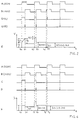
- the operation of the circuit will now be considered with reference to Figure 2, assuming that, initially, the oscillator ICO2 is delayed relative to the reference oscillator ICO1, that the outputs Q1 and Q2 of the two flip-flops are at a low level and the capacitor C is discharged.
- the flip-flop FF1 receives a switching signal and its output Q1 changes to the high level.
- the flip-flop FF2 also receives a switching signal and its output Q2 changes to the high level.
- the gate NAND has both its inputs at the high level such that a signal appears at its output which causes both flip-flops to be reset.
- phase detector 10 comprises two AND logic gates, designated AND1 and AND2, each having two inputs of which one is connected to the output, Q1 ⁇ or Q2 ⁇ , of one of the two flip-flops, and the other to the inverted output, Q2 or Q1, of the other of the two flip-flops.
- AND1 and AND2 each having two inputs of which one is connected to the output, Q1 ⁇ or Q2 ⁇ , of one of the two flip-flops, and the other to the inverted output, Q2 or Q1, of the other of the two flip-flops.
- the circuit processing the phase error signal produced by the detector 10 at its outputs C and D comprises an adding-subtracting counter, designated CNT, of which the adding input UP is connected to the output C and the subtracting input DW is connected to the output D, and a digital-to-analogue convertor, designated DAC, connected between the output of the counter CNT and the output node of the circuit, designated H, which is connected to the regulating terminal F of the oscillator ICO2.
- the counter CNT is enabled to count in the adding direction owing to the presence of a high level signal at its input UP.
- the counting speed of the counter is selected such that it is high enough to obtain a measurement of the phase displacement with the desired degree of accuracy.
- the number n1 present at the output of the counter at the instant t1 is converted into a current In1, of which the magnitude is proportional to the phase displacement and which is sent to the regulating terminal F of the oscillator ICO2 until a new phase comparison is initiated at the instant t2.
- the process is repeated in the measuring interval t3-t2 during which the adding counting terminal UP is activated once again.
- the counting of the counter passes from n1 to n2 and the regulating current Ic increases by a value In2 which is proportional to the new phase displacement measured.
- the following correction of the frequency of ICO2, in the example in question, leads to a delay of ICO1 relative to ICO2, as shown in Figure 4. Therefore, the process is repeated with an opposite sign, that is there is a low level at the output C and a high level at the output D of the phase detector, such that the generator G1 is deactivated and the generator G2 activated.
- the adding counting is deactivated and the subtracting counting of the counter CNT is activated.
- the counter could be of the type in which the counting pulses are the same as the input pulses.
- a counter which is insensitive to the simultaneous presence of two signals at its inputs could be provided instead of the logic circuit formed by the two logic gates AND1 and AND2 which prevents there being a signal simultaneously at the two outputs of the phase detector 10. In this case, however, the currents of the generators G1 and G2 would have to be equal so as not to have any effect on the regulating current when both generators are activated.
Landscapes
- Stabilization Of Oscillater, Synchronisation, Frequency Synthesizers (AREA)
Priority Applications (2)
| Application Number | Priority Date | Filing Date | Title |
|---|---|---|---|
| EP94830523A EP0711041A1 (fr) | 1994-11-03 | 1994-11-03 | Circuit de synchronisation de phase |
| JP7287679A JPH08274635A (ja) | 1994-11-03 | 1995-11-06 | 位相ロック回路 |
Applications Claiming Priority (1)
| Application Number | Priority Date | Filing Date | Title |
|---|---|---|---|
| EP94830523A EP0711041A1 (fr) | 1994-11-03 | 1994-11-03 | Circuit de synchronisation de phase |
Publications (1)
| Publication Number | Publication Date |
|---|---|
| EP0711041A1 true EP0711041A1 (fr) | 1996-05-08 |
Family
ID=8218570
Family Applications (1)
| Application Number | Title | Priority Date | Filing Date |
|---|---|---|---|
| EP94830523A Withdrawn EP0711041A1 (fr) | 1994-11-03 | 1994-11-03 | Circuit de synchronisation de phase |
Country Status (2)
| Country | Link |
|---|---|
| EP (1) | EP0711041A1 (fr) |
| JP (1) | JPH08274635A (fr) |
Cited By (7)
| Publication number | Priority date | Publication date | Assignee | Title |
|---|---|---|---|---|
| WO1997039530A1 (fr) * | 1996-04-12 | 1997-10-23 | Silicon Image, Inc. | Boucle a phase asservie a grande vitesse et haute precision |
| EP0926813A1 (fr) * | 1997-12-23 | 1999-06-30 | Hewlett-Packard Company | Détecteur de phase à modulation de largeur d'impulsion présentant une excursion de sortie étendue |
| US6435037B1 (en) | 2000-01-06 | 2002-08-20 | Data Sciences International, Inc. | Multiplexed phase detector |
| WO2001050144A3 (fr) * | 2000-01-06 | 2003-02-06 | Data Sciences Int Inc | Detecteur de phase |
| US6539316B1 (en) | 2000-01-06 | 2003-03-25 | Data Sciences International, Inc. | Phase detector |
| US6595071B1 (en) | 2000-01-06 | 2003-07-22 | Transoma Medical, Inc. | Estimation of error angle in ultrasound flow measurement |
| WO2013156060A1 (fr) * | 2012-04-17 | 2013-10-24 | Epcos Ag | Détecteur de phase de plage de 360° linéaire |
Citations (4)
| Publication number | Priority date | Publication date | Assignee | Title |
|---|---|---|---|---|
| GB2055268A (en) * | 1979-06-19 | 1981-02-25 | Tokyo Shibaura Electric Co | Digital phase comparator circuit |
| US4988955A (en) * | 1989-02-17 | 1991-01-29 | Kabushiki Kaisha Toshiba | Phase-locked loop apparatus |
| EP0585806A2 (fr) * | 1992-09-01 | 1994-03-09 | Alcatel SEL Aktiengesellschaft | Comparateur de phase numérique et boucle à verrouillage de phase |
| DE4406834A1 (de) * | 1993-03-02 | 1994-09-08 | Mitsubishi Electric Corp | PLL-Schaltung |
-
1994
- 1994-11-03 EP EP94830523A patent/EP0711041A1/fr not_active Withdrawn
-
1995
- 1995-11-06 JP JP7287679A patent/JPH08274635A/ja active Pending
Patent Citations (4)
| Publication number | Priority date | Publication date | Assignee | Title |
|---|---|---|---|---|
| GB2055268A (en) * | 1979-06-19 | 1981-02-25 | Tokyo Shibaura Electric Co | Digital phase comparator circuit |
| US4988955A (en) * | 1989-02-17 | 1991-01-29 | Kabushiki Kaisha Toshiba | Phase-locked loop apparatus |
| EP0585806A2 (fr) * | 1992-09-01 | 1994-03-09 | Alcatel SEL Aktiengesellschaft | Comparateur de phase numérique et boucle à verrouillage de phase |
| DE4406834A1 (de) * | 1993-03-02 | 1994-09-08 | Mitsubishi Electric Corp | PLL-Schaltung |
Non-Patent Citations (1)
| Title |
|---|
| SAM YINSHANG SUN: "AN ANALOG PLL-BASED CLOCK AND DATA RECOVERY CIRCUIT WITH HIGH INPUT JITTER TOLERANCE", IEEE JOURNAL OF SOLID-STATE CIRCUITS, vol. 24, no. 2, April 1989 (1989-04-01), NEW YORK US, pages 325 - 330, XP000069823 * |
Cited By (9)
| Publication number | Priority date | Publication date | Assignee | Title |
|---|---|---|---|---|
| WO1997039530A1 (fr) * | 1996-04-12 | 1997-10-23 | Silicon Image, Inc. | Boucle a phase asservie a grande vitesse et haute precision |
| US6462624B1 (en) | 1996-04-12 | 2002-10-08 | Silicon Image, Inc. | High-speed and high-precision phase locked loop |
| US6930560B2 (en) | 1996-04-12 | 2005-08-16 | Silicon Image, Inc. | High-speed and high-precision phase locked loop |
| EP0926813A1 (fr) * | 1997-12-23 | 1999-06-30 | Hewlett-Packard Company | Détecteur de phase à modulation de largeur d'impulsion présentant une excursion de sortie étendue |
| US6435037B1 (en) | 2000-01-06 | 2002-08-20 | Data Sciences International, Inc. | Multiplexed phase detector |
| WO2001050144A3 (fr) * | 2000-01-06 | 2003-02-06 | Data Sciences Int Inc | Detecteur de phase |
| US6539316B1 (en) | 2000-01-06 | 2003-03-25 | Data Sciences International, Inc. | Phase detector |
| US6595071B1 (en) | 2000-01-06 | 2003-07-22 | Transoma Medical, Inc. | Estimation of error angle in ultrasound flow measurement |
| WO2013156060A1 (fr) * | 2012-04-17 | 2013-10-24 | Epcos Ag | Détecteur de phase de plage de 360° linéaire |
Also Published As
| Publication number | Publication date |
|---|---|
| JPH08274635A (ja) | 1996-10-18 |
Similar Documents
| Publication | Publication Date | Title |
|---|---|---|
| US5136260A (en) | PLL clock synthesizer using current controlled ring oscillator | |
| US5552748A (en) | Digitally-tuned oscillator including a self-calibrating RC oscillator circuit | |
| US8306175B2 (en) | Clock and data recovery circuit | |
| US5594388A (en) | Self-calibrating RC oscillator | |
| US5740213A (en) | Differential charge pump based phase locked loop or delay locked loop | |
| US6456170B1 (en) | Comparator and voltage controlled oscillator circuit | |
| US4494021A (en) | Self-calibrated clock and timing signal generator for MOS/VLSI circuitry | |
| KR100819954B1 (ko) | 온 다이 온도 및/또는 전압 변화를 검출하는 방법 및 집적 회로 칩 | |
| US5159205A (en) | Timing generator circuit including adjustable tapped delay line within phase lock loop to control timing of signals in the tapped delay line | |
| KR920004335B1 (ko) | 전압제어발진회로 | |
| EP0692879B1 (fr) | Oscillateur en anneau avec une boucle de commande de fréquence | |
| EP0500014A2 (fr) | Détecteur de phase | |
| EP0377897A2 (fr) | Dispositif de commande de rapport cyclique | |
| US11855639B2 (en) | Slew rate control device and slew rate control method | |
| KR960001075B1 (ko) | 위상 검출기 | |
| EP0711041A1 (fr) | Circuit de synchronisation de phase | |
| US12249957B2 (en) | Self-biased, closed loop, low current free running oscillator | |
| US4598217A (en) | High speed phase/frequency detector | |
| EP0670499B1 (fr) | Convertisseur de tension en fréquence | |
| US20030179029A1 (en) | Arrangement and method for adjustment of the slope times for one or more drivers and a driver circuit | |
| US5617062A (en) | Timing circuit with rapid initialization on power-up | |
| US6091271A (en) | Frequency doubling method and apparatus | |
| EP1109317A1 (fr) | Oscillateur de commande et procédé associé | |
| US5384554A (en) | Voltage controlled oscillator circuit employing integrated circuit component ratios | |
| US5414354A (en) | Apparatus and method for generating a substantially rectangular output signal |
Legal Events
| Date | Code | Title | Description |
|---|---|---|---|
| PUAI | Public reference made under article 153(3) epc to a published international application that has entered the european phase |
Free format text: ORIGINAL CODE: 0009012 |
|
| 17P | Request for examination filed |
Effective date: 19951102 |
|
| AK | Designated contracting states |
Kind code of ref document: A1 Designated state(s): DE FR GB IT |
|
| AX | Request for extension of the european patent |
Free format text: LT;SI |
|
| RAX | Requested extension states of the european patent have changed |
Free format text: LT;SI |
|
| RAP3 | Party data changed (applicant data changed or rights of an application transferred) |
Owner name: STMICROELECTRONICS S.R.L. |
|
| 17Q | First examination report despatched |
Effective date: 19980805 |
|
| STAA | Information on the status of an ep patent application or granted ep patent |
Free format text: STATUS: THE APPLICATION IS DEEMED TO BE WITHDRAWN |
|
| 18D | Application deemed to be withdrawn |
Effective date: 19981216 |