EP0926813A1 - Détecteur de phase à modulation de largeur d'impulsion présentant une excursion de sortie étendue - Google Patents
Détecteur de phase à modulation de largeur d'impulsion présentant une excursion de sortie étendue Download PDFInfo
- Publication number
- EP0926813A1 EP0926813A1 EP98118668A EP98118668A EP0926813A1 EP 0926813 A1 EP0926813 A1 EP 0926813A1 EP 98118668 A EP98118668 A EP 98118668A EP 98118668 A EP98118668 A EP 98118668A EP 0926813 A1 EP0926813 A1 EP 0926813A1
- Authority
- EP
- European Patent Office
- Prior art keywords
- phase
- signal
- circuit
- generating
- reference signal
- Prior art date
- Legal status (The legal status is an assumption and is not a legal conclusion. Google has not performed a legal analysis and makes no representation as to the accuracy of the status listed.)
- Withdrawn
Links
- 238000001514 detection method Methods 0.000 claims abstract description 21
- 230000000295 complement effect Effects 0.000 claims description 4
- 230000004044 response Effects 0.000 claims description 3
- 238000010586 diagram Methods 0.000 description 3
- 230000008859 change Effects 0.000 description 2
- 230000000694 effects Effects 0.000 description 2
- 230000010363 phase shift Effects 0.000 description 2
- 230000008901 benefit Effects 0.000 description 1
- 238000012886 linear function Methods 0.000 description 1
- 238000005259 measurement Methods 0.000 description 1
- 230000004048 modification Effects 0.000 description 1
- 238000012986 modification Methods 0.000 description 1
- 238000007493 shaping process Methods 0.000 description 1
- 230000000087 stabilizing effect Effects 0.000 description 1
- 230000007704 transition Effects 0.000 description 1
Images


Classifications
-
- G—PHYSICS
- G01—MEASURING; TESTING
- G01R—MEASURING ELECTRIC VARIABLES; MEASURING MAGNETIC VARIABLES
- G01R25/00—Arrangements for measuring phase angle between a voltage and a current or between voltages or currents
-
- H—ELECTRICITY
- H03—ELECTRONIC CIRCUITRY
- H03D—DEMODULATION OR TRANSFERENCE OF MODULATION FROM ONE CARRIER TO ANOTHER
- H03D13/00—Circuits for comparing the phase or frequency of two mutually-independent oscillations
- H03D13/003—Circuits for comparing the phase or frequency of two mutually-independent oscillations in which both oscillations are converted by logic means into pulses which are applied to filtering or integrating means
- H03D13/004—Circuits for comparing the phase or frequency of two mutually-independent oscillations in which both oscillations are converted by logic means into pulses which are applied to filtering or integrating means the logic means delivering pulses at more than one terminal, e.g. up and down pulses
-
- H—ELECTRICITY
- H03—ELECTRONIC CIRCUITRY
- H03L—AUTOMATIC CONTROL, STARTING, SYNCHRONISATION OR STABILISATION OF GENERATORS OF ELECTRONIC OSCILLATIONS OR PULSES
- H03L7/00—Automatic control of frequency or phase; Synchronisation
- H03L7/06—Automatic control of frequency or phase; Synchronisation using a reference signal applied to a frequency- or phase-locked loop
- H03L7/08—Details of the phase-locked loop
- H03L7/081—Details of the phase-locked loop provided with an additional controlled phase shifter
-
- H—ELECTRICITY
- H03—ELECTRONIC CIRCUITRY
- H03L—AUTOMATIC CONTROL, STARTING, SYNCHRONISATION OR STABILISATION OF GENERATORS OF ELECTRONIC OSCILLATIONS OR PULSES
- H03L7/00—Automatic control of frequency or phase; Synchronisation
- H03L7/06—Automatic control of frequency or phase; Synchronisation using a reference signal applied to a frequency- or phase-locked loop
- H03L7/08—Details of the phase-locked loop
- H03L7/085—Details of the phase-locked loop concerning mainly the frequency- or phase-detection arrangement including the filtering or amplification of its output signal
- H03L7/089—Details of the phase-locked loop concerning mainly the frequency- or phase-detection arrangement including the filtering or amplification of its output signal the phase or frequency detector generating up-down pulses
Definitions
- the present invention relates to electronic circuits, and more particularly, to circuits for measuring the phase difference between two signals.
- a number of circuits utilize phase detection circuits for measuring the phase difference of two signals.
- frequency synthesizers based on phase locked loops are well known in the electronic arts. These circuits generate a signal which is a multiple of a reference frequency.
- the circuits utilize a feedback system in which the output signal's frequency is divided by X and fed to a phase detector which generates a signal indicative of the phase difference between the frequency divided output signal and the reference signal. This signal is then used to servo a voltage controlled oscillator until the output signal generated by the voltage controlled oscillator is X times the reference frequency.
- phase difference of these signals will increase linearly with time.
- prior art phase detection circuits are not capable of measuring an arbitrarily large phase difference.
- the typical phase detection circuit generates a signal that is linearly related to the phase difference until the phase difference exceeds some predetermined value, usually about 360 degrees. As the phase increases past this value, the output signal returns to zero and starts to increase again. In effect, the output of these phase detectors is roughly proportional to the phase difference modulo 360 degrees.
- phase detection circuit has a deliterious effect on the settling time of a phase lock loop frequency synthesizer.
- an integrator must be included in the phase locked loop.
- the integrator and associated stabilizing components introduce time constants which increase the settling time of the loop when the output frequency is changed or the synthesizer is first turned on.
- the non-linearities in the phase detector also result in poor settling times when the output frequency differs greatly from the desired frequency, since the servo signal generated by a 370 degree phase difference is the same as that generated by a 10 degree phase difference.
- Circuits that eliminate the "wrapping" of the phase difference signal at 360 degrees have been utilized to improve the performance of phase locked loops. These circuits generate a signal that is linearly related to the phase difference when the input signals are close in frequency. When the signals differ substantially in frequency, however, the output signal is a non-linear function of the frequency difference of the signals. Unfortunately, the non-linear relationship between the phase difference and the output signal present in these circuits also results in a significant increase in the settling time of a phase locked loop utilizing such circuits relative to the settling time that would be obtained if a linear phase detector had been utilized.
- the present invention is a circuit for generating a signal that is proportional to the phase difference between a reference signal and a variable frequency signal.
- the circuit includes a reference generating circuit for generating N phase shifted reference signals from the reference signal. Each of the phase shifted reference signals has the same frequency and a different phase.
- the phase of the n th one of the phase shifted reference signals is equal to 360n/N degrees, where N>1 and n runs from 0 to N-1.
- the reference generating circuit outputs one of the phase shifted reference signals at any given time.
- a phase detection circuit connected to the reference generating circuit, generates a phase output signal proportional to the phase difference between the variable frequency signal and the current phase shifted reference signal.
- the phase output signal has value of I when the output signal corresponds to a phase difference of 360/N degrees.
- An overflow detection circuit determines when the phase output signal has an absolute value greater than I.
- the overflow detection circuit generates a count signal and a phase adjustment signal when this situation is detected.
- the phase adjustment signal is coupled to the reference generating circuit and causes the reference generating circuit to output a new reference signal.
- a counter coupled to the overflow detection circuit, holds a digital value which is incremented or decremented in response to the count signal.
- a digital to analog converter converts the digital value in the counter to a signal having an amplitude equal to MI, where M is the digital value.
- a sum circuit adds the signal generated by the digital to analog converter to the phase output signal.
- phase difference for phase differences of less than 360 degrees are known and operate adequately.
- phase difference may be represented as a multiple of a predetermined phase difference less than 360 degrees plus a residual phase difference which is less than 360 degrees.
- Phase detector 10 generates two signals, PU and PD. Each of these signals has a pulse width that is proportional to the phase difference between F ref and F x over the range of phase differences discussed below. If the reference signal leads F x , PU represents the phase difference. If reference signal lags F x , PD represents the phase difference.
- the pulse width of the PU or PD signal is proportional to the phase difference between F ref and F x . Outside of this range, the outputs will no longer be proportional to the total phase differences. For example, if F ref is much higher than F x , then a second leading edge of F ref can arrive at flip-flop 11 before a leading edge of F x resets the phase detector. For any given maximum difference in frequencies, there will always be a range of times over which the PU and PD signals are proportional to the phase difference.
- the present invention makes use of this linear range by adjusting the phase of F ref periodically such that the phase difference between F ref and F x is always within the linear range of the phase detector.
- the accumulated phase adjustment is stored in a register that is used to generate a current representing the accumulated phase adjustment.
- the output of the phase detector is also converted to a current which is proportional to the pulse width of the PU or PD signals. These two currents are then added to obtain a current that is proportional to the total phase difference between the two signals.
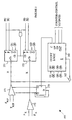
- FIG. 2 is a block diagram of a phase measuring circuit 20 according to the present invention.
- Circuit 20 generates an output signal which is proportional to the phase difference between a reference signal F ref and a signal F x whose phase and frequency is assumed to be variable.
- Phase detector 22 measures the phase difference between an adjusted reference signal F' ref and F x in a manner analogous to phase detector 10 discussed above.
- the adjusted reference signal is generated by adding or subtracting predetermined phase increments to F ref using phase adjustment circuit 21.
- phase adjustment circuit 21 operates will be explained in more detail below.
- the phase increments are 360/N degrees, and hence, phase adjustment circuit 21 selects one of the N signals generated by adding 360n/N to F ref .
- n runs from 0 to N-1.
- An overflow detection circuit 24 monitors the output of phase detector 22 to determine if the phase difference between F' ref and F x has an absolute value greater than 360/N. If overflow detector 24 detects a phase difference that is outside of this range, it generates a signal, CU or CD, which indicates this condition and whether the phase difference is less than - 360/N (i.e., CU) or greater than +360/N (i.e., CD). CU causes register 25 to be incremented and phase adjust circuit 21 to subtract 360/N from the phase of F' ref . Similarly, CD causes register 25 to be decremented and 360/N to be added to the phase of F' ref .
- phase measuring circuit 20 is generated by a sum circuit 27 which adds the phase difference detected by phase detector 22 to a current which is proportional to the count in register 25.
- a current converter 23 converts the pulse width of the PU and PD to an average current in a range from -I to I.
- digital to analog converter 26 converts the count in register 25 to current equal to MI, where M is the count stored in register 25. It should be noted that M may be negative.
- the output of the analog to digital converter can be offset by a fixed current, thereby allowing only positive M values to be used. The later alternative has the advantage of not requiring a bi-polar analog to digital converter.
- phase difference is held between -I and I.
- phase difference is held between any two values separated by 2I may also be constructed.
- Such embodiments are equivalent to offsetting the phase of the reference signal by a constant value. Since the "zero" phase of the reference signal is arbitrary, such an offset does not change the operation of the invention.
- phase detector 22 shown in Figure 2 The function provided by phase detector 22 shown in Figure 2 is provided by a phase detector circuit 53 which operates in a manner analogous to the circuit shown in Figure 1.
- a signal PU When F x lags in phase relative to F' ref , a signal PU is generated having a pulse width that is proportional to the phase difference.
- a signal PD When F x leads F' ref , a signal PD is generated having a pulse width that is proportional to the phase difference.
- Overflow circuit 52 monitors the pulse width of PU and PD to determine if the phase difference between F x and F' ref exceeds 180 degrees.
- circuit 52 detects a phase difference in excess of 180 degrees it generates CU or CD, depending on whether the phase difference is positive or negative, and then toggles multiplexer 51.
- the phase difference is negative, i.e., PU is active, having a pulse width which is proportional to the phase difference.
- Flip-flop 54 samples the PU signal on the falling edge of F' ref . If the phase difference is greater than 180 degrees, PU will still be high on the falling edge of F' ref . Hence, the output of flip-flop 54 will go high, and CU will also be generated.
- CU will cause the multiplexer 51 to switch to the alternative signal for F' ref , thereby changing the phase of F' ref by 180 degrees. This will reduce the pulse width of PU, thereby returning it to a value less corresponding to a phase difference of less than 180 degrees.
- Flip-flop 55 performs the analogous comparison when PD is active, i.e., F' ref lags F x .
- Phase tracking circuit 70 differs from circuit 50 in that preamplifiers shown at 71 and 72 are used to convert the signals to square waves. In addition, the preamplifiers are run in a differential mode to reduce noise interference. Finally, the multiplexing function has been incorporated in preamplifier 71. The use of preamplifiers for both the reference and variable signal preserves the symmetry of the circuit which improves the accuracy of the phase measurements.
- phase tracking circuits described above will operate satisfactorily, there is a small problem in the cases in which the phase difference is very close to 180 degrees.
- both CU and CD may be asserted simultaneously.
- the problem arises from the fact that the PU and PD are both asserted near the trailing edge of a PU cycle, prior to flip-flop resets.
- Phase tracking circuit 100 assumes that F ref and F x are sinusoids. These signals are amplified to sharp logic levels by differential-input preamplifiers 171 and 172, respectively. Preamplifiers 171 and 172 have selectable polarity. The selectable polarity of preamplifier 171 is used to change the phase of the reference signal R by 180 degrees when either PU or PD exceeds a phase shift of 180 degrees. Preamplifier 172 is implemented with an identical preamplifier to improve the accuracy of phase tracking circuit 171; however, the selectable polarity feature of preamplifier 172 is not utilized.
- the logic signals R and X are used to drive flip-flops 151 and 152 which generate two sets of output signals.
- the signals PU and PD have pulse widths that are proportional to the phase difference between F ref and F x .
- the logically similar signals QU and QD are used to detect the cases in which one of these signals represents a phase difference of greater than 180 degrees.
- Signals PU and PU are overlapping-low, i.e., when PU goes low, PU remains low until PU finishes its transition.
- Signals QU and QU are overlapping-high.
- the counting logic 180 differs from the embodiments shown above in that the signals CU and CD have been replaced by a count signal C and a direction signal UP which indicates whether the counter is to be incremented or decremented.
- the count signal drives flip-flop 173 which controls the phase of R.
- the counting logic is shown in more detail in Figure 6.
- the detection of a phase shift greater than 180 degrees is performed by flip-flops 181 and 182 which operate in a manner analogous to that discussed above with reference to flip-flops 54 and 55.
- These flip-flops are driven with signals derived from the QU and QD signals by NOR gates 187 and 188 to prevent CU and CD from being asserted simultaneously when the phase difference between R and X is near 180 degrees.
- the CU and CD signals are converted to the C and UP signals discussed above by latch 183 and gate 184.
- a second count signal, DAC is formed from C by utilizing delay circuit 185 and pulse shaping circuit 186. DAC is used to strobe the counter. The delay and pulse lengthening assure that the signal is not asserted until UP has settled and that the signal is of sufficient duration to properly increment the counter.
- the various phase shifted reference signals may be generated by a frequency dividing a higher frequency reference signal.
- a multiplexer selects between the N phase shifted reference such that each time the phase signal from the phase measuring circuit moves outside of the ⁇ 360/N degree range, the next higher or lower phase reference signal is selected for input to the phase measuring circuit.
- phase detection circuit that provides a signal that is proportional to the phase difference between the phase shifted reference signal and the variable frequency signal.
- strict proportionality is not required. So long as the output of the phase detection circuit is monotonically related to the phase difference and the points at which the absolute value of the phase difference exceeds 360/N are detectable, a workable system can be constructed. In such a system, any non-linearities can be corrected by providing a calibration circuit as part of current converter 23 shown in Figure 2. Furthermore, if N is sufficiently large, the current converter can be eliminated in systems which do not require an accuracy of more than 360/N.
Landscapes
- Engineering & Computer Science (AREA)
- Power Engineering (AREA)
- Physics & Mathematics (AREA)
- General Physics & Mathematics (AREA)
- Measuring Phase Differences (AREA)
- Manipulation Of Pulses (AREA)
- Stabilization Of Oscillater, Synchronisation, Frequency Synthesizers (AREA)
Applications Claiming Priority (2)
| Application Number | Priority Date | Filing Date | Title |
|---|---|---|---|
| US997148 | 1997-12-23 | ||
| US08/997,148 US5952853A (en) | 1997-12-23 | 1997-12-23 | Method for extending the output range of pulse-width based phase detectors |
Publications (1)
| Publication Number | Publication Date |
|---|---|
| EP0926813A1 true EP0926813A1 (fr) | 1999-06-30 |
Family
ID=25543697
Family Applications (1)
| Application Number | Title | Priority Date | Filing Date |
|---|---|---|---|
| EP98118668A Withdrawn EP0926813A1 (fr) | 1997-12-23 | 1998-10-02 | Détecteur de phase à modulation de largeur d'impulsion présentant une excursion de sortie étendue |
Country Status (3)
| Country | Link |
|---|---|
| US (1) | US5952853A (fr) |
| EP (1) | EP0926813A1 (fr) |
| JP (1) | JPH11289249A (fr) |
Families Citing this family (12)
| Publication number | Priority date | Publication date | Assignee | Title |
|---|---|---|---|---|
| US6137852A (en) * | 1997-12-23 | 2000-10-24 | Motorola, Inc | Phase detector circuit and method of phase detecting |
| JP3554514B2 (ja) | 1999-12-03 | 2004-08-18 | 松下電器産業株式会社 | 半導体装置及びその製造方法 |
| US20020093986A1 (en) * | 2000-12-30 | 2002-07-18 | Norm Hendrickson | Forward data de-skew method and system |
| US20020093994A1 (en) * | 2000-12-30 | 2002-07-18 | Norm Hendrickson | Reverse data de-skew method and system |
| US20020090045A1 (en) * | 2001-01-10 | 2002-07-11 | Norm Hendrickson | Digital clock recovery system |
| US7123678B2 (en) | 2001-02-01 | 2006-10-17 | Vitesse Semiconductor Corporation | RZ recovery |
| FI114886B (fi) * | 2001-06-29 | 2005-01-14 | Nokia Corp | Menetelmä ja laite taajuussyntetisaattorin tehokkuuden parantamiseksi |
| US7567642B2 (en) * | 2003-12-23 | 2009-07-28 | Analog Devices, Inc. | Phase detector with extended linear operating range |
| JP5573628B2 (ja) | 2010-11-22 | 2014-08-20 | 富士通株式会社 | 位相差検出方法、位相制御方法、位相差検出回路、位相制御回路及び無線電力伝送装置 |
| JP2012165187A (ja) * | 2011-02-07 | 2012-08-30 | Fujitsu Telecom Networks Ltd | Pll回路 |
| JP2014124052A (ja) * | 2012-12-21 | 2014-07-03 | Hioki Ee Corp | 圧電トランス駆動回路 |
| CN104360159A (zh) * | 2014-11-19 | 2015-02-18 | 国网浙江余姚市供电公司 | 核相方法及装置 |
Citations (5)
| Publication number | Priority date | Publication date | Assignee | Title |
|---|---|---|---|---|
| US4520321A (en) * | 1981-11-30 | 1985-05-28 | Anritsu Electric Company Limited | Phase difference detector with phase inversion of one input signal when phase difference is small |
| EP0256637A2 (fr) * | 1986-08-02 | 1988-02-24 | Marconi Instruments Limited | Détecteur de phase |
| US4988955A (en) * | 1989-02-17 | 1991-01-29 | Kabushiki Kaisha Toshiba | Phase-locked loop apparatus |
| US5307020A (en) * | 1991-03-22 | 1994-04-26 | Thomson-Csf | Phase comparator device with wide dynamic range |
| EP0711041A1 (fr) * | 1994-11-03 | 1996-05-08 | STMicroelectronics S.r.l. | Circuit de synchronisation de phase |
Family Cites Families (4)
| Publication number | Priority date | Publication date | Assignee | Title |
|---|---|---|---|---|
| US4767945A (en) * | 1986-10-14 | 1988-08-30 | Tektronix, Inc. | Analog signal multiplexer |
| US5451894A (en) * | 1993-02-24 | 1995-09-19 | Advanced Micro Devices, Inc. | Digital full range rotating phase shifter |
| US5491673A (en) * | 1994-06-02 | 1996-02-13 | Advantest Corporation | Timing signal generation circuit |
| JP2933016B2 (ja) * | 1996-04-02 | 1999-08-09 | 横河電機株式会社 | 渦流量計 |
-
1997
- 1997-12-23 US US08/997,148 patent/US5952853A/en not_active Expired - Lifetime
-
1998
- 1998-10-02 EP EP98118668A patent/EP0926813A1/fr not_active Withdrawn
- 1998-12-18 JP JP10360370A patent/JPH11289249A/ja active Pending
Patent Citations (5)
| Publication number | Priority date | Publication date | Assignee | Title |
|---|---|---|---|---|
| US4520321A (en) * | 1981-11-30 | 1985-05-28 | Anritsu Electric Company Limited | Phase difference detector with phase inversion of one input signal when phase difference is small |
| EP0256637A2 (fr) * | 1986-08-02 | 1988-02-24 | Marconi Instruments Limited | Détecteur de phase |
| US4988955A (en) * | 1989-02-17 | 1991-01-29 | Kabushiki Kaisha Toshiba | Phase-locked loop apparatus |
| US5307020A (en) * | 1991-03-22 | 1994-04-26 | Thomson-Csf | Phase comparator device with wide dynamic range |
| EP0711041A1 (fr) * | 1994-11-03 | 1996-05-08 | STMicroelectronics S.r.l. | Circuit de synchronisation de phase |
Also Published As
| Publication number | Publication date |
|---|---|
| US5952853A (en) | 1999-09-14 |
| JPH11289249A (ja) | 1999-10-19 |
Similar Documents
| Publication | Publication Date | Title |
|---|---|---|
| US5774023A (en) | Adaptive phase locked loop system with charge pump having dual current output | |
| US5952853A (en) | Method for extending the output range of pulse-width based phase detectors | |
| JP3804763B2 (ja) | デューティサイクル補正回路及び方法 | |
| US8036300B2 (en) | Dual loop clock recovery circuit | |
| US6380811B1 (en) | Signal generator, and method | |
| KR100473813B1 (ko) | 다중 위상 클럭을 위한 디지털 듀티 사이클 보정 회로 및그 방법 | |
| US8437441B2 (en) | Phase locked loop capable of fast locking | |
| EP1780892B1 (fr) | Procédé de fonctionnement d'une boucle à verrouillage de phase résistante aux effets de rayonnement | |
| CN114499504A (zh) | 锁相环电路及其操作方法以及子范围控制电路 | |
| WO2001067597A1 (fr) | Preamplificateur | |
| US5999027A (en) | Phase compensating apparatus and delay controlling circuit | |
| IE61813B1 (en) | "Phase Detector" | |
| EP0414392B1 (fr) | Détecteur de phase | |
| US5302908A (en) | High precision phase comparator and phase locked loop | |
| US5831423A (en) | Phase meter and method of providing a voltage indicative of a phase difference | |
| US6525577B2 (en) | Apparatus and method for reducing skew of a high speed clock signal | |
| US7382169B2 (en) | Systems and methods for reducing static phase error | |
| KR20050091035A (ko) | 가변 딜레이 및 이산적 딜레이를 포함하는 위상 동기 루프 | |
| US7323922B1 (en) | Digitally controlled gain stage having an analogue control input | |
| US6029055A (en) | Frequency stabilization circuit using signal level threshold | |
| US6975695B1 (en) | Circuit for correction of differential signal path delays in a PLL | |
| JP4413307B2 (ja) | Pll回路 | |
| US6577695B1 (en) | Emulating narrow band phase-locked loop behavior on a wide band phase-locked loop | |
| NL8205016A (nl) | Digitaal lusfilter. | |
| US7333568B2 (en) | Data slicer capable of calibrating current mismatch |
Legal Events
| Date | Code | Title | Description |
|---|---|---|---|
| PUAI | Public reference made under article 153(3) epc to a published international application that has entered the european phase |
Free format text: ORIGINAL CODE: 0009012 |
|
| AK | Designated contracting states |
Kind code of ref document: A1 Designated state(s): DE FR GB |
|
| AX | Request for extension of the european patent |
Free format text: AL;LT;LV;MK;RO;SI |
|
| 17P | Request for examination filed |
Effective date: 19991118 |
|
| AKX | Designation fees paid |
Free format text: DE FR GB |
|
| RAP1 | Party data changed (applicant data changed or rights of an application transferred) |
Owner name: AGILENT TECHNOLOGIES, INC. |
|
| RAP1 | Party data changed (applicant data changed or rights of an application transferred) |
Owner name: AGILENT TECHNOLOGIES INC. |
|
| RAP1 | Party data changed (applicant data changed or rights of an application transferred) |
Owner name: AGILENT TECHNOLOGIES INC. A DELAWARE CORPORATION |
|
| RAP1 | Party data changed (applicant data changed or rights of an application transferred) |
Owner name: AGILENT TECHNOLOGIES, INC. (A DELAWARE CORPORATION |
|
| 17Q | First examination report despatched |
Effective date: 20040217 |
|
| STAA | Information on the status of an ep patent application or granted ep patent |
Free format text: STATUS: THE APPLICATION IS DEEMED TO BE WITHDRAWN |
|
| 18D | Application deemed to be withdrawn |
Effective date: 20040629 |