EP0711045A1 - Circuit de dérivation de photocourant en excès pour récepteur optique - Google Patents
Circuit de dérivation de photocourant en excès pour récepteur optique Download PDFInfo
- Publication number
- EP0711045A1 EP0711045A1 EP95116490A EP95116490A EP0711045A1 EP 0711045 A1 EP0711045 A1 EP 0711045A1 EP 95116490 A EP95116490 A EP 95116490A EP 95116490 A EP95116490 A EP 95116490A EP 0711045 A1 EP0711045 A1 EP 0711045A1
- Authority
- EP
- European Patent Office
- Prior art keywords
- circuit
- amplifier
- coupled
- photodetector
- diode
- Prior art date
- Legal status (The legal status is an assumption and is not a legal conclusion. Google has not performed a legal analysis and makes no representation as to the accuracy of the status listed.)
- Withdrawn
Links
- 230000003287 optical effect Effects 0.000 title abstract description 8
- 239000003990 capacitor Substances 0.000 description 7
- 101710170230 Antimicrobial peptide 1 Proteins 0.000 description 3
- 238000004891 communication Methods 0.000 description 3
- 230000035945 sensitivity Effects 0.000 description 3
- 101710170231 Antimicrobial peptide 2 Proteins 0.000 description 2
- 230000009977 dual effect Effects 0.000 description 2
- 238000000034 method Methods 0.000 description 2
- 230000003321 amplification Effects 0.000 description 1
- 238000013459 approach Methods 0.000 description 1
- 230000008878 coupling Effects 0.000 description 1
- 238000010168 coupling process Methods 0.000 description 1
- 238000005859 coupling reaction Methods 0.000 description 1
- 238000013461 design Methods 0.000 description 1
- 238000012986 modification Methods 0.000 description 1
- 230000004048 modification Effects 0.000 description 1
- 238000003199 nucleic acid amplification method Methods 0.000 description 1
Images
Classifications
-
- H—ELECTRICITY
- H04—ELECTRIC COMMUNICATION TECHNIQUE
- H04B—TRANSMISSION
- H04B10/00—Transmission systems employing electromagnetic waves other than radio-waves, e.g. infrared, visible or ultraviolet light, or employing corpuscular radiation, e.g. quantum communication
- H04B10/60—Receivers
Definitions
- the invention relates to optical receivers, and in particular to a circuit for shunting excess photocurrent in such circuits.
- Optical receivers used in infrared (IR) communication typically consist of a photodiode which converts optical signals to electrical current followed by one or more amplification stages and a decision circuit to convert the amplified analog signal to digital format.
- Such receivers used for IR wireless applications must operate over a wide range of input signal levels. Ideally, one would like a receiver with high-gain to allow communication for a distance of a meter or more while at the same time allowing close-proximity communication where the optical signal can be more than 100,000 times larger.
- AGC Automatic Gain Control
- Another method of providing a large dynamic range is to use a fixed the decision threshold. With this method, however, a reduction in sensitivity results because the threshold must be set to a worst-case value. However, increasing the current (the bias point of the transistors, for example) also increases noise in the circuit (as well as power dissipation) and tends to reduce the sensitivity of the receiver.
- the present invention solves the above problems and aims at providing a low-power circuit with excellent sensitivity while also allowing wide dynamic range. We accomplish this by shunting excess photocurrent at the input of the first amplifier stage, thereby effectively "clamping" the maximum photocurrent which the amplifiers see.
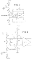
- FIG. 1 A preferred implementation of this clamp circuit is shown in FIG. 1.
- the circuit comprises a photodiode D2, resistors R1 and R2 coupled to the cathode of the photodiode, a capacitor C2 coupled to the junction of resistors R1 and R2, a resistor R3 coupled to the anode of photodiode D2, and a dual input amplifier circuit A1 coupled across the photodiode.
- the dual input amplifier is connected across the diode via coupling capacitors C2 and C3 to remove DC bias.
- Matched enhancement mode FETs Q1 and Q2 are connected across the inputs to an amplifier AMP1, as shown.
- matched FETs and transistors are available (for example, by designing an ASIC).
- the outputs of the amplifier AMP1 are each coupled to a gate of a different one of the FETs Q1, Q2.
- the circuit of FIG.1 employs a feedback amplifier AMP1 (e.g., transimpedance) wherein the signals at the output of the amplifier are used to switch on the FETs Q1, Q2 when the voltage exceeds the FET threshold voltage. When the FETs turn on, any excess photocurrent is shorted and prevented from entering the amplifier.
- AMP1 e.g., transimpedance
- an inverting differential amplifier can be used with NFETs, configured as shown in FIG. 1.
- NFETs configured as shown in FIG. 1.
- FIG. 2 is another preferred embodiment of the invention.
- the circuit comprises an amplifier AMP2, having inputs capacitively coupled via capacitors C3 and C4 across photodiode D2.
- the cathode of D2 is biased to a level determined by the voltage divider comprising resistors R8, R9 and R10.
- Also capacitively coupled across the photodiode D2, via capacitors C5 and C6, is a diode D7.
- D7 is a schottky diode. It will be understood, however, that in circuits in which the photodiode has a sufficiently high capacitance, the schottky diode of the preferred embodiment can be replaced with any other suitable diode.
- diode D7 has a resistor R4 coupled to the anode thereof.
- Diode D7 and resistor R4 are coupled across a voltage divider comprising resistors R5, R6 and R7.
- the voltage divider is connected between ground and +V cc .
- the voltage divider is also capacitively coupled to ground via capacitor C7.
- the circuit of FIG. 2 is particularly useful in the case where matched FETs are not available.
- a shunting circuit employing a schottky diode D7.
- the schottky D7 is ac coupled to the photodiode D2 via capacitors C1, C2 and biased by the voltage divider network (RS1, RS2, RP) near the turn-on of the schottky D7.
- RS1, RS2, RP voltage divider network
- the voltage applied to the schottky can be adjusted through the voltage divider to allow switching at the desired input signal level.
- the resistor R4 prevents the impedance of the shorting circuit (comprising D7 and R4) from dropping too low during switching, and the resistor parallel to the schottky, R6, discharges capacitors C5 and C6 at a frequency lower than the high-pass frequency of the ac coupled amplifier input.
- a second diode/resistor can be added across D7 and R4. This will allow the circuit to clamp both positive and negative pulses.
- the embodiment depicted in FIG. 1 could be modified by removing either Q1 or Q2, in which case the circuit would clamp only positive or negative pulses.
Landscapes
- Physics & Mathematics (AREA)
- Electromagnetism (AREA)
- Engineering & Computer Science (AREA)
- Computer Networks & Wireless Communication (AREA)
- Signal Processing (AREA)
- Amplifiers (AREA)
- Optical Communication System (AREA)
Applications Claiming Priority (2)
| Application Number | Priority Date | Filing Date | Title |
|---|---|---|---|
| US33466494A | 1994-11-04 | 1994-11-04 | |
| US334664 | 1994-11-04 |
Publications (1)
| Publication Number | Publication Date |
|---|---|
| EP0711045A1 true EP0711045A1 (fr) | 1996-05-08 |
Family
ID=23308222
Family Applications (1)
| Application Number | Title | Priority Date | Filing Date |
|---|---|---|---|
| EP95116490A Withdrawn EP0711045A1 (fr) | 1994-11-04 | 1995-10-19 | Circuit de dérivation de photocourant en excès pour récepteur optique |
Country Status (2)
| Country | Link |
|---|---|
| EP (1) | EP0711045A1 (fr) |
| JP (1) | JPH08213852A (fr) |
Cited By (3)
| Publication number | Priority date | Publication date | Assignee | Title |
|---|---|---|---|---|
| WO2006099899A1 (fr) * | 2005-03-21 | 2006-09-28 | Helix Ag | Recepteur optique symetrique |
| WO2020061970A1 (fr) * | 2018-09-27 | 2020-04-02 | 深圳市大疆创新科技有限公司 | Dispositif de télémétrie et plateforme mobile |
| WO2023148207A1 (fr) * | 2022-02-01 | 2023-08-10 | Universität Paderborn | Mélangeur électro-optique |
Citations (5)
| Publication number | Priority date | Publication date | Assignee | Title |
|---|---|---|---|---|
| JPS5583312A (en) * | 1978-12-20 | 1980-06-23 | Fujitsu Ltd | Agc circuit |
| JPS62217738A (ja) * | 1986-03-19 | 1987-09-25 | Nec Corp | 光受信回路 |
| EP0246662A1 (fr) * | 1986-05-23 | 1987-11-25 | Siemens Aktiengesellschaft | Récepteur pour signaux numériques optiques d'amplitudes différentes |
| DE3824494A1 (de) * | 1988-07-20 | 1990-01-25 | Philips Patentverwaltung | Optischer empfaenger |
| US5013903A (en) * | 1990-02-26 | 1991-05-07 | At&T Bell Laboratories | Lightwave receiver having differential input |
-
1995
- 1995-10-19 EP EP95116490A patent/EP0711045A1/fr not_active Withdrawn
- 1995-10-26 JP JP7279241A patent/JPH08213852A/ja active Pending
Patent Citations (5)
| Publication number | Priority date | Publication date | Assignee | Title |
|---|---|---|---|---|
| JPS5583312A (en) * | 1978-12-20 | 1980-06-23 | Fujitsu Ltd | Agc circuit |
| JPS62217738A (ja) * | 1986-03-19 | 1987-09-25 | Nec Corp | 光受信回路 |
| EP0246662A1 (fr) * | 1986-05-23 | 1987-11-25 | Siemens Aktiengesellschaft | Récepteur pour signaux numériques optiques d'amplitudes différentes |
| DE3824494A1 (de) * | 1988-07-20 | 1990-01-25 | Philips Patentverwaltung | Optischer empfaenger |
| US5013903A (en) * | 1990-02-26 | 1991-05-07 | At&T Bell Laboratories | Lightwave receiver having differential input |
Non-Patent Citations (2)
| Title |
|---|
| PATENT ABSTRACTS OF JAPAN vol. 12, no. 80 (E - 590) * |
| PATENT ABSTRACTS OF JAPAN vol. 4, no. 130 (E - 025) * |
Cited By (7)
| Publication number | Priority date | Publication date | Assignee | Title |
|---|---|---|---|---|
| WO2006099899A1 (fr) * | 2005-03-21 | 2006-09-28 | Helix Ag | Recepteur optique symetrique |
| WO2020061970A1 (fr) * | 2018-09-27 | 2020-04-02 | 深圳市大疆创新科技有限公司 | Dispositif de télémétrie et plateforme mobile |
| WO2023148207A1 (fr) * | 2022-02-01 | 2023-08-10 | Universität Paderborn | Mélangeur électro-optique |
| CN118591758A (zh) * | 2022-02-01 | 2024-09-03 | 帕德博恩大学 | 电光混合器 |
| JP2025504993A (ja) * | 2022-02-01 | 2025-02-19 | ウニヴェルシタット パダーボーン | 電気光学混合器 |
| CN118591758B (zh) * | 2022-02-01 | 2025-05-02 | 帕德博恩大学 | 电光混合器 |
| US12379617B2 (en) | 2022-02-01 | 2025-08-05 | Universität Paderborn | Electro-optical mixer |
Also Published As
| Publication number | Publication date |
|---|---|
| JPH08213852A (ja) | 1996-08-20 |
Similar Documents
| Publication | Publication Date | Title |
|---|---|---|
| US5329115A (en) | Optical receiver circuit | |
| US4764732A (en) | Switchable mode amplifier for wide dynamic range | |
| EP0181146B1 (fr) | Amplificateur d'impédance de transfert | |
| US5030925A (en) | Transimpedance amplifier | |
| US5532471A (en) | Optical transimpedance amplifier with high dynamic range | |
| KR100701741B1 (ko) | 검출 회로 | |
| US4498001A (en) | Transimpedance amplifier for optical receivers | |
| US6275114B1 (en) | Impedance matched CMOS transimpedance amplifier for high-speed fiber optic communications | |
| US6275541B1 (en) | Digital receiver circuit | |
| US5012202A (en) | Low impedance automatic gain control circuit | |
| US5844445A (en) | Feedback type pre-amplifier | |
| US4724315A (en) | Optical receiver | |
| US5343160A (en) | Fully balanced transimpedance amplifier with low noise and wide bandwidth | |
| US5734300A (en) | Optical receiver preamplifier dynamic range enhancing circuit and method | |
| JPH06177664A (ja) | ディジタル光受信回路とトランスインピーダンスアンプ回路とプリアンプ回路 | |
| CA2106439A1 (fr) | Recepteur de donnees numeriques en salves | |
| CA2128894A1 (fr) | Recepteur optique | |
| US6140878A (en) | Transimpedance-type amplifier circuit with interchangeable resistance | |
| US5111324A (en) | Optical receivers | |
| EP0433468B1 (fr) | Convertisseur de courant en tension | |
| US6876260B2 (en) | Elevated front-end transimpedance amplifier | |
| US4817208A (en) | Fiber optic receiver | |
| US4142110A (en) | Circuit to eliminate DC bias | |
| US5373388A (en) | AC coupled fiber optic receiver with DC coupled characteristics | |
| JPH08213852A (ja) | 光受信機の過剰な光電流を分路する回路 |
Legal Events
| Date | Code | Title | Description |
|---|---|---|---|
| PUAI | Public reference made under article 153(3) epc to a published international application that has entered the european phase |
Free format text: ORIGINAL CODE: 0009012 |
|
| AK | Designated contracting states |
Kind code of ref document: A1 Designated state(s): DE FR GB |
|
| STAA | Information on the status of an ep patent application or granted ep patent |
Free format text: STATUS: THE APPLICATION IS DEEMED TO BE WITHDRAWN |
|
| 18D | Application deemed to be withdrawn |
Effective date: 19961109 |