EP0713165A1 - Spannungserhöhungsschaltung für Speichervorrichtung - Google Patents
Spannungserhöhungsschaltung für Speichervorrichtung Download PDFInfo
- Publication number
- EP0713165A1 EP0713165A1 EP95308017A EP95308017A EP0713165A1 EP 0713165 A1 EP0713165 A1 EP 0713165A1 EP 95308017 A EP95308017 A EP 95308017A EP 95308017 A EP95308017 A EP 95308017A EP 0713165 A1 EP0713165 A1 EP 0713165A1
- Authority
- EP
- European Patent Office
- Prior art keywords
- voltage
- signal
- circuit
- boost
- supply
- Prior art date
- Legal status (The legal status is an assumption and is not a legal conclusion. Google has not performed a legal analysis and makes no representation as to the accuracy of the status listed.)
- Withdrawn
Links
- 230000015654 memory Effects 0.000 claims abstract description 32
- 238000000034 method Methods 0.000 claims abstract description 17
- 238000001514 detection method Methods 0.000 claims description 23
- 230000007704 transition Effects 0.000 description 45
- 230000004044 response Effects 0.000 description 24
- 239000003990 capacitor Substances 0.000 description 14
- 238000010586 diagram Methods 0.000 description 6
- PWPJGUXAGUPAHP-UHFFFAOYSA-N lufenuron Chemical compound C1=C(Cl)C(OC(F)(F)C(C(F)(F)F)F)=CC(Cl)=C1NC(=O)NC(=O)C1=C(F)C=CC=C1F PWPJGUXAGUPAHP-UHFFFAOYSA-N 0.000 description 6
- 230000009471 action Effects 0.000 description 5
- 230000008859 change Effects 0.000 description 5
- 230000001419 dependent effect Effects 0.000 description 4
- 230000000694 effects Effects 0.000 description 4
- 230000000295 complement effect Effects 0.000 description 3
- 230000000630 rising effect Effects 0.000 description 3
- 230000001808 coupling effect Effects 0.000 description 2
- 230000006870 function Effects 0.000 description 2
- 230000001172 regenerating effect Effects 0.000 description 2
- 238000009825 accumulation Methods 0.000 description 1
- 238000004883 computer application Methods 0.000 description 1
- 230000008878 coupling Effects 0.000 description 1
- 238000010168 coupling process Methods 0.000 description 1
- 238000005859 coupling reaction Methods 0.000 description 1
- 230000001934 delay Effects 0.000 description 1
- 230000005684 electric field Effects 0.000 description 1
- 230000008569 process Effects 0.000 description 1
- 230000000644 propagated effect Effects 0.000 description 1
- 230000009467 reduction Effects 0.000 description 1
- 239000000758 substrate Substances 0.000 description 1
- 230000001960 triggered effect Effects 0.000 description 1
Images




Classifications
-
- G—PHYSICS
- G05—CONTROLLING; REGULATING
- G05F—SYSTEMS FOR REGULATING ELECTRIC OR MAGNETIC VARIABLES
- G05F3/00—Non-retroactive systems for regulating electric variables by using an uncontrolled element, or an uncontrolled combination of elements, such element or such combination having self-regulating properties
- G05F3/02—Regulating voltage or current
- G05F3/08—Regulating voltage or current wherein the variable is DC
- G05F3/10—Regulating voltage or current wherein the variable is DC using uncontrolled devices with non-linear characteristics
- G05F3/16—Regulating voltage or current wherein the variable is DC using uncontrolled devices with non-linear characteristics being semiconductor devices
- G05F3/20—Regulating voltage or current wherein the variable is DC using uncontrolled devices with non-linear characteristics being semiconductor devices using diode- transistor combinations
- G05F3/24—Regulating voltage or current wherein the variable is DC using uncontrolled devices with non-linear characteristics being semiconductor devices using diode- transistor combinations wherein the transistors are of the field-effect type only
- G05F3/242—Regulating voltage or current wherein the variable is DC using uncontrolled devices with non-linear characteristics being semiconductor devices using diode- transistor combinations wherein the transistors are of the field-effect type only with compensation for device parameters, e.g. channel width modulation, threshold voltage, processing, or external variations, e.g. temperature, loading, supply voltage
- G05F3/247—Regulating voltage or current wherein the variable is DC using uncontrolled devices with non-linear characteristics being semiconductor devices using diode- transistor combinations wherein the transistors are of the field-effect type only with compensation for device parameters, e.g. channel width modulation, threshold voltage, processing, or external variations, e.g. temperature, loading, supply voltage producing a voltage or current as a predetermined function of the supply voltage
-
- G—PHYSICS
- G11—INFORMATION STORAGE
- G11C—STATIC STORES
- G11C8/00—Arrangements for selecting an address in a digital store
- G11C8/08—Word line control circuits, e.g. drivers, boosters, pull-up circuits, pull-down circuits, precharging circuits, for word lines
Definitions
- This invention relates to an integrated circuit device, and in particular to improved circuitry for boosting a signal level within an integrated circuit device above the level of the voltage supply.
- the invention is particularly, but not exclusively, concerned with a memory device in which memory cells are formed by insulated gate transistors.
- These memories include EPROMS and FLASH EPROMS referred to herein as flash memories.
- Flash memories having low voltage supplies of 3.3V ⁇ 0.3V introduce biasing problems in reading erased cells.
- the threshold voltages of erased cells ie the gate voltage required to turn the transistor in the cell on when the source is grounded
- erased cells in a memory array are required to sink current from their associated bit line when selected by turning on, whilst programmed cells are required to sink substantially no current when selected by remaining turned off.
- the value of the average of the threshold voltage distribution is determined by how low the minimum can be allowed to be. If a cell is over-erased, its threshold voltage may become negative such that the cell is always turned on and sinking current from its associated bit line. In such an event all the cells associated with that same bit line will become unusable because of the over-erased cell continually sinking current, since every cell will then appear to be erased when read even if programmed.
- the threshold voltage distribution is therefore determined such that the minimum will never become a negative value, and in practice this results in the maximum of the threshold voltage distribution being approximately 3V.
- the first known method is a charge pump which comprises a circuit with several stages, each stage providing a charge transfer using a clock, a diode and a capacitor to raise the potential of its stage outputs. Each stage raises the potential above the output of the previous stage so that the difference between the actual supply voltage of the device and the output of the charge pump can be several volts.
- a charge pump which comprises a circuit with several stages, each stage providing a charge transfer using a clock, a diode and a capacitor to raise the potential of its stage outputs. Each stage raises the potential above the output of the previous stage so that the difference between the actual supply voltage of the device and the output of the charge pump can be several volts.
- the second known method is the single-shot boost scheme.
- the voltage supply is boosted using a single capacitor to transfer an amount of charge sufficient to provide the required voltage to the wordline.
- the wordline voltage need only be raised until the sensing operation is complete. After sensing, the signal level of the wordline can be returned to the level of the supply.
- the charge-pump scheme requires a clock that runs continuously to keep the output of the charge pump at the required voltage level.
- the output of the charge pump will have a voltage ripple due to leakage and therefore the value of the output of the charge pump cannot be accurately defined.
- the output level of the charge pump may be 'walked down', ie fall in response to each change in address.
- the requirement for the clock to continually run consumes a considerable amount of power, which is a severe restraint in applications where an extremely low power requirement is essential, for example in laptop computer applications and especially in standby mode.
- the single shot boost scheme it is important to have a well defined level on the wordline during the time that the cell is accessed. In the case of asynchronous operation, where the addresses may transition at any time, it is desirable to boost the supply above the supply voltage only once the addresses have become stable.
- the single shot boost scheme does not suffer from the above power consumption problems since the supply need only be boosted when needed by being triggered by an address transistion detection pulse and is in a quiescent state when the chip is disabled.
- a voltage boost circuit for supplying a gate voltage to an insulated gate transistor, said circuit comprising: a voltage supply circuit of a first voltage; a supply line for connection to the gate of the insulated gate transistor and connected to said voltage supply circuit for precharge to the first voltage by said voltage supply circuit; boost circuitry including a boost precharge circuit connected to said supply line for precharging said supply line to the first voltage, and a capacitive element connected to said supply line to boost the voltage on said supply line to a second voltage higher than said first voltage after precharge; reset circuitry for resetting the voltage on said supply line to said first voltage after operation of said boost circuitry; and control circuitry for controlling operation of said reset circuitry and said boost circuitry.
- the voltage supply circuit and the boost precharge circuit may be connected to precharge the supply line together in effecting a voltage boost operation.
- One of the voltage supply circuit and the boost precharge circuit may connect the supply line to the first voltage through a conductive path of an n-type switch circuit, and the other through a conductive path of a p-type switch circuit.
- a memory comprising an array of insulated gate transistors, including a voltage boost circuit for supplying a gate voltage to said transistors, said boost circuit comprising: a voltage supply circuit of a first voltage; a supply line for connection to the gates of the plurality of insulated gate transistors and connected to said voltage supply circuit for precharge to the first voltage by said voltage supply circuit; boost circuitry including a boost precharge circuit connected to said supply line for precharging said supply line to the first voltage, and a capacitive element connected to said supply line to boost the voltage on said supply line to a second voltage higher than said first voltage after precharge; reset circuitry for resetting the voltage on said supply line to said first voltage after operation of said boost circuitry; and control circuitry for controlling operation of said reset circuitry and said boost circuitry.
- the memory array may further comprise bit lines, a sense amplifier having first and second input terminals for connection respectively to a selected bit line and a reference signal and first and second outputs, said sense amplifier also including latch circuitry for providing stable logic states for said outputs in dependence on the state of the differential between a signal on said selected bit line and said reference signal; and detection circuitry responsive to said first and second outputs to control the reset circuitry to reset the voltage on the supply line.
- the voltage supply circuit may include: a p-type conductive element having a control terminal and providing a switchable conductive path between the first voltage supply and the supply line, and a logic gate having an output connected to said control terminal, a first input connected to receive a control signal to enable precharge with said control signal in a first state and a second input connected to receive a signal to disable precharge with said control signal in the first state in effecting a voltage boost operation.
- a method of boosting a gate voltage of an insulated gate transistor comprising the steps of: resetting a voltage to a predetermined level on a supply line connected to said transistor; precharging the supply line to a first voltage by connecting to the supply line a voltage supply of said first voltage and a boost precharge circuit; and boosting the supply line to a second voltage higher than said first voltage by connectng a capacitive element between said voltage supply and the precharged supply line.
- a method of boosting a gate voltage for insulated gate transistors in a memory array comprising an array of insulated gate transistors, said method comprising the steps of: resetting a voltage to a predetermined level on a supply line connected to said transistors; precharging the supply line to a first voltage by connecting to the supply line a voltage supply of said first voltage and a boost precharge circuit; and boosting the supply line to a second voltage higher than said first voltage by connecting a capacitve element between said voltage supply and the precharged supply line.
- the step of precharging to a first voltage may comprise connecting the supply line to a first voltage through a conductive path of an n-type switch circuit and through a conductive path of a p-type switch circuit, each conductive path being provided by one of the voltage supply circuit and the boost precharge circuit.
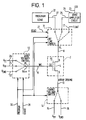
- Figure 1 illustrates a flash memory cell 2 comprising a single floating gate transistor 4 having a control gate CG , a floating gate FG , a source S , and a drain D .
- the source S of the floating gate transistor 4 is connected to an ARRAY GROUND signal on line 10.
- this line 10 can be at a ground voltage VGND or a high voltage Vpp .
- Voltage Vpp represents a programming potential (typically 12V) and voltage VGND represents device ground.
- Vpp is normally connected to array ground, either directly or via a resistor (not shown).
- the source voltage switch 14 is connected to the voltage Vpp via line 34 and the voltage VGND via line 36.
- the control gate CG of the floating gate transistor 4 is connected to the output voltage Vccx on line 29 of a gate voltage switch 12 by a word line ( WL ) 8.
- the gate voltage switch 12 is further connected to voltages Vcc , Vpp and VGND on lines 26, 24 and 22 respectively.
- Vcc is at 5V for a 5V part or 3V for a 3V part.
- These switches 14 and 12 each receive a control signal ERASE on line 28 and additionally the gate voltage switch 12 receives a control signal PROGRAM on line 30.
- the drain D of the floating gate transistor 4 is connected to a bit line switch 31 by a bit line ( BL ) 6.
- the switch 31 receives a control signal READ on line 21 in addition to the control signals PROGRAM and ERASE on lines 30 and 28 respectively.
- the flash memory has three primary modes of operation: program, erase and read. Each of these modes will be described hereinafter with reference to Figure 1. It will be understood by a person skilled in the art that several other modes of operation, such as program verify for example, also exist. However, the present description is by way of background illustration only, and therefore only these three modes will be described.
- the program mode involves writing a "0" to a memory cell or group of memory cells
- the erase mode involves removing a "0" from any cell that has a "0” stored in it such that the cells all effectively store “1”s
- the read mode involves reading a cell to establish whether it is programmed or erased, i.e. contains either a "0" or a "1".
- the control signal PROGRAM on line 30 is set such that the gate voltage switch 12 is configured to connect the voltage Vpp on line 24 to the control gate CG of transistor 4 via word line 8.
- the source voltage switch 14 is configured to connect the voltage VGND on line 36 to the source of transistor 4 via the ARRAY GROUND signal line 10.
- the bit line switch 31 is set such that the bit line on line 6 is connected to the program load 32 by line 27.
- the program load is such that a voltage of between 4 and 8V is on the drain D of the transistor 4 via the bit line 6.
- the negative charge increases the threshold voltage of the floating gate transistor making it less conductive.
- the amount of negative charge accumulated at the floating gate depends on several factors, including the duration for which the control signal PROGRAM is set, the voltages applied to the gate and drain terminals, and the thickness of the oxide separating the floating gate from the channel of the transistor. Furthermore, as the cell is programmed the accumulation of negative charge on the floating gate causes the electric field across the field oxide to reduce such that a point is reached where no more negative charge is attracted to the floating gate such that the threshold voltage of the floating gate transistor saturates to a limit. In this way, a "0" is written into the cell. Normally, several program pulses may be needed, each pulse being followed by a verify cycle.
- the control signal ERASE on line 28 is set such that the gate voltage switch 12 is configured to connect the voltage VGND on line 22 to the control gate CG of the transistor 4 via the word line 8, and such that the switch 14 is configured to connect the voltage Vpp on line 34 to the source S of the transistor 4 via the ARRAY GROUND line 10.
- the bit line switch 31 is set such that the bit line 6 is connected to the floating connection FLOAT on line 17 so that it floats. As the floating gate transistor is fabricated such that the source region in the substrate underlies the floating gate, any negative charge on the floating gate will be reduced. The amount of negative charge removed from the floating gate FG depends on the various factors as discussed above with reference to the program operation. The reduction of negative charge reduces the threshold voltage of the floating gate transistor making it more conductive. In this way the state of the cell is restored to "1". Normally, several erase pulses may be required, each erase pulse being followed by a verify cycle.
- the Vcc signal on line 26 is connected by the source voltage switch 12 to the control gate of the transistor 4 via the line Vccx and the word line 8. If the device is a 3V part, the supply voltage Vcc is disconnected from the signal Vccx , and hence the wordline WL 8 , is boosted above Vcc by means not shown.
- the voltage VGND on line 36 is connected to the source of the transistor 4 via the ARRAY GROUND signal line 10.
- the bit line 6 is biased to approximately 1 volt during a read operation by a bit line load within the sense amplifying circuit.
- Figure 2 illustrates a flash memory array 50 comprising a plurality of flash memory cells FMoo ... FMnm, arranged in rows and columns, each of which can be the same as the cell 2 shown in Figure 1.
- the gates of the transistors in each memory cell in a row are commonly connected to a respective word line WLo ... WLn addressable by a row line decode circuit 56 which receives the row address 64.
- the gate voltage switch 12 responds to the control signals PROGRAM and ERASE on line 30 and 28 respectively, and supplies the appropriate gate voltage Vccx on line 29 to be switched to the addressed wordline through the row decode circuit 56.
- the drains of each transistor in a column are commonly connected by bit lines BLo ... BLm to a column line decode circuit 58.
- the outputs of the bit line switches 57 on line 25 is a read output and is connected to the sense amplifier circuit 29.
- the sense amplifier circuit 29 contains a plurality of sense amplifiers (eight in the described embodiment to allow eight bits to be read in a common cycle), and hence the output on line 25 is actually a plurality of bits wide (eight in the described example).
- the bit line switches receive a write input on line 27 from the program load 32. During a program operation eight of the bit lines BLo to BLm are selectively connected to the program load 32.
- the program load 32 similarly comprises a plurality (in this example eight) of program loads, and hence the input on line 27 is actually also eight bits wide.
- the selected bit line (or bit lines) are connected to the sense amplifier circuit 29.
- the sense amplifier circuit 29 also receives a reference signal REF on line 72 and generates output signals on the data bus ( DB ) 23, which is an eight bit bus in the described embodiment.
- the respective output signals are generated by comparing the signals on the respective bitlines with the reference signal REF .
- a memory device which is compatible with both 3V and 5V supplies will require some means for determining which supply is being used.
- the boost circuitry described hereinafter will only be enabled when the supply is 3V.
- the device can be configured to match the available supply by means of a user input or by means of a detection circuit on the device which generates an appropriate signal on detection of a 3V or a 5V supply.
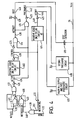
- Figure 4 illustrates diagrammatically a circuit (which may be used with the memory described hereinabove with reference to Figures 1 to 3) for providing the boosted voltage for the wordline for a device having only a low supply voltage.
- the circuitry includes a flip-flop 400 having a set-input S , a reset input R , and an output Q , the Q output being responsive to low going pulses on the set input S or the reset input R .
- the circuitry further includes two positive edge only delay circuits 402 and 404, each having an input and an output and having independent delays dl and d2 respectively, a main Vcc supply and first precharge circuit 406, a second precharge circuit 408, a boot capacitor 410, four two-input NAND gates 412 to 418, and a plurality of inverters 420..428.
- the flip-flop 400 receives at its set input S a signal NOTATD on line 430 which is the output signal from the address transition detection circuitry which indicates that transition has occurred to the address of a cell in the array.
- the address transition detection circuitry detects a transition on the address lines by generating a low going pulse on the signal NOTATD or a transition on the chip enable input by releasing the signal NOTATD from a low state.
- the reset input R of the flip-flop 400 receives a signal NOTRESET on line 448.
- the NAND gate 412 receives as one of its inputs the signal NOTATD on line 430 and as its other input the signal on the output Q of the flip-flop 400.
- the NAND gate 412 generates an output signal ACTIVE on line 434 via the inverter 421.
- the positive edge only delay circuit 402 receives as its input the signal ACTIVE on line 434.
- the inverter 424 receives as its input the output of the positive edge only delay dl circuit 402 and generates a signal CONTROL on its output on line 436.
- the inverter 426 receives as its input the signal CONTROL on line 436.
- the NAND gate 414 receives as one of its inputs the output of the inverter 426, and as the other of its inputs the signal ACTIVE on line 434.
- the output of the NAND gate 414 forms a signal NOTBOOT on line 438.
- the inverter 428 receives as its input the signal NOTBOOT on line 438 and generates at its output the signal BOOT on line 446.
- the inverter 428 selectively supplies the supply voltage Vcc to the signal BOOT in dependence on the state of the signal NOTBOOT .
- the NAND gate 416 receives as one of its inputs the signal NOTBOOT on line 438 and as the other of its inputs the signal ACTIVE on line 434.
- the NAND gate 416 generates at its output the signal PRECHARGE on line 442 via the inverter 423.
- the inverter 422 receives as its input the signal CONTROL on line 436 and generates a signal NOTCONTROL on line 451.
- the NAND gate 418 receives as one of its inputs a signal FINISH on line 432 and as the other of its inputs the signal NOTCONTROL on line 451.
- the output of the NAND gate 418 forms the signal NOTRESET on line 448.
- the positive edge only delay d2 circuit 404 recieves at its input the signal CONTROL on line 436, and the inverter 420 receives as its input the ouput of the positive edge only delay d2 circuit 404 and generates a signal VCCOFF at its output on line 444.
- the main Vcc supply and first precharge circuit 406 receives the supply voltage Vcc and the signal VCCOFF on line 444 and is also connected to the signal Vccx on line 29. During a read cycle the supply voltage Vcc is selectively connected to the signal Vccx by the main Vcc supply and first precharge circuit under control of the signal VCCOFF .
- the second precharge circuit 408 receives the supply voltage Vcc and the signal PRECHARGE on line 442 and is also connected to the signal Vccx on line 29. The supply voltage Vcc is selectively connected to the signal Vccx by the second precharge circuit under control of the signal PRECHARGE .
- the boot capacitor 410 has one terminal connected to the signal BOOT on line 446, and its other terminal connected to the signal Vccx on line 29.
- the signal on the output of the address transition detection circuitry is a negative going pulse. This signal goes low on detection of an address transition and remains low for a fixed period determined by the address transition detection circuitry. Should any further address transistions be detected then the output of the address transition circuitry will remain low until the address lines or other lines monitored by the address transition detection circuitry have stabilised. A positive going edge of the signal NOTATD on line 430 starts the boost cycle.
- the flip-flop 400 is a set-reset flip-flop responsive to low going pulses. That is to say, the output Q of the flip-flop changes state in response to low going pulses on one of its inputs S or R . A low going pulse on the set input S sets the output Q high, and the output Q remains in this state until a low going pulse on the reset input R resets the output Q low. In the event of simultaneous low going pulses on the set input S and the reset input R , Q will be forced high.
- the flip-flop 400 comprises two NAND gates 401 and 403.
- the NAND gate 401 receives as one input the signal NOTATD on line 430 via the set input S of the flip-flop 400, and as its other input the output of the NAND gate 403.
- the output of the NAND gate 401 forms the Q output of the flip-flop 400.
- the NAND gate 403 receives as one input the signal NOTRESET via the reset input R of the flip-flop 400, and as its other input the output of the NAND gate 401
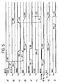
- the signal NOTATD on line 430 transitions from high to low as represented by edge 800 of Figure 5(a).
- the output Q of the flip-flop 400 is set high.
- the signal ACTIVE on line 434 remains low due to the action of the NAND gate 412 and the inverter 421.
- the signal NOTATD is held low for a fixed period d2 determined by a delay in the address transition detection circuitry, and then goes high, as represented by edge 802 of Figure 5(a).
- the signal ACTIVE goes high as shown by edge 804 of Figure 5(b).
- the signal ACTIVE going high represents the start of a boost cycle.
- the address transition detection circuitry may detect an address transition after a time when a read operation (and hence a boost operation) has already been initiated. In such a case the current read cycle must be aborted and a new one started. A more detailed explanation of such operation will be given later.
- a reset it is necessary for a reset to be performed before a further read or boost cycle can be performed.
- the duration of the reset is the delay d2 of the address transition detection circuitry.
- Such a reset is important to ensure that the wordline supply Vccx has returned to a known voltage level at the start of the boost operation. If a reset is not performed then the wordline supply may be further boosted.
- a programmed cell (the floating gate transistor associated therewith having a relatively high threshold voltage) may unnecessarily turn on and conduct current. Furthermore, boosting to an unnecessarily high voltage wastes power and would increase the time required to reset the wordline supply to the power supply. The period for which such a reset operation needs to be carried out is dependent upon how fast the wordline supply can be returned to the required known voltage, which will be dependent upon the capacitance of the wordline supply and the reset circuit.
- the circuitry used to reset the wordline supply is the same as that used to boost the wordline supply.
- the negative going pulse of the signal NOTATD has a width d2 determined by the length of the reset period required. It is stressed that the wordline supply is boosted from a well defined level (Vcc) and to a well defined level, dependent on the relative size of the boost capacitor and the capacitance of the wordline supply.
- the signal ACTIVE determines whether a read or boost cycle is active or not; when the signal ACTIVE is high a read or boost cycle is in progress. Forcing the signal ACTIVE low therefore resets a boost cycle.
- the signal ACTIVE is held low when the signal NOTATD is low. Therefore, the negative going pulse of the NOTATD signal can be conveniently used as a reset signal, and the address transition detection circuitry is configured such that on detection of an address transition the NOTATD signal is held low for the period d2 equal to the period required to reset the wordline supply to the required known level.
- the signal ACTIVE going high terminates the reset period.
- the signal ACTIVE prior to the negative going pulse of the signal NOTATD the signal ACTIVE was low and hence in this example the previous read cycle had completed, and was therefore not aborted by the new NOTATD pulse.
- the precharge period starts and the signal PRECHARGE on line 442 goes high as represented by edge 816 of Figure 5(e).
- the second precharge circuit 408 therefore becomes active and starts precharging the wordline signal level Vccx to the supply voltage Vcc .
- the main Vcc supply and first precharge circuit 406 has been active supplying the supply voltage Vcc to the wordline signal level Vccx .
- the main Vcc supply and first precharge circuit therefore has clamped the wordline supply Vccx to the supply voltage Vcc .
- the main Vcc supply and first precharge circuit 406 is only inactive during the time that the wordline supply Vccx is to be boosted above the supply voltage Vcc , and is otherwise active. Between an aborted cycle and a new cycle the main Vcc supply and first precharge circuit 406 is activated for the same time as the second precharge circuit 408 and hence acts as a source of precharge to Vccx during this time.
- the delay dl is determined by the positive edge only delay dl circuit 402.
- the signals PRECHARGE and VCCOFF change state as represented by edges 818 and 820 respectively.
- the delay dl of the positive edge only delay dl circuit 402 determines the precharge time of the boost cycle.
- the signals PRECHARGE and VCCOFF changing state will disable the second precharge circuit 408 and the main Vcc supply and first precharge circuit 406 respectively such that the line 29 carrying the signal Vccx becomes high impedence. This then terminates the precharge period of the cycle.
- the signal NOTBOOT on line 438 becomes active by going low.
- the signal BOOT on line 446 will start to rise towards Vcc as fast as possible. This is the start of the boost phase of the cycle.
- the rise of the signal BOOT is slowed by charging the heavy capacitive node BOOT .
- the speed of the edge 812 will be determined by the size of the drive inverter 428 and the size of the boot capacitor 410.
- the size of the boot capacitor 410 is determined by the amount of capacitance on the wordline supply connected to the signal Vccx .
- the wordline signal level Vccx rises from the level of the supply voltage Vcc to a fixed voltage V B above the supply voltage Vcc as illustrated by the edge 828 of Vccx , as a result of the coupling action of the boot capacitor 410. Once the wordline has been boosted the sensing operation can be initiated.
- a positive going pulse on the signal FINISH indicates the end of the sense operation so that the wordline signal level Vccx can now return to its quiescent level.
- the origin and generation of the signal FINISH will be discussed in detail later.
- a negative going pulse on the signal NOTRESET on line 448 resets the flip-flop 400 and the Q output goes low and hence the signal ACTIVE goes low.
- the signal VCCOFF remains high during the time that the signal Vccx returns to the supply voltage Vcc .
- the time at which the signal VCCOFF changes state in response to the signal CONTROL going high is determined by the positive edge delay d2 circuit 404. This delay is fixed to be the reset period d2, ie the time required for the wordline signal level Vccx to return to the known voltage level of the supply voltage Vcc .
- the signal VCCOFF goes low and the main Vcc supply and first precharge circuit 406 beomes active to provide the supply voltage Vcc to the wordline Vccx .
- the boost scheme according to the present example also has particular advantages when used in a memory device which uses at least one dynamic sense amplifier, and in particular in relation to generation of the signal FINISH .
- Dynamic sence amplifiers take many forms, but work on the common principle of developing a small differential signal on two input lines, this small differential signal being developed into full complementary CMOS signals on the output of the dynamic sense amplifier.
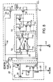
- FIG 6 there is shown an illustrative block diagram of a dynamic sense amplifier and associated circuitry such as may be used in a memory device.
- a dynamic sense amplifier 600 receives a differential input signal on lines 608 and 610 represented by signals INPUT1 and INPUT2 respectively.
- the differential signal may be a current or voltage differential signal.
- the amplifier is clocked or latched and a regenerative feedback action occurs within the sense amplifier such that latched full complementary signals appear as signals SAOUT and NOTSAOUT on lines 612 and 614 respectively.
- the signal which clocks the dynamic sense amplifier 600 is represented by a signal CLOCK on line 616.
- the outputs SAOUT and NOTSAOUT on lines 612 and 614 respectively form the inputs to a read bus driver 601.
- the read bus driver 601 generates complementary outputs READBUS and NOTREADBUS on signal lines 630 and 632 respectively.
- the signals READBUS and NOTREADBUS on lines 630 and 632 form inputs to a latch 602.
- the output of the latch 602 is a data output bit DB' on line 618 which forms an input to an output buffer 604.
- the data output bit DB' is one bit of the eight bit data bus DB.
- the output of the output buffer 604 is a signal OUT on line 620 which is presented on an output pad 606.
- the differential signals on the inputs to the dynamic sense amplifier can return to their default state because the outputs of the amplifier are latched in a stable state.
- the dynamic sense amplifier has been clocked such that the data to be read has been latched on its ouput the boosted signal can be removed from the wordline of the selected memory cell.
- the signals READBUS and NOTREADBUS on lines 630 and 632 also form the inputs to a two input NOR gate 634, which generates the signal FINISH on output line 432 via an inverter 638.
- the signals READBUS and NOTREADBUS Prior to a read cycle the signals READBUS and NOTREADBUS are precharged to zero volts by means not shown, but well understood by a person skilled in the art.
- the dynamic sense amplifier 600 is clocked by the signal CLOCK on line 616, the data on the outputs SAOUT and NOTSAOUT is propogated onto the signals READBUS and NOTREADBUS such that one of them will change from zero volts to a logical high state.
- the output of the NOR gate 634 will change from high to low and consequently the signal FINISH will change from low to high.
- the signal FINISH which ends the boost cycle is generated once the dynamic sense amplifier has settled into its stable state having driven its data onto the signals READBUS and NOTREADBUS .
- the signal FINISH could be derived directly from the signal CLOCK which clocks the dynamic sense amplifer 600.
- such a scheme would not be as advantageous as detecting a signal on the outputs of the read bus driver 601 if the dynamic sense amplifier was slow to settle and the logic path back to the flip-flop was fast, such that the cycle was terminated before the sense amplifier settled. In this case the output would be invalid.
- the scheme of the present example allows for the boost cycle to be ended asynchronously immediately a stable data value has been latched by the dynamic sense amplifier. Therefore, as soon as the data value has established the boost circuit can be reset ready for another read or boost cycle.
- Such an asynchronous operation for ending a boost cycle is advantageous since it means that no timer circuit is required for ending the boost cycle a fixed time after the start of the boost cycle.
- a signal to start a read cycle ie a negative going pulse on the signal NOTATD
- a signal to finish a read cycle ie a positive going pulse on the signal FINISH
- the signal to start the read cycle must take precedence over the signal to finish the read cycle.
- Such a precedence is achieved by applying the signal FINISH to the reset input R of the flip-flop 400 via the NAND gate 418.
- the negative going pulse on the signal NOTATD will force the signal CONTROL high such that the signal NOTCONTROL on the other input of the NAND gate 418 will be low, such that the output of the NAND gate 418 is forced high regardless of the signal FINISH .
- the Q output of the flip-flop 400 With the signal NOTATD low, the Q output of the flip-flop 400 will be high. After being set high, the signal CONTROL will remain high for a length of time determined by the delay dl of the positive edge only delay dl circuit. Therefore by the time the signal CONTROL returns low the signal FINISH will have returned low. In the example described above for generating the FINISH signal the signals READBUS and NOTREADBUS would return to their default state in this time such that the signal FINISH would return low. The circuit of Figure 4 will therefore now be guaranteed to be in a start of cycle state, and the new read cycle will commence normally. It can therefore be understood that a signal to finish a read cycle will only have an effect on the circuit of Figure 4 after the signal CONTROL has gone low.
- the signal CONTROL takes control of the read cycle; the read cycle is only allowed to finish if the signal CONTROL is low, since if the signal CONTROL is high either the read cycle has already finished or else the signal to finish the read cycle has occured too near the beginning of a new cycle.
- Figure 7 shows the signals on two address lines A2 (Figure 7(b)) and A3 ( Figure 7(c)) and the signal transitions on a chip enable signal NOTCE ( Figure 7(a)).
- the signal NOTATD on line 430 is held low by a chip enable buffer, and all the other signals of the circuit of Figure 4 are in their default states such that the reset signal NOTRESET on line 448 is high.
- the device In response to a chip enable signal NOTCE going from high to low the device, of which the circuitry of Figure 4 forms a part, becomes enabled.
- the signal NOTATD goes high as represented by edge 502.
- the signal NOTATD going high causes the signal ACTIVE to go high as represented by edge 504 of Figure 7(e), and hence a boost cycle commences as described previously with reference to Figure 5.
- the signal PRECHARGE goes high as illustrated by edge 510 of Figure 7(h), and consequently the second precharge circuit 408 turns on to precharge the signal Vccx to Vcc .
- the signal BOOT on line 446 returns to a low level and the signal Vccx returns to a level of approximately Vcc , as represented by edges 536 and 539 respectively.
- the signal VCCOFF goes low as illustrated by edge 538 and the main Vcc supply and first precharge circuit 406 starts supplying Vcc to the signal Vccx .
- the signal NOTATD remains low since transitions are still occurring on the address lines A2 and A3 .
- a succession of transitions are detected by the address transition detection circuit on the address signals A2 and A3 such that the signal NOTATD remains low for a long period.
- the address transition detection circuitry will not generate the trailing edge of the address transition pulse until the inputs being monitored have been stable for a fixed time. Consequently, some time after the start of the pulse on the signal NOTATD represented by falling edge 524, rising edge 544 indicates the end of the address transition detection pulse, propagated as edge 546 in the signal ACTIVE , and the circuit of Figure 4 is released to enter a boost cycle.
- the signal PRECHARGE on line 442 goes high as represented by edge 548 and hence the second precharge circuit 408 assists the main Vcc supply and first precharge circuit 406 in precharging the signal Vccx to the supply voltage Vcc . From this point onwards the circuit of Figure 4 operates in the same way as was described hereinabove with reference to the timing diagrams of Figure 5.
- the signal CONTROL on line 436 goes low on edge 552 in response to the positive edge 546 propogated through the positive edge only delay dl circuit 402.
- the signal NOTBOOT on line 438 goes low and the signal VCCOFF on line 444 goes high as shown by the edge 556.
- the signal PRECHARGE on line 442 goes low on edge 558 in response to the signal NOTBOOT going low.
- both the second precharge circuit 408 and the main Vcc supply and first precharge circuit 406 are disabled and the signal Vccx on line 29 becomes tristate.
- the signal BOOT on line 446 then starts to rise to the supply voltage Vcc as represented by edge 560, and consequently the signal Vccx will rise to a voltage V B above the supply voltage Vcc as represented by the edge 562. As before described, the signal Vccx will then remain in the boosted state until a further address transition pulse or until the signal FINISH on line 432 goes high.
- the timing sequence of the signal FINISH is shown in Figure 7(m).
- the signal CONTROL goes high as illustrated by the positive edge 570, and further consequently the signal NOTBOOT goes high.
- the signal BOOT on line 446 goes low as illustrated by negative edge 574 and consequently the signal Vccx goes towards the supply voltage Vcc as illustrated by negative edge 576.
- a fixed period d2 (determined by the delay of the positive edge only delay d2 circuit 404) after the positive edge 570 of the signal CONTROL the reset period is terminated by a negative edge 578 of the signal VCCOFF , and hence the signal Vccx is precharged to the supply voltage Vcc .
- the FINISH signal on line 432 goes low as shown by edge 580 because the READBUS and NOTREADBUS signals are precharged low by means not shown but under the control of the circuit of Figure 4.
- the boost scheme provided by the present invention has three distinct phases namely reset, precharge and boost.
- the reset phase causes the signal Vccx to be reset to a level of approximately the supply voltage. It is important to boost from a well-defined level in order to boost to a well-defined level, and the reset and precharge operations are important to this condition. It is important that with successive boost operations that neither 'walk-down' occurs (since cell currents may become too small for sensing) or 'walk-up' occurs, since this is unnecessary and may stress devices attached to the boosted node.
- the size of the fixed voltage V B above which the signal Vccx is boosted is dependent upon the characteristics of the boot capacitor 410. Hence the reset and precharge phases ensure that the signal Vccx is always returned to a known level.
- the precharge phase precharges the signal Vccx to the supply voltage Vcc .
- precharge is provided by two circuits: the main Vcc supply and first precharge circuit 406 and the second precharge circuit 408.
- precharge is only supplied by a single precharge circuit separate to the circuit providing the main Vcc supply.
- the circuit supplying the main Vcc supply cannot generally be used for providing precharge because of the physical size of the devices it requires.
- Such a circuit requires large p-type transistors because of the need to provide Vcc from a low impedance supply.
- the circuit supplying the main Vcc supply cannot generally be used for providing precharge because the switching speed of such circuits is inherently slow.
- a precharge circuit to be used in a boost scheme such as that provided by the present example needs to be able to switch on and off quickly to minimise the length of the precharge period.
- a separate precharge circuit capable of fast switching is conventionally provided, typically comprising of p-type transistors.
- a circuit for supplying the main Vcc supply which is capable of switching rapidly and can therefore also be used to provide precharge during a boost cycle.
- the circuit for supplying the main Vcc supply is conventionally comprised of p-type transistors such a circuit will provide p-type precharge.
- the main Vcc supply and first precharge circuit 406 provides precharge through p-type devices and the second precharge circuit 408 provides precharge through n-type devices.
- the second precharge circuit 408 provides precharge through n-type devices.
- the signal Vccx becomes tristate, and is then boosted to a voltage above the supply voltage Vcc .
- the second precharge circuit 408 comprises a capacitor 450 and four n-channel transistors 700, 702, 703 and 704.
- the capacitor 450 has one terminal connected to the signal PRECHARGE on line 442, and another terminal to a line 452 which forms a signal NDRIVE .
- the transistor 700 has its gate connected to the signal Vccx on line 29, its drain connected to the supply voltage Vcc , and its source connected to the signal NDRIVE on line 452.
- the transistor 702 has both its gate and its drain connected to the supply voltage Vcc , and its source connected to the signal NDRIVE on line 452.
- the transistor 704 has its drain connected to the supply voltage Vcc, its gate connected to the signal NDRIVE on line 452, and its source connected to the signal Vccx on line 29.
- the transistor 703 has both its gate and its drain connected to the supply voltage Vcc, and its source connected to the signal Vccx .
- the main Vcc supply and first precharge circuit 406 comprises an elevator circuit 750 consisting of an inverter 706, two p-channel transistors 710 and 712 and two n-channel transistors 722 to 724; a NAND gate 752 comprising two p-channel transistors 714, 716 and two n-channel transistors 726 and 728; in addition to two inverters 708, 709, two p-channel and a bias circuit 730.
- P-channel transistor 710 has its source connected to the signal Vccx on line 29, its well connected to its source, its gate connected to a signal ENPRE on line 732, and its drain connected to the drain of the n-channel transistor 722.
- the transistor 722 has its source connected to the negative supply voltage or ground Vss and its gate connected to a signal VCCCONTROL on line 701.
- the p-channel transistor 712 has its source connected to the signal Vccx on line 26, its well connected to its source, its gate connected to the drain of the n-channel transistor 722, and its drain connected to the signal ENPRE on line 732.
- the n-channel transistor 724 has its drain connected to the signal ENPRE on line 732, its source connected to the negative supply voltage or ground Vss , and its gate connected to the inverse of the signal VCCCONTROL on line 701 via the inverter 706.
- the p-channel transistor 714 has its source connected to signal Vccx on line 29, its well connected to its source, its gate connected to the signal ENPRE on line 732, and its drain connected to the drain of the n-channel transistor 726.
- the n-channel transistor 726 further has its gate connected to the signal ENPRE on line 732 and its source connected to the drain of the n-channel transistor 728.
- the n-channel transistor 728 further has its gate connected to the inverse of the signal VCCOFF on line 444 via the inverter 708, and its source connected to the negative supply voltage or ground Vss.
- the p-channel transistor 716 has its source connected to the signal Vccx on line 29, its well connected to its source, its gate connected to the inverse of the signal VCCOFF on line 444 via the inverter 708, and its drain connected to the common drain connection of the transistors 714 and 726.
- the p-channel transistor 718 has its source connected to the supply voltage Vcc , its gate connected to the inverse of the signal VCCCONTROL on line 701 via the inverter 709, and its drain connected to the drain of the p-channel transistor 720.
- the p-channel transistor 720 has its gate connected to the common drains of transistors 714 and 726 and its source connected to the signal Vccx on line 29.
- the bias circuit 730 is connected to the common drains of the transistors 718 and 720.
- the transistor 702 serves to bias the signal NDRIVE 452 at a voltage equal to the supply voltage Vcc less the threshold voltage V TN of the transistor 702. Therefore, as the supply voltage Vcc rises from zero to its final value, the signal NDRIVE rises from zero such that its instantaneous value is V CC -V TN .
- the diode connected transistor 703 serves to bias the signal Vccx to V CC -V TN .
- the transistor 702 holds the signal NDRIVE at V CC -V TN , and transistor 703 pulls Vccx up to V CC -V TN . Otherwise during power-up the level of Vccx could not be guaranteed.
- the voltage level on Vccx guaranteed by the operation of the second precharge circuit 408, ensures there is sufficient voltage to power any logic circuits required to be powered by Vccx during power-up, for example wordline drivers.
- the main Vcc supply and first precharge circuit 406 ensures the signal Vccx is at Vcc , and therefore the transistor 700 ensures that the signal NDRIVE on line 452 is maintained at a voltage of Vcc-V TN .
- the signal PRECHARGE on line 442 is equal to zero volts.
- the signal NDRIVE on line 452 must be taken well above the level of Vcc, and this is achieved by the use of the capacitor 450.
- the signal PRECHARGE on line 442 will go high.
- the signal PRECHARGE going high will cause the signal level at the node NDRIVE to rise due to the coupling action of the capacitor 450.
- the transistor 700 is used to hold NDRIVE at a default level of V cc -V TN once power-up has been completed.
- the main Vcc supply and first precharge circuit 408 has two roles. Its primary role is to provide the supply voltage Vcc to the wordline via the signal Vccx , and its secondary role is to precharge the signal Vccx to Vcc during the precharge phase of a boost cycle for devices which have a low supply voltage. It should therefore be apparent that in devices which have a supply voltage Vcc of 5V the secondary function of the main Vcc supply and first precharge circuit is never utilised. Hence, during normal operation of the main Vcc supply and first precharge circuit 406, the circuit merely operates to provide the supply voltage Vcc to the wordline via the signal Vccx , by means of the p-channel transistors 718 and 720.
- the signal VCCCONTROL is normally high such that the p-channel transistor 718 is normally on.
- the signal VCCOFF is normally low.
- the signal VCCOFF is low, the transistor 728 is on, and the transistor 716 is off.
- the signal VCCCONTROL ensures that the transistor 722 is on and the transistor 724 is off.
- the transistor 712 is on such that the signal level on Vccx appears as the signal ENPRE .
- Vccx is at a high signal level (either as a result of the action of the second precharge circuit 408 or the main Vcc supply and first precharge circuit 406), the signal ENPRE will be high.
- the signal ENPRE is inverted by the NAND gate effectively formed by the transistors 714, 716, 726 and 728 such that the signal on the gate of the p-channel transistor 720 is low and hence the transistor 720 is on. In this way the signals VCCCONTROL and VCCOFF ensure that the signal Vccx is precharged to Vcc through the transistors 718 and 720.
- the transistor 716 ensures that the gate of the transistor 720 is connected to the signal line Vccx , which immediately prior to the boost will be Vcc . Hence the transistor 720 turns off and the line Vccx becomes tristate. As the voltage level on the line Vccx rises above Vcc the voltage level on the gate of transistor 720 will follow it. It is essential that the gate of the transistor 720 is taken to the boosted voltage level. If the gate of the transistor 720 was merely held at Vcc , while its drain was connected to the boosted voltage on Vccx , the transistor 720 would not be fully turned off and there would be a path from Vcc to Vccx which would degrade the boost operation.
- the second precharge circuit 408 has no effect on the signal level on Vccx since all the transistors that are connected to the wordline via Vccx in the precharge circuit are n-channel.
- the elevator circuit 750 does not switch very quickly because the n-channel transistors 722 and 724 must turn on or off before the dc levels are established on the output nodes ENPRE and NOTENPRE , and feedback action via the cross-couple arrangement takes place before the p-channel devices turn on or off, unlike a normal CMOS switching device where the n-channel devices and the p-channel devices switch simultaneously. If the device 720 cannot be turned on and off quickly, then the main Vcc supply and first precharge circuit 406 cannot be used also as a precharge circuit during aborted read cycles.
- the transistors 714, 716, 726 and 728, forming the NAND gate 752 have been added to the conventional elevator control of the main Vcc supply circuit.
- This arrangement acts as a buffer so that the transistors 710, 712, 722, 724 and the inverter 706 can be made much smaller.
- the VCCOFF signal is then directly gated into the NAND arrangement in order to obtain the necessary fast switching speed.
- the switching of the p-channel transistor is now controlled by the NAND gate 752, and in turn the switching of the NAND gate during a read cycle is controlled only by the signal VCCOFF (the signal VCCCONTROL and hence the signal ENPRE remaining in the same state during a boost cycle).
- VCCOFF the signal VCCCONTROL and hence the signal ENPRE remaining in the same state during a boost cycle.
- the inverse of the signal VCCOFF switches both the n-channel device 728 and the p-channel device 716 of the NAND gate simultaneously, thus providing the necessary fast switching.
- the CMOS input from the inverse of the signal VCCOFF to the NAND gate is acceptable because the voltage on the gate of p-channel transistor 716 is only high when either the signal Vccx is equal to Vcc as in a read cycle, or when Vccx is driven by some other source, eg a 12V supply for a program operation.
- the signal VCCCONTROL is low and hence the signal ENPRE is low, and therefore the p-channel transistor 714 is on ensuring the gate of the p-channel transistor 720 is high. For this reason it is acceptable to have a CMOS input to the NAND gate with a variable level supply (ie Vccx ) as in this instance.
Landscapes
- Engineering & Computer Science (AREA)
- Microelectronics & Electronic Packaging (AREA)
- Physics & Mathematics (AREA)
- Nonlinear Science (AREA)
- Electromagnetism (AREA)
- General Physics & Mathematics (AREA)
- Radar, Positioning & Navigation (AREA)
- Automation & Control Theory (AREA)
- Read Only Memory (AREA)
- Static Random-Access Memory (AREA)
Applications Claiming Priority (2)
| Application Number | Priority Date | Filing Date | Title |
|---|---|---|---|
| GB9423035 | 1994-11-15 | ||
| GB9423035A GB9423035D0 (en) | 1994-11-15 | 1994-11-15 | Voltage boost circuit for a memory device |
Publications (1)
| Publication Number | Publication Date |
|---|---|
| EP0713165A1 true EP0713165A1 (de) | 1996-05-22 |
Family
ID=10764429
Family Applications (1)
| Application Number | Title | Priority Date | Filing Date |
|---|---|---|---|
| EP95308017A Withdrawn EP0713165A1 (de) | 1994-11-15 | 1995-11-09 | Spannungserhöhungsschaltung für Speichervorrichtung |
Country Status (4)
| Country | Link |
|---|---|
| US (1) | US5642313A (de) |
| EP (1) | EP0713165A1 (de) |
| JP (1) | JP2828616B2 (de) |
| GB (1) | GB9423035D0 (de) |
Cited By (1)
| Publication number | Priority date | Publication date | Assignee | Title |
|---|---|---|---|---|
| EP0864156A4 (de) * | 1996-10-01 | 2000-06-14 | Microchip Tech Inc | Lesen mit geschalteter erdung für eprom-speicherschaltung |
Families Citing this family (11)
| Publication number | Priority date | Publication date | Assignee | Title |
|---|---|---|---|---|
| KR0170286B1 (ko) * | 1995-12-22 | 1999-03-30 | 김광호 | 반도체 메모리장치의 전압 승압회로 |
| US5774405A (en) * | 1996-03-28 | 1998-06-30 | Mitsubishi Denki Kabushiki Kaisha | Dynamic random access memory having an internal circuit using a boosted potential |
| US5870573A (en) * | 1996-10-18 | 1999-02-09 | Hewlett-Packard Company | Transistor switch used to isolate bus devices and/or translate bus voltage levels |
| US5835410A (en) * | 1997-06-09 | 1998-11-10 | Microchip Technology Incorporated | Self timed precharge sense amplifier for a memory array |
| US6115295A (en) * | 1997-07-31 | 2000-09-05 | Texas Instruments Incorporated | Efficient back bias (VBB) detection and control scheme for low voltage DRAMS |
| US5847946A (en) * | 1997-12-15 | 1998-12-08 | Pericom Semiconductor Corp. | Voltage booster with pulsed initial charging and delayed capacitive boost using charge-pumped delay line |
| US5946204A (en) * | 1997-12-15 | 1999-08-31 | Pericom Semiconductor Corp. | Voltage booster with reduced Vpp current and self-timed control loop without pulse generator |
| JP2001216784A (ja) * | 2000-01-31 | 2001-08-10 | Mitsubishi Electric Corp | 半導体装置 |
| US6243316B1 (en) * | 2000-02-09 | 2001-06-05 | Advanced Micro Devices, Inc. | Voltage boost reset circuit for a flash memory |
| US6225849B1 (en) * | 2000-02-25 | 2001-05-01 | Advanced Micro Devices, Inc. | High speed, high precision, power supply and process independent boost level clamping technique |
| US10636470B2 (en) * | 2018-09-04 | 2020-04-28 | Micron Technology, Inc. | Source follower-based sensing scheme |
Citations (8)
| Publication number | Priority date | Publication date | Assignee | Title |
|---|---|---|---|---|
| US4639622A (en) * | 1984-11-19 | 1987-01-27 | International Business Machines Corporation | Boosting word-line clock circuit for semiconductor memory |
| US4704706A (en) * | 1985-04-13 | 1987-11-03 | Fujitsu Limited | Booster circuit |
| US4896297A (en) * | 1987-10-23 | 1990-01-23 | Mitsubishi Denki Kabushiki Kaisha | Circuit for generating a boosted signal for a word line |
| US4916334A (en) * | 1987-07-29 | 1990-04-10 | Kabushiki Kaisha Toshiba | High voltage booster circuit for use in EEPROMs |
| EP0367450A2 (de) * | 1988-10-31 | 1990-05-09 | Texas Instruments Incorporated | Verfahren und Ladungsfesthaltesignal-Erhöhungsschaltung |
| EP0505158A2 (de) * | 1991-03-18 | 1992-09-23 | Fujitsu Limited | Integrierte Halbleiterschaltung |
| US5258955A (en) * | 1990-09-25 | 1993-11-02 | Sgs-Thomson Microelectronics, S.A. | Pre-charging method for the reading of memories |
| EP0585150A1 (de) * | 1992-07-24 | 1994-03-02 | STMicroelectronics S.A. | Speicher-Leseschaltung mit Vorladung und Ausgleichung vor dem Lesen |
Family Cites Families (7)
| Publication number | Priority date | Publication date | Assignee | Title |
|---|---|---|---|---|
| JPS60201591A (ja) * | 1984-03-26 | 1985-10-12 | Hitachi Ltd | 半導体集積回路装置 |
| JPS6437797A (en) * | 1987-08-03 | 1989-02-08 | Oki Electric Ind Co Ltd | Eprom device |
| JPH0252860A (ja) * | 1988-05-25 | 1990-02-22 | Nippon Denso Co Ltd | コイル装置 |
| JPH04129089A (ja) * | 1990-09-19 | 1992-04-30 | Mitsubishi Electric Corp | ダイナミック型半導体記憶装置 |
| JPH05151789A (ja) * | 1991-11-29 | 1993-06-18 | Nec Corp | 電気的に書込・一括消去可能な不揮発性半導体記憶装置 |
| JPH0684354A (ja) * | 1992-05-26 | 1994-03-25 | Nec Corp | 行デコーダ回路 |
| US5293342A (en) * | 1992-12-17 | 1994-03-08 | Casper Stephen L | Wordline driver circuit having an automatic precharge circuit |
-
1994
- 1994-11-15 GB GB9423035A patent/GB9423035D0/en active Pending
-
1995
- 1995-11-09 EP EP95308017A patent/EP0713165A1/de not_active Withdrawn
- 1995-11-15 JP JP29678695A patent/JP2828616B2/ja not_active Expired - Lifetime
- 1995-11-15 US US08/558,326 patent/US5642313A/en not_active Expired - Lifetime
Patent Citations (8)
| Publication number | Priority date | Publication date | Assignee | Title |
|---|---|---|---|---|
| US4639622A (en) * | 1984-11-19 | 1987-01-27 | International Business Machines Corporation | Boosting word-line clock circuit for semiconductor memory |
| US4704706A (en) * | 1985-04-13 | 1987-11-03 | Fujitsu Limited | Booster circuit |
| US4916334A (en) * | 1987-07-29 | 1990-04-10 | Kabushiki Kaisha Toshiba | High voltage booster circuit for use in EEPROMs |
| US4896297A (en) * | 1987-10-23 | 1990-01-23 | Mitsubishi Denki Kabushiki Kaisha | Circuit for generating a boosted signal for a word line |
| EP0367450A2 (de) * | 1988-10-31 | 1990-05-09 | Texas Instruments Incorporated | Verfahren und Ladungsfesthaltesignal-Erhöhungsschaltung |
| US5258955A (en) * | 1990-09-25 | 1993-11-02 | Sgs-Thomson Microelectronics, S.A. | Pre-charging method for the reading of memories |
| EP0505158A2 (de) * | 1991-03-18 | 1992-09-23 | Fujitsu Limited | Integrierte Halbleiterschaltung |
| EP0585150A1 (de) * | 1992-07-24 | 1994-03-02 | STMicroelectronics S.A. | Speicher-Leseschaltung mit Vorladung und Ausgleichung vor dem Lesen |
Cited By (1)
| Publication number | Priority date | Publication date | Assignee | Title |
|---|---|---|---|---|
| EP0864156A4 (de) * | 1996-10-01 | 2000-06-14 | Microchip Tech Inc | Lesen mit geschalteter erdung für eprom-speicherschaltung |
Also Published As
| Publication number | Publication date |
|---|---|
| JPH08227592A (ja) | 1996-09-03 |
| JP2828616B2 (ja) | 1998-11-25 |
| US5642313A (en) | 1997-06-24 |
| GB9423035D0 (en) | 1995-01-04 |
Similar Documents
| Publication | Publication Date | Title |
|---|---|---|
| US6141262A (en) | Boosting circuit with boosted voltage limited | |
| EP0713222B1 (de) | Integrierte Speicherschaltungsanordnung | |
| EP0961290B1 (de) | Flash-Speicher mit besserer Löschbarkeit und dessen Schaltung | |
| US6219277B1 (en) | Device and method for the reading of EEPROM cells | |
| US6587375B2 (en) | Row decoder for a nonvolatile memory device | |
| KR100509135B1 (ko) | 비트선 프리차징 시간을 감소시킨 반도체 기억 장치 | |
| EP0664544B1 (de) | Spannungsreduzierung für nichtflüchtige Speicherzelle | |
| EP0211232B1 (de) | Halbleiterspeicher mit einem Leseverfahren in einem grossen Speisespannungsbereich | |
| JPS63274362A (ja) | オン・チツプ多重レベル電圧発生装置 | |
| US5642313A (en) | Voltage booster circuit for a memory device | |
| KR100578581B1 (ko) | 플래시 이이피롬 워드라인 드라이버 | |
| US20040184321A1 (en) | High voltage positive and negative two-phase discharge system and method for channel erase in flash memory devices | |
| JP4394835B2 (ja) | 低パワー集積回路用高速オンチップ電圧発生器 | |
| KR19990022544A (ko) | 음의 전압 스위칭회로 | |
| EP1054408A2 (de) | Halbleiterspeicheranordnung | |
| JPS63271798A (ja) | 消去可能なプログラマブル論理装置 | |
| EP0698888A1 (de) | Steuerung einer kapazitiven Last | |
| US5917354A (en) | Circuit for resetting output of positive/negative high voltage generating circuit to VCC/VSS | |
| JPH11134892A (ja) | 内部電位発生回路 | |
| JP3011570B2 (ja) | 半導体メモリ | |
| KR102328355B1 (ko) | 반도체 기억장치 및 프리차지 방법 | |
| CN117995229A (zh) | 灵敏放大电路及驱动电路、随机存储器 | |
| JP3204799B2 (ja) | 半導体メモリ装置 | |
| WO1999039351A1 (en) | A voltage regulator and boosting circuit for reading a memory cell at low voltage levels | |
| JP2596144B2 (ja) | 不揮発性半導体記憶装置 |
Legal Events
| Date | Code | Title | Description |
|---|---|---|---|
| PUAI | Public reference made under article 153(3) epc to a published international application that has entered the european phase |
Free format text: ORIGINAL CODE: 0009012 |
|
| AK | Designated contracting states |
Kind code of ref document: A1 Designated state(s): DE FR GB IT |
|
| 17P | Request for examination filed |
Effective date: 19961118 |
|
| RAP3 | Party data changed (applicant data changed or rights of an application transferred) |
Owner name: STMICROELECTRONICS LIMITED |
|
| 17Q | First examination report despatched |
Effective date: 19990823 |
|
| GRAG | Despatch of communication of intention to grant |
Free format text: ORIGINAL CODE: EPIDOS AGRA |
|
| GRAG | Despatch of communication of intention to grant |
Free format text: ORIGINAL CODE: EPIDOS AGRA |
|
| GRAH | Despatch of communication of intention to grant a patent |
Free format text: ORIGINAL CODE: EPIDOS IGRA |
|
| STAA | Information on the status of an ep patent application or granted ep patent |
Free format text: STATUS: THE APPLICATION IS DEEMED TO BE WITHDRAWN |
|
| 18D | Application deemed to be withdrawn |
Effective date: 20010922 |