EP0713233A2 - Agencement d'un relais avec un adaptateur à fiches et procédé pour la fabrication de cet agencement - Google Patents
Agencement d'un relais avec un adaptateur à fiches et procédé pour la fabrication de cet agencement Download PDFInfo
- Publication number
- EP0713233A2 EP0713233A2 EP95116492A EP95116492A EP0713233A2 EP 0713233 A2 EP0713233 A2 EP 0713233A2 EP 95116492 A EP95116492 A EP 95116492A EP 95116492 A EP95116492 A EP 95116492A EP 0713233 A2 EP0713233 A2 EP 0713233A2
- Authority
- EP
- European Patent Office
- Prior art keywords
- base
- relay
- conductor segments
- peripheral wall
- arrangement
- Prior art date
- Legal status (The legal status is an assumption and is not a legal conclusion. Google has not performed a legal analysis and makes no representation as to the accuracy of the status listed.)
- Granted
Links
- 238000004519 manufacturing process Methods 0.000 title claims description 5
- 239000004020 conductor Substances 0.000 claims abstract description 31
- 150000001875 compounds Chemical class 0.000 claims abstract description 21
- 230000002093 peripheral effect Effects 0.000 claims abstract description 21
- 238000004382 potting Methods 0.000 claims abstract description 19
- 229910000679 solder Inorganic materials 0.000 claims abstract description 10
- 238000000034 method Methods 0.000 claims description 10
- 238000005476 soldering Methods 0.000 claims description 10
- 239000000463 material Substances 0.000 claims description 5
- 238000005266 casting Methods 0.000 claims description 4
- 238000007789 sealing Methods 0.000 claims description 4
- 239000011810 insulating material Substances 0.000 claims 2
- 238000003780 insertion Methods 0.000 abstract description 3
- 230000037431 insertion Effects 0.000 abstract description 3
- NFLLKCVHYJRNRH-UHFFFAOYSA-N 8-chloro-1,3-dimethyl-7H-purine-2,6-dione 2-(diphenylmethyl)oxy-N,N-dimethylethanamine Chemical compound O=C1N(C)C(=O)N(C)C2=C1NC(Cl)=N2.C=1C=CC=CC=1C(OCCN(C)C)C1=CC=CC=C1 NFLLKCVHYJRNRH-UHFFFAOYSA-N 0.000 description 1
- 238000007765 extrusion coating Methods 0.000 description 1
- 238000007654 immersion Methods 0.000 description 1
- 238000002347 injection Methods 0.000 description 1
- 239000007924 injection Substances 0.000 description 1
- 230000013011 mating Effects 0.000 description 1
- 239000002184 metal Substances 0.000 description 1
- 238000010791 quenching Methods 0.000 description 1
- 239000011347 resin Substances 0.000 description 1
- 229920005989 resin Polymers 0.000 description 1
- 238000000926 separation method Methods 0.000 description 1
- 230000006641 stabilisation Effects 0.000 description 1
- 238000011105 stabilization Methods 0.000 description 1
- 238000003466 welding Methods 0.000 description 1
Images


Classifications
-
- H—ELECTRICITY
- H01—ELECTRIC ELEMENTS
- H01H—ELECTRIC SWITCHES; RELAYS; SELECTORS; EMERGENCY PROTECTIVE DEVICES
- H01H50/00—Details of electromagnetic relays
- H01H50/02—Bases; Casings; Covers
- H01H50/04—Mounting complete relay or separate parts of relay on a base or inside a case
- H01H50/047—Details concerning mounting a relays
- H01H50/048—Plug-in mounting or sockets
-
- H—ELECTRICITY
- H01—ELECTRIC ELEMENTS
- H01R—ELECTRICALLY-CONDUCTIVE CONNECTIONS; STRUCTURAL ASSOCIATIONS OF A PLURALITY OF MUTUALLY-INSULATED ELECTRICAL CONNECTING ELEMENTS; COUPLING DEVICES; CURRENT COLLECTORS
- H01R13/00—Details of coupling devices of the kinds covered by groups H01R12/70 or H01R24/00 - H01R33/00
- H01R13/66—Structural association with built-in electrical component
- H01R13/6608—Structural association with built-in electrical component with built-in single component
-
- H—ELECTRICITY
- H01—ELECTRIC ELEMENTS
- H01R—ELECTRICALLY-CONDUCTIVE CONNECTIONS; STRUCTURAL ASSOCIATIONS OF A PLURALITY OF MUTUALLY-INSULATED ELECTRICAL CONNECTING ELEMENTS; COUPLING DEVICES; CURRENT COLLECTORS
- H01R31/00—Coupling parts supported only by co-operation with counterpart
- H01R31/06—Intermediate parts for linking two coupling parts, e.g. adapter
-
- H—ELECTRICITY
- H01—ELECTRIC ELEMENTS
- H01H—ELECTRIC SWITCHES; RELAYS; SELECTORS; EMERGENCY PROTECTIVE DEVICES
- H01H50/00—Details of electromagnetic relays
- H01H50/02—Bases; Casings; Covers
- H01H50/021—Bases; Casings; Covers structurally combining a relay and an electronic component, e.g. varistor, RC circuit
-
- H—ELECTRICITY
- H01—ELECTRIC ELEMENTS
- H01R—ELECTRICALLY-CONDUCTIVE CONNECTIONS; STRUCTURAL ASSOCIATIONS OF A PLURALITY OF MUTUALLY-INSULATED ELECTRICAL CONNECTING ELEMENTS; COUPLING DEVICES; CURRENT COLLECTORS
- H01R13/00—Details of coupling devices of the kinds covered by groups H01R12/70 or H01R24/00 - H01R33/00
- H01R13/46—Bases; Cases
- H01R13/52—Dustproof, splashproof, drip-proof, waterproof, or flameproof cases
- H01R13/5216—Dustproof, splashproof, drip-proof, waterproof, or flameproof cases characterised by the sealing material, e.g. gels or resins
-
- H—ELECTRICITY
- H01—ELECTRIC ELEMENTS
- H01R—ELECTRICALLY-CONDUCTIVE CONNECTIONS; STRUCTURAL ASSOCIATIONS OF A PLURALITY OF MUTUALLY-INSULATED ELECTRICAL CONNECTING ELEMENTS; COUPLING DEVICES; CURRENT COLLECTORS
- H01R13/00—Details of coupling devices of the kinds covered by groups H01R12/70 or H01R24/00 - H01R33/00
- H01R13/66—Structural association with built-in electrical component
- H01R13/6608—Structural association with built-in electrical component with built-in single component
- H01R13/6616—Structural association with built-in electrical component with built-in single component with resistor
Definitions
- the invention relates to the arrangement of a relay with connection pins emerging to a bottom side and a plug adapter lying below the bottom side, the adapter having an insulating base in which conductor segments of a lead frame are fastened in a plane parallel to the bottom side, the conductor segments each making contact Recesses for cohesive contacting, in particular solder contacting, of the connecting pins and also each have connecting lugs bent in one piece perpendicular to the bottom side.
- the invention also relates to a method for producing such an arrangement.
- connection elements of relays are designed in accordance with the intended use, that is, either as solder pins for directly soldering the relay into a printed circuit board or as flat plugs for plug-in contacting in a socket.
- Sockets have been known for a long time, which are soldered into a printed circuit board by means of soldering pins and have plug sockets on their upper side for receiving a pluggable relay.
- the aim of the present invention is therefore to convert a soldering relay into a plug-in arrangement, this arrangement being achievable with as little assembly effort as possible and having the smallest possible dimensions.
- plug connections for carrying high currents should be used, and a high stability of the combined arrangement should also be able to withstand high plug-in forces.
- this object is achieved with an arrangement of a relay and an adapter of the type mentioned at the outset in that the connecting lugs of the adapter are designed as flat plugs that both the space between the bottom side of the relay and the base and the outlet region of the flat plugs on the underside of the base are enclosed by a peripheral wall and that at least the latter area is filled with potting compound.
- flat plugs are provided from the outset in the arrangement according to the invention, that is to say so-called Faston or Quick Connect plugs, which are already used because of the occurring Mating forces require a corresponding material cross-section and can also carry high currents with this cross-section.
- the base itself is enclosed on its upper side facing the relay and on its lower side by a peripheral wall, so that the outlet area of the flat plugs, whose conductor segments can be anchored in the base by plugging in or embedding, is not only sealed by an additional potting, but also is stabilized.
- the entire adapter arrangement with the integrally soldered or welded relay thus results in a uniformly compact new part which is easy to handle and is suitable for use even with high insertion forces.
- the peripheral wall of the base can be integrally formed on it, so that it is trough-shaped both on the top and on the bottom. In this case, it is appropriate that the upper edge of the peripheral wall overlaps the lower edge of a housing cap of the relay.
- the space between the relay and base including the overlap gap can also be filled with potting compound, which gives the entire arrangement additional stability. In this case, the relay itself must be closed so far beforehand that the sealing compound cannot run into the interior of the relay. But it is also possible to design the peripheral wall on the base as an extension of a relay cap, so that the gap between the extended relay cap and the base is sealed by casting the underside of the base. The space between the relay and base is automatically sealed; but in this case it can also be filled with casting compound for stabilization.
- the tabs it is also possible in another embodiment of the invention to allow the tabs to run upwards from their point of exit from the base - on the underside or on the circumferential side of the base, perpendicular to the base plane, so that they run along one or more outer sides of the relay extend up to and beyond the relay top, whereby this relay top side then becomes the plug connection side of the overall arrangement, that is to say the relay is upside down.
- the tabs it is expedient for the tabs to be fixed on the outside of the relay by means of an overlaid frame-shaped sleeve and to be insulated from the outside. This sleeve can then also form the peripheral wall for the base and a trough-shaped receiving space for the sealing compound.
- An advantageous method for producing an arrangement according to the invention is that a lead frame with preformed conductor segments connected via intermediate webs and with likewise preformed flat plugs in a base is pre-fixed - by plugging in or embedding - that the intermediate webs are then separated out so that a relay is also used Connection pins are placed on the base and the connection pins are integrally connected, preferably soldered, to the conductor segments, and finally a cavity enclosed by a peripheral wall in the region of the base is filled with potting compound. It would also be conceivable to embed previously separate conductor segments in the base material instead of a one-part or two-part lead frame with intermediate webs, but this would require additional effort for holding the individual parts in the injection mold.
- this type of embedding would have the advantage that no separating processes for intermediate webs would be required on the finished base and that the finished base would have no other openings apart from the contact recesses; that would be an advantage if, for example, the relay itself on the underside were not closed and the flow of Potting compound in the gap to the relay should be prevented.
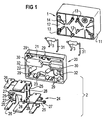
- the arrangement shown in Figures 1 to 4 comprises a relay 1 and a plug adapter 2, which are connected together.
- the relay 1 has a housing with a housing cap 11 attached from above and a base plate 12 forming the bottom side of the relay, through which solder pins 13 exit vertically downwards.
- the bottom side of the relay is sealed with casting resin via a channel or rib system 14.
- the adapter 2 comprises a base 20 with a base plate 21, on which a circumferential, up and down protruding peripheral wall 22 is formed.
- the peripheral wall 22 forms a cavity 23 which is open towards the underside and into which a lead frame 24 with a plurality of preformed conductor segments 25 and flat plugs 26 bent downwards is inserted.
- Each conductor segment 25 has at least one soldering recess 27 for inserting and soldering a connector pin 13 from relay 1 or from an additional component, and each conductor segment 25 is also connected in one piece to a flat plug 26.
- These flat plugs can have different widths, depending on whether they are required for carrying load current or only for carrying a smaller coil current.
- the base 20 is first equipped with the one-piece lead frame 24, so that the tabs 26 are pre-fixed to the holding ribs 29 mentioned. This state is shown in FIG. 2 in a perspective view from below. After fixing the individual tabs, the intermediate webs 28 can now be removed. In order to make them accessible for a tool stamp, recesses 32 are provided in the base plate 21.
- the base is now equipped with the resistors 3 by inserting them into the chambers 30 and inserting their connecting wires into recesses 34 in associated soldering recesses 27.
- a base equipped in this way is shown in FIG. 3.
- the relay 1 is now placed on this base from above, the connecting pins 13 being inserted into corresponding soldering recesses 27 in the associated conductor segments. These pins 13 and the lead wires 31 are then soldered with their conductor segments. Then the cavity 23 formed on the underside of the base is filled with potting compound. This potting compound also penetrates into the space between the base plate 12 of the relay and the base.
- the gap formed between the two is now also sealed by the sealing compound.
- the chambers 30, which are open at the top, are not or only partially filled with potting compound in this process, since the air cannot escape. This avoids that the resistors 3 are completely embedded and exposed to undesirable voltages. In this way, the arrangement forms a stable new component, as shown in FIG.
- the tabs in the base in particular are stabilized so that they can also absorb large insertion forces.
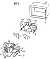
- FIGS 5 and 6 show a slightly modified embodiment.
- the relay 1 without the housing cap 11 is only equipped with its base plate 12.
- the housing cap 11 of the relay has an extension downward in the form of a collar 15.
- the base 40 is formed only by a base plate 41 without a circumferential peripheral wall, namely by overmoulding a lead frame 24, which in this example is designed with preformed conductor segments 25 and flat plugs 26 as in the previous example.
- This lead frame 24 is thus first encapsulated with plastic during assembly in order to obtain the rimless base 40.
- the board segments are separated by removing the intermediate webs 28 as in the previous one Example isolated from each other. This state is shown in FIG. 5.
- the base plate 41 is constructed in exactly the same way as the previously described base plate 21, for example also provided with chambers 30 for receiving the resistors 3.
- the relay 1 is placed on the base 40 without a cap, and, as before, the connecting pins 13 and the connecting wires 31 are soldered. This state is shown in FIG. 6.
- the housing cap 11 is now placed over this relay with a base according to FIG. 6, the collar 15 surrounding the base and in turn forming a cavity on its underside which is filled with potting compound.
- FIG. 7 Another embodiment is shown in FIG. 7.
- a relay 1 which is closed as in FIG. 1 with a housing cap and a base plate, is connected to an adapter which consists of a base plate (not shown) and a lead frame 44.
- the base plate is essentially designed in the same way as the base plate 41 in FIG. 5, the lead frame preferably being embedded.
- the individual conductor segments 45 are preferably separated after embedding, as is also described with reference to FIG. 5. It would also be conceivable to cut and embed the individual parts beforehand.
- the flat plugs 46 connected to the conductor segments 45 are not bent vertically from the bottom side downwards, but rather vertically from the bottom side upwards along the outer sides of the relay 1.
- the lead frame 44 is embedded in the material of the base plate, with as little protrusion as possible on the bottom side.
- resistors 3 or other components are positioned in chambers of the base plate, as in the previous exemplary embodiments, and relay 1 is attached.
- a frame-shaped sleeve 47 which is only indicated by dashed lines, is now over the tabs on the side of the housing cap 11 are pushed on, and only up to the bottom of the relay.
- the connecting pins 13 and the connecting wires 31 in the recesses of the conductor segments are easily accessible, so that the soldering can also be carried out by immersion in a solder bath.
- the sleeve 47 is then moved to a protrusion towards the underside of the adapter, so that the soldered joints lie in a cavity 48 surrounded by the edge of the sleeve.
- This cavity 48 is now filled with potting compound as in the previous exemplary embodiments.
Landscapes
- Physics & Mathematics (AREA)
- Electromagnetism (AREA)
- Connector Housings Or Holding Contact Members (AREA)
- Coupling Device And Connection With Printed Circuit (AREA)
- Manufacturing Of Electrical Connectors (AREA)
Applications Claiming Priority (2)
| Application Number | Priority Date | Filing Date | Title |
|---|---|---|---|
| DE4437954 | 1994-10-24 | ||
| DE4437954A DE4437954C1 (de) | 1994-10-24 | 1994-10-24 | Anordnung eines Relais mit einem Steckadapter und Verfahren zur Herstellung dieser Anordnung |
Publications (3)
| Publication Number | Publication Date |
|---|---|
| EP0713233A2 true EP0713233A2 (fr) | 1996-05-22 |
| EP0713233A3 EP0713233A3 (fr) | 1998-03-04 |
| EP0713233B1 EP0713233B1 (fr) | 1999-09-29 |
Family
ID=6531555
Family Applications (1)
| Application Number | Title | Priority Date | Filing Date |
|---|---|---|---|
| EP95116492A Expired - Lifetime EP0713233B1 (fr) | 1994-10-24 | 1995-10-19 | Agencement d'un relais avec un adaptateur à fiches et procédé pour la fabrication de cet agencement |
Country Status (4)
| Country | Link |
|---|---|
| US (1) | US5579211A (fr) |
| EP (1) | EP0713233B1 (fr) |
| JP (1) | JPH08255543A (fr) |
| DE (2) | DE4437954C1 (fr) |
Cited By (1)
| Publication number | Priority date | Publication date | Assignee | Title |
|---|---|---|---|---|
| FR3062948A1 (fr) * | 2017-02-16 | 2018-08-17 | Electricite De France | Ensemble constitue d'un relais et d'un adaptateur |
Families Citing this family (14)
| Publication number | Priority date | Publication date | Assignee | Title |
|---|---|---|---|---|
| DE19707709C1 (de) * | 1997-02-26 | 1998-04-16 | Siemens Ag | Leiterplatte für elektrische Schaltungen und Verfahren zur Herstellung einer solchen Leiterplatte, sowie Anordnung einer Leiterplatte auf einem Stecksockel |
| DE19813530A1 (de) * | 1998-03-26 | 1999-10-07 | Siemens Ag | Schallreduziertes Relais |
| DE19940347B4 (de) * | 1999-08-25 | 2006-06-08 | Siemens Ag | Elektrische Verbindungsvorrichtung zum Aufsetzen auf Anschlußstifte eines elektrischen Bausteins |
| DE19956498C2 (de) * | 1999-11-24 | 2002-08-14 | Tyco Electronics Logistics Ag | Anordnung eines Relais mit einem Adaptersockel |
| TWI243636B (en) * | 2004-06-10 | 2005-11-11 | Delta Electronics Inc | Assembling structure of electronic apparatus and assembling method therefor |
| DE102004032737B3 (de) * | 2004-07-07 | 2006-01-12 | Tyco Electronics Amp Gmbh | Relais, insbesondere für Steckmontage, und Verfahren zu dessen Herstellung |
| JP2007123314A (ja) * | 2005-10-25 | 2007-05-17 | Yazaki Corp | リレーモジュール及び電装ユニット |
| US7517235B2 (en) | 2006-12-28 | 2009-04-14 | General Electric Company | Press fit connection for mounting electrical plug-in outlet insulator to a busway aluminum housing |
| JP5997279B2 (ja) * | 2012-08-21 | 2016-09-28 | 矢崎総業株式会社 | 電子部品組立体と端子金具との接続構造、電子部品組立体を有する電気接続箱 |
| DE112014001302B4 (de) * | 2013-03-14 | 2024-02-08 | Yazaki Corporation | Montagestruktur einer Elektronikkomponente und eines elektrischen Verbindungskastens |
| US9159514B2 (en) * | 2013-11-18 | 2015-10-13 | Tyco Electronics Corporation | Relay connector assembly for a relay system |
| CN104112627A (zh) * | 2014-07-21 | 2014-10-22 | 赵士立 | 一种电柜箱电路接触器 |
| JP6413553B2 (ja) * | 2014-09-26 | 2018-10-31 | 富士電機株式会社 | パワー半導体モジュール装置 |
| CN106128858B (zh) * | 2016-08-24 | 2018-01-30 | 宁波汇洲电器有限公司 | 一种静音电磁继电器及其组装方法 |
Citations (2)
| Publication number | Priority date | Publication date | Assignee | Title |
|---|---|---|---|---|
| DE2810511A1 (de) | 1978-03-10 | 1979-09-13 | Siemens Ag | Adapter fuer ein elektrisches bauelement, insbesondere fuer ein relais, und verfahren zu dessen herstellung |
| US4400761A (en) | 1981-06-12 | 1983-08-23 | Trw Inc. | Compact relay system |
Family Cites Families (7)
| Publication number | Priority date | Publication date | Assignee | Title |
|---|---|---|---|---|
| US3714515A (en) * | 1971-09-20 | 1973-01-30 | Gen Electric | Housing assembly of modular construction for solid state relays with plural external terminals |
| US3809965A (en) * | 1973-03-26 | 1974-05-07 | Square D Co | Solid state relay and timer housing means |
| US3949276A (en) * | 1974-02-15 | 1976-04-06 | Elmeg Elektro-Mechanik Gmbh | Plug-in type relay |
| DE2618317C2 (de) * | 1976-04-27 | 1982-09-30 | Brown, Boveri & Cie Ag, 6800 Mannheim | Adapter zur Verbindung elektromagnetischer Schaltgeräte mit gedruckten Leiterplatten |
| JPS5797347U (fr) * | 1980-12-05 | 1982-06-15 | ||
| US4361371A (en) * | 1980-12-08 | 1982-11-30 | Amf Incorporated | Packaging of solid state relay |
| DE3425312A1 (de) * | 1984-07-10 | 1986-01-16 | Stribel GmbH, 7443 Frickenhausen | Elektromagnetisches relais |
-
1994
- 1994-10-24 DE DE4437954A patent/DE4437954C1/de not_active Expired - Lifetime
-
1995
- 1995-10-19 EP EP95116492A patent/EP0713233B1/fr not_active Expired - Lifetime
- 1995-10-19 DE DE59506944T patent/DE59506944D1/de not_active Expired - Fee Related
- 1995-10-23 JP JP7274020A patent/JPH08255543A/ja not_active Ceased
- 1995-10-23 US US08/546,673 patent/US5579211A/en not_active Expired - Fee Related
Patent Citations (2)
| Publication number | Priority date | Publication date | Assignee | Title |
|---|---|---|---|---|
| DE2810511A1 (de) | 1978-03-10 | 1979-09-13 | Siemens Ag | Adapter fuer ein elektrisches bauelement, insbesondere fuer ein relais, und verfahren zu dessen herstellung |
| US4400761A (en) | 1981-06-12 | 1983-08-23 | Trw Inc. | Compact relay system |
Cited By (2)
| Publication number | Priority date | Publication date | Assignee | Title |
|---|---|---|---|---|
| FR3062948A1 (fr) * | 2017-02-16 | 2018-08-17 | Electricite De France | Ensemble constitue d'un relais et d'un adaptateur |
| WO2018149955A1 (fr) * | 2017-02-16 | 2018-08-23 | Electricite De France | Ensemble constitué d'un relais et d'un adaptateur |
Also Published As
| Publication number | Publication date |
|---|---|
| DE59506944D1 (de) | 1999-11-04 |
| DE4437954C1 (de) | 1996-02-08 |
| EP0713233A3 (fr) | 1998-03-04 |
| JPH08255543A (ja) | 1996-10-01 |
| US5579211A (en) | 1996-11-26 |
| EP0713233B1 (fr) | 1999-09-29 |
Similar Documents
| Publication | Publication Date | Title |
|---|---|---|
| DE4323827C1 (de) | Steckbare Baugruppe | |
| DE69301202T2 (de) | Schwimmender elektrischer Steckverbinder | |
| DE69522015T2 (de) | Elektrischer Verbinder | |
| DE69909311T2 (de) | Zweiteiliger mikroelektronischer stecker und methode | |
| EP1080610B1 (fr) | Culot de lampe a decharge muni d'un dispositif d'amor age | |
| DE69024189T2 (de) | Doppelt isolierter Transformator des Koaxialtyps und sein Herstellungsverfahren | |
| EP0713233B1 (fr) | Agencement d'un relais avec un adaptateur à fiches et procédé pour la fabrication de cet agencement | |
| DE19605252B4 (de) | Oberflächenmontierbare elektrische Mikrominiatur-Schmelzsicherung | |
| DE2810514A1 (de) | Steckverbinder mit stoerschutz | |
| EP1199913B1 (fr) | Méthode de fabrication d'unités comprenant une feuille de circuit et un boítier de support | |
| DE10121654A1 (de) | Kästchenförmiger Kontakt mit Beanspruchungsbegrenzung | |
| DE19713008C1 (de) | Zentralelektrik für ein Kraftfahrzeug und Verfahren zu ihrer Herstellung | |
| DE69328662T2 (de) | Filterverbinder hoher Dichte | |
| WO2002051214A9 (fr) | Culot de lampe a decharge comportant un dispositif d'amorçage | |
| DE102018202669B3 (de) | Induktives Bauelement und Verfahren zur Herstellung eines induktiven Bauelements | |
| DE3343569C2 (de) | Miniatursicherung | |
| DE4310369C2 (de) | Kontaktsatz für einen Steckverbinder | |
| EP0495778B1 (fr) | Connecteur de filtrage | |
| DE4431274C2 (de) | Verfahren zum Herstellen eines Elektro-Installationsgerätes sowie Elektro-Installationsgerät | |
| DE2835963A1 (de) | Elektromagnetisches relais | |
| EP0758484A1 (fr) | Relais modulaire | |
| DE29720249U1 (de) | Elektromagnetisches Relais mit Schmelzsicherung | |
| EP0123872B1 (fr) | Barrière à diode Zéner | |
| DE19719436C2 (de) | Spritzgußgehäuse | |
| EP0692805A1 (fr) | Relais électrique |
Legal Events
| Date | Code | Title | Description |
|---|---|---|---|
| PUAI | Public reference made under article 153(3) epc to a published international application that has entered the european phase |
Free format text: ORIGINAL CODE: 0009012 |
|
| AK | Designated contracting states |
Kind code of ref document: A2 Designated state(s): DE FR GB IT |
|
| PUAL | Search report despatched |
Free format text: ORIGINAL CODE: 0009013 |
|
| AK | Designated contracting states |
Kind code of ref document: A3 Designated state(s): DE FR GB IT |
|
| 17P | Request for examination filed |
Effective date: 19980320 |
|
| GRAG | Despatch of communication of intention to grant |
Free format text: ORIGINAL CODE: EPIDOS AGRA |
|
| GRAG | Despatch of communication of intention to grant |
Free format text: ORIGINAL CODE: EPIDOS AGRA |
|
| GRAH | Despatch of communication of intention to grant a patent |
Free format text: ORIGINAL CODE: EPIDOS IGRA |
|
| 17Q | First examination report despatched |
Effective date: 19990316 |
|
| GRAH | Despatch of communication of intention to grant a patent |
Free format text: ORIGINAL CODE: EPIDOS IGRA |
|
| GRAA | (expected) grant |
Free format text: ORIGINAL CODE: 0009210 |
|
| AK | Designated contracting states |
Kind code of ref document: B1 Designated state(s): DE FR GB IT |
|
| REF | Corresponds to: |
Ref document number: 59506944 Country of ref document: DE Date of ref document: 19991104 |
|
| ET | Fr: translation filed | ||
| ITF | It: translation for a ep patent filed | ||
| GBT | Gb: translation of ep patent filed (gb section 77(6)(a)/1977) |
Effective date: 19991202 |
|
| PLBE | No opposition filed within time limit |
Free format text: ORIGINAL CODE: 0009261 |
|
| STAA | Information on the status of an ep patent application or granted ep patent |
Free format text: STATUS: NO OPPOSITION FILED WITHIN TIME LIMIT |
|
| 26N | No opposition filed | ||
| PGFP | Annual fee paid to national office [announced via postgrant information from national office to epo] |
Ref country code: DE Payment date: 20001030 Year of fee payment: 6 |
|
| REG | Reference to a national code |
Ref country code: GB Ref legal event code: 732E |
|
| REG | Reference to a national code |
Ref country code: GB Ref legal event code: IF02 |
|
| PG25 | Lapsed in a contracting state [announced via postgrant information from national office to epo] |
Ref country code: DE Free format text: LAPSE BECAUSE OF NON-PAYMENT OF DUE FEES Effective date: 20020702 |
|
| PGFP | Annual fee paid to national office [announced via postgrant information from national office to epo] |
Ref country code: GB Payment date: 20030915 Year of fee payment: 9 |
|
| PGFP | Annual fee paid to national office [announced via postgrant information from national office to epo] |
Ref country code: FR Payment date: 20031003 Year of fee payment: 9 |
|
| PG25 | Lapsed in a contracting state [announced via postgrant information from national office to epo] |
Ref country code: GB Free format text: LAPSE BECAUSE OF NON-PAYMENT OF DUE FEES Effective date: 20041019 |
|
| GBPC | Gb: european patent ceased through non-payment of renewal fee |
Effective date: 20041019 |
|
| PG25 | Lapsed in a contracting state [announced via postgrant information from national office to epo] |
Ref country code: FR Free format text: LAPSE BECAUSE OF NON-PAYMENT OF DUE FEES Effective date: 20050630 |
|
| REG | Reference to a national code |
Ref country code: FR Ref legal event code: ST |
|
| PG25 | Lapsed in a contracting state [announced via postgrant information from national office to epo] |
Ref country code: IT Free format text: LAPSE BECAUSE OF NON-PAYMENT OF DUE FEES;WARNING: LAPSES OF ITALIAN PATENTS WITH EFFECTIVE DATE BEFORE 2007 MAY HAVE OCCURRED AT ANY TIME BEFORE 2007. THE CORRECT EFFECTIVE DATE MAY BE DIFFERENT FROM THE ONE RECORDED. Effective date: 20051019 |