EP0692805A1 - Relais électrique - Google Patents
Relais électrique Download PDFInfo
- Publication number
- EP0692805A1 EP0692805A1 EP95110015A EP95110015A EP0692805A1 EP 0692805 A1 EP0692805 A1 EP 0692805A1 EP 95110015 A EP95110015 A EP 95110015A EP 95110015 A EP95110015 A EP 95110015A EP 0692805 A1 EP0692805 A1 EP 0692805A1
- Authority
- EP
- European Patent Office
- Prior art keywords
- housing
- relay
- press
- circuit board
- bottom side
- Prior art date
- Legal status (The legal status is an assumption and is not a legal conclusion. Google has not performed a legal analysis and makes no representation as to the accuracy of the status listed.)
- Granted
Links
Images
Classifications
-
- H—ELECTRICITY
- H05—ELECTRIC TECHNIQUES NOT OTHERWISE PROVIDED FOR
- H05K—PRINTED CIRCUITS; CASINGS OR CONSTRUCTIONAL DETAILS OF ELECTRIC APPARATUS; MANUFACTURE OF ASSEMBLAGES OF ELECTRICAL COMPONENTS
- H05K3/00—Apparatus or processes for manufacturing printed circuits
- H05K3/30—Assembling printed circuits with electric components, e.g. with resistors
- H05K3/32—Assembling printed circuits with electric components, e.g. with resistors electrically connecting electric components or wires to printed circuits
- H05K3/34—Assembling printed circuits with electric components, e.g. with resistors electrically connecting electric components or wires to printed circuits by soldering
- H05K3/341—Surface mounted components
- H05K3/3421—Leaded components
- H05K3/3426—Leaded components characterised by the leads
-
- H—ELECTRICITY
- H01—ELECTRIC ELEMENTS
- H01H—ELECTRIC SWITCHES; RELAYS; SELECTORS; EMERGENCY PROTECTIVE DEVICES
- H01H50/00—Details of electromagnetic relays
- H01H50/02—Bases; Casings; Covers
- H01H50/023—Details concerning sealing, e.g. sealing casing with resin
-
- H—ELECTRICITY
- H01—ELECTRIC ELEMENTS
- H01H—ELECTRIC SWITCHES; RELAYS; SELECTORS; EMERGENCY PROTECTIVE DEVICES
- H01H50/00—Details of electromagnetic relays
- H01H50/14—Terminal arrangements
-
- H—ELECTRICITY
- H05—ELECTRIC TECHNIQUES NOT OTHERWISE PROVIDED FOR
- H05K—PRINTED CIRCUITS; CASINGS OR CONSTRUCTIONAL DETAILS OF ELECTRIC APPARATUS; MANUFACTURE OF ASSEMBLAGES OF ELECTRICAL COMPONENTS
- H05K3/00—Apparatus or processes for manufacturing printed circuits
- H05K3/30—Assembling printed circuits with electric components, e.g. with resistors
- H05K3/306—Assembling printed circuits with electric components, e.g. with resistors with lead-in-hole components
- H05K3/308—Adaptations of leads
-
- H—ELECTRICITY
- H01—ELECTRIC ELEMENTS
- H01H—ELECTRIC SWITCHES; RELAYS; SELECTORS; EMERGENCY PROTECTIVE DEVICES
- H01H1/00—Contacts
- H01H1/58—Electric connections to or between contacts; Terminals
- H01H1/5805—Connections to printed circuits
-
- H—ELECTRICITY
- H01—ELECTRIC ELEMENTS
- H01H—ELECTRIC SWITCHES; RELAYS; SELECTORS; EMERGENCY PROTECTIVE DEVICES
- H01H1/00—Contacts
- H01H1/58—Electric connections to or between contacts; Terminals
- H01H2001/5888—Terminals of surface mounted devices [SMD]
-
- H—ELECTRICITY
- H05—ELECTRIC TECHNIQUES NOT OTHERWISE PROVIDED FOR
- H05K—PRINTED CIRCUITS; CASINGS OR CONSTRUCTIONAL DETAILS OF ELECTRIC APPARATUS; MANUFACTURE OF ASSEMBLAGES OF ELECTRICAL COMPONENTS
- H05K1/00—Printed circuits
- H05K1/02—Details
- H05K1/0271—Arrangements for reducing stress or warp in rigid printed circuit boards, e.g. caused by loads, vibrations or differences in thermal expansion
-
- H—ELECTRICITY
- H05—ELECTRIC TECHNIQUES NOT OTHERWISE PROVIDED FOR
- H05K—PRINTED CIRCUITS; CASINGS OR CONSTRUCTIONAL DETAILS OF ELECTRIC APPARATUS; MANUFACTURE OF ASSEMBLAGES OF ELECTRICAL COMPONENTS
- H05K1/00—Printed circuits
- H05K1/18—Printed circuits structurally associated with non-printed electric components
-
- H—ELECTRICITY
- H05—ELECTRIC TECHNIQUES NOT OTHERWISE PROVIDED FOR
- H05K—PRINTED CIRCUITS; CASINGS OR CONSTRUCTIONAL DETAILS OF ELECTRIC APPARATUS; MANUFACTURE OF ASSEMBLAGES OF ELECTRICAL COMPONENTS
- H05K2201/00—Indexing scheme relating to printed circuits covered by H05K1/00
- H05K2201/10—Details of components or other objects attached to or integrated in a printed circuit board
- H05K2201/10613—Details of electrical connections of non-printed components, e.g. special leads
- H05K2201/10742—Details of leads
- H05K2201/1075—Shape details
- H05K2201/10818—Flat leads
- H05K2201/10825—Distorted or twisted flat leads, i.e. deformed by torque
-
- H—ELECTRICITY
- H05—ELECTRIC TECHNIQUES NOT OTHERWISE PROVIDED FOR
- H05K—PRINTED CIRCUITS; CASINGS OR CONSTRUCTIONAL DETAILS OF ELECTRIC APPARATUS; MANUFACTURE OF ASSEMBLAGES OF ELECTRICAL COMPONENTS
- H05K2201/00—Indexing scheme relating to printed circuits covered by H05K1/00
- H05K2201/10—Details of components or other objects attached to or integrated in a printed circuit board
- H05K2201/10613—Details of electrical connections of non-printed components, e.g. special leads
- H05K2201/10742—Details of leads
- H05K2201/1075—Shape details
- H05K2201/10856—Divided leads, e.g. by slot in length direction of lead, or by branching of the lead
-
- H—ELECTRICITY
- H05—ELECTRIC TECHNIQUES NOT OTHERWISE PROVIDED FOR
- H05K—PRINTED CIRCUITS; CASINGS OR CONSTRUCTIONAL DETAILS OF ELECTRIC APPARATUS; MANUFACTURE OF ASSEMBLAGES OF ELECTRICAL COMPONENTS
- H05K3/00—Apparatus or processes for manufacturing printed circuits
- H05K3/30—Assembling printed circuits with electric components, e.g. with resistors
- H05K3/32—Assembling printed circuits with electric components, e.g. with resistors electrically connecting electric components or wires to printed circuits
- H05K3/34—Assembling printed circuits with electric components, e.g. with resistors electrically connecting electric components or wires to printed circuits by soldering
- H05K3/341—Surface mounted components
- H05K3/3421—Leaded components
-
- Y—GENERAL TAGGING OF NEW TECHNOLOGICAL DEVELOPMENTS; GENERAL TAGGING OF CROSS-SECTIONAL TECHNOLOGIES SPANNING OVER SEVERAL SECTIONS OF THE IPC; TECHNICAL SUBJECTS COVERED BY FORMER USPC CROSS-REFERENCE ART COLLECTIONS [XRACs] AND DIGESTS
- Y02—TECHNOLOGIES OR APPLICATIONS FOR MITIGATION OR ADAPTATION AGAINST CLIMATE CHANGE
- Y02P—CLIMATE CHANGE MITIGATION TECHNOLOGIES IN THE PRODUCTION OR PROCESSING OF GOODS
- Y02P70/00—Climate change mitigation technologies in the production process for final industrial or consumer products
- Y02P70/50—Manufacturing or production processes characterised by the final manufactured product
Definitions
- the invention relates to an electrical relay with a housing which has a bottom side for placement on a printed circuit board and emerge from the connecting conductor, which are provided with connecting lugs for contacting on the printed circuit board.
- connection conductors In conventional relays, the connection conductors usually emerge from the bottom of the housing, and the connection lugs they form are soldered into holes in the circuit board from the underside of the circuit board. Recently, more and more, especially for small components, the so-called surface mounting technology (SMT) has been used, the components resting with flat connecting lugs on the circuit board and being soldered by heat input from the top. This creates a unique, brief, but nevertheless high thermal load for the components.
- SMT surface mounting technology
- the connecting conductors emerging from the bottom side or from the side walls in the area near the bottom are bent parallel to the bottom side in these relays to form flat contacts (EP 0 171 808 B1).
- the aim of the present invention is to construct a relay of the type mentioned in the introduction in such a way that heat and mechanical press-in forces in the region of the connecting lugs cannot affect the sealing and the adjustment in the interior of the relay.
- this aim is achieved in that the connecting conductors emerge from the upper side of the housing facing away from the bottom side and extend with bent sections along side walls of the housing to the region of the bottom side where they form the connecting lugs.
- the main idea of the invention is therefore to turn the relay over compared to conventional designs, so that the connecting conductors do not emerge directly from the bottom or from the area near the floor, but from the top of the relay facing away from the printed circuit board and then downward by appropriate shaping on the housing sides are guided where they form the corresponding terminal lugs, are preferably designed as press-in handles.
- the connecting conductors have a large length, so that the forces which occur during the pressing in are not or only to a small extent Dimensions are transferred to the sealing zones located on the top of the housing, so there can be no damage to the tightness.
- voltages are decoupled from the press-in zones due to different thermal expansions of the relay and the printed circuit board. The press-in connection is therefore not at risk.
- connecting lugs When the connecting lugs are designed as press-in handles, the high temperature loads on the relay are completely eliminated, which under certain circumstances enables the use of inexpensive materials. Another advantage of the connecting conductors emerging at the top is that they are easily accessible for tests on the built-in relay.
- the invention is primarily designed for an application of the press-in technology, that is to say for the design of the connecting lugs as press-in stems, some of the advantages also come into play when the connecting lugs are designed for surface mounting (SMT).
- SMT surface mounting
- SMT soldering has a particularly favorable effect on the fact that the outlet side of the connecting conductor, which is formed by a base and by a sealing sealing compound which forms the bottom side in conventional relays, now forms the upper side in the relay designed according to the invention represents and faces the soldering heat radiation.
- the housing cap is usually made of a thermoplastic
- the base consists of a dimensionally stable material
- epoxy resin which is thermally used as a thermosetting material, is usually used as the sealing compound is much more stable.
- connection conductors of the relay running on the outside of the housing give rise to insulation problems with respect to neighboring components, these can be remedied by means of additional foils, but in particular by means of a subsequent cap made of insulating material.
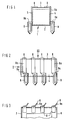
- the relay shown in Figures 1 to 3 has a housing 1, which contains an invisible, arbitrarily designed relay system in its interior.
- the housing has a closed bottom side 2 for placement on a printed circuit board, a top side 3 opposite the bottom side and longitudinal side walls 4 and 5 and transverse side walls 6 and 7. From the top 3, connecting conductors 8 emerge for the contacts and the coil winding of the relay, the bushings the connecting conductor and possibly other housing gaps are sealed in the top 3, as is usually done in the bottom side with conventional relays.
- the connecting conductors 8 formed from sheet metal strips are bent over the upper housing edges and run with their central sections 8a down along the longitudinal sides 4 and 5 of the relay, where they are bent off near the bottom side to form press-in handles 9 with press-in shoulders 9a formed on the upper side .
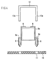
- a circuit board 10 has contact holes 11 which are laminated with conductive material in a known manner.
- a relay with the housing 1 and the press-in handles 9 is placed on the circuit board 10, so that the press-in handles 9 are aligned with the contact holes 11.
- a U-shaped press-in tool 12 With a U-shaped press-in tool 12, the legs 12a of which press on the press-in shoulders 9a, the press-in stems 9 are pressed into the bores 11 with the required press-in force and thus contacted.
- the side legs 12a of the press-in tool 12 are adapted to the outer contours of the housing 1 and the central sections 8a of the connecting conductors in such a way that the latter are held during the pressing in and are protected against bending.
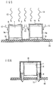
- FIG. 5 shows another embodiment of a relay according to the invention, specifically for surface mounting technology (SMT).
- SMT surface mounting technology
- the connection conductors 8 also emerge from the top of the housing 1, and as there the central sections 8a are led down along the side walls.
- the connection lugs are designed as SMT contacts 19, which are soldered to the surface of a hole-free printed circuit board 20.
- the soldering is carried out by introducing thermal radiation 13, which is quickly transported downward to the soldering points through the central sections 8a of the connecting conductors. In this way, the soldering time can be kept very short in order to keep the heat load on the housing as low as possible.
- the top of the housing with the exit points of the connecting conductors 8 can be covered by a reflective film 14. In any case, the advantages of a decoupling between the connecting lugs and the exit points of the connecting conductors from the housing also take effect in this SMT version of a relay.
- the connecting conductors each run over the flanks or on the outside of the housing side walls, the problem can arise under certain circumstances of ensuring adequate insulation with respect to an adjacent relay or another component.
- This can be done, for example, by inserting additional insulating foils between the components arranged on the printed circuit board.
- An advantageous embodiment is shown in Figure 6.
- an additional overcap 15 made of insulating material is used.
- This cap 15 is put over the actual relay housing 1 after assembly. It is dimensioned such that it also covers the connecting conductors 8 running on the outside of the housing and the press-in pins 9 or, if appropriate, also flat solder connections 19 according to FIG.
- Such an overcap can be produced in a simple manner by deep drawing or in some other way.
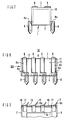
- FIGS. 7 to 9 A somewhat modified embodiment of a relay according to the invention is shown in FIGS. 7 to 9 in the same views as in FIGS. 1 to 3.
- the housing walls are reinforced, at least on the sides 4 and 5, so that raised sections 16 are formed, between which vertical grooves 17 receive the connecting conductor sections 8b.
- the housing can be stiffened, while the connecting conductors in the grooves 17 are set back somewhat in relation to the outer contour.
Landscapes
- Engineering & Computer Science (AREA)
- Physics & Mathematics (AREA)
- Electromagnetism (AREA)
- Manufacturing & Machinery (AREA)
- Microelectronics & Electronic Packaging (AREA)
- Coupling Device And Connection With Printed Circuit (AREA)
- Switch Cases, Indication, And Locking (AREA)
- Combinations Of Printed Boards (AREA)
- Structures For Mounting Electric Components On Printed Circuit Boards (AREA)
- Relay Circuits (AREA)
- Control Of Motors That Do Not Use Commutators (AREA)
Applications Claiming Priority (2)
| Application Number | Priority Date | Filing Date | Title |
|---|---|---|---|
| DE4425077 | 1994-07-15 | ||
| DE4425077 | 1994-07-15 |
Publications (2)
| Publication Number | Publication Date |
|---|---|
| EP0692805A1 true EP0692805A1 (fr) | 1996-01-17 |
| EP0692805B1 EP0692805B1 (fr) | 1998-06-03 |
Family
ID=6523280
Family Applications (1)
| Application Number | Title | Priority Date | Filing Date |
|---|---|---|---|
| EP95110015A Expired - Lifetime EP0692805B1 (fr) | 1994-07-15 | 1995-06-23 | Relais électrique |
Country Status (5)
| Country | Link |
|---|---|
| US (1) | US5606298A (fr) |
| EP (1) | EP0692805B1 (fr) |
| AT (1) | ATE167000T1 (fr) |
| DE (1) | DE59502391D1 (fr) |
| ES (1) | ES2117329T3 (fr) |
Cited By (1)
| Publication number | Priority date | Publication date | Assignee | Title |
|---|---|---|---|---|
| CN107275156A (zh) * | 2017-08-09 | 2017-10-20 | 贵州鑫阳科技股份有限公司 | 一种继电器 |
Families Citing this family (10)
| Publication number | Priority date | Publication date | Assignee | Title |
|---|---|---|---|---|
| JPH09213189A (ja) * | 1996-01-29 | 1997-08-15 | Niles Parts Co Ltd | 電磁継電器の構造 |
| CN101916690B (zh) * | 2010-08-19 | 2012-09-05 | 厦门宏发电声股份有限公司 | 一种拍合式电磁继电器 |
| JPWO2014030626A1 (ja) | 2012-08-21 | 2016-07-28 | 矢崎総業株式会社 | 電子部品、電子部品と端子金具との接続構造、電子部品を有する電気接続箱 |
| JP6031322B2 (ja) * | 2012-10-15 | 2016-11-24 | 矢崎総業株式会社 | リレーモジュール及び電気接続箱 |
| WO2014142246A1 (fr) | 2013-03-14 | 2014-09-18 | 矢崎総業株式会社 | Structure d'assemblage de composant électronique et boîtier de jonction |
| US10123429B2 (en) * | 2016-07-20 | 2018-11-06 | Infineon Technologies Austria Ag | Mounting of components on a printed circuit board |
| CN107946141B (zh) * | 2017-11-29 | 2020-03-27 | 厦门宏发汽车电子有限公司 | 一种带u型弹片的引出脚及其静音继电器 |
| US10685800B2 (en) * | 2018-06-18 | 2020-06-16 | Edward W. Anderson | Testable sealed relay and self-diagnosing relay |
| WO2020157563A2 (fr) * | 2019-01-29 | 2020-08-06 | Appleton Grp, Llc | Gaine d'absorption de chaleur et de dissipation de chaleur pour un terminal d'un dispositif électrique |
| WO2024114759A1 (fr) * | 2022-12-01 | 2024-06-06 | 厦门宏发电力电器有限公司 | Relais |
Citations (6)
| Publication number | Priority date | Publication date | Assignee | Title |
|---|---|---|---|---|
| GB2050906A (en) * | 1979-06-13 | 1981-01-14 | Cii Honeywell Bull | Non-destructive dismantling of a modular electronic component |
| DE3430589A1 (de) * | 1984-08-20 | 1986-02-27 | Siemens AG, 1000 Berlin und 8000 München | Sockel fuer ein elektromagnetisches relais |
| EP0171808B1 (fr) | 1984-08-17 | 1989-05-03 | Siemens Aktiengesellschaft | Socle d'un relais électromagnétique |
| JPH03127424A (ja) * | 1989-10-12 | 1991-05-30 | Fujitsu Ltd | 電磁継電器 |
| JPH05217479A (ja) * | 1992-02-05 | 1993-08-27 | Fujitsu Ltd | 表面実装型電磁継電器 |
| JPH06150798A (ja) * | 1992-11-10 | 1994-05-31 | Nec Corp | 表面実装型電磁継電器 |
Family Cites Families (2)
| Publication number | Priority date | Publication date | Assignee | Title |
|---|---|---|---|---|
| ATE121560T1 (de) * | 1989-07-20 | 1995-05-15 | Omron Tateisi Electronics Co | Anschlusskontaktform für elektromagnetisches relais. |
| US5007844A (en) * | 1990-01-17 | 1991-04-16 | Hewlett-Packard Company | Surface mount method and device |
-
1995
- 1995-06-23 ES ES95110015T patent/ES2117329T3/es not_active Expired - Lifetime
- 1995-06-23 DE DE59502391T patent/DE59502391D1/de not_active Expired - Fee Related
- 1995-06-23 AT AT95110015T patent/ATE167000T1/de not_active IP Right Cessation
- 1995-06-23 EP EP95110015A patent/EP0692805B1/fr not_active Expired - Lifetime
- 1995-06-29 US US08/496,516 patent/US5606298A/en not_active Expired - Fee Related
Patent Citations (7)
| Publication number | Priority date | Publication date | Assignee | Title |
|---|---|---|---|---|
| GB2050906A (en) * | 1979-06-13 | 1981-01-14 | Cii Honeywell Bull | Non-destructive dismantling of a modular electronic component |
| EP0171808B1 (fr) | 1984-08-17 | 1989-05-03 | Siemens Aktiengesellschaft | Socle d'un relais électromagnétique |
| DE3430589A1 (de) * | 1984-08-20 | 1986-02-27 | Siemens AG, 1000 Berlin und 8000 München | Sockel fuer ein elektromagnetisches relais |
| DE3430589C2 (fr) | 1984-08-20 | 1991-02-28 | Siemens Ag, 1000 Berlin Und 8000 Muenchen, De | |
| JPH03127424A (ja) * | 1989-10-12 | 1991-05-30 | Fujitsu Ltd | 電磁継電器 |
| JPH05217479A (ja) * | 1992-02-05 | 1993-08-27 | Fujitsu Ltd | 表面実装型電磁継電器 |
| JPH06150798A (ja) * | 1992-11-10 | 1994-05-31 | Nec Corp | 表面実装型電磁継電器 |
Non-Patent Citations (3)
| Title |
|---|
| PATENT ABSTRACTS OF JAPAN vol. 015, no. 334 (E - 1104) 26 August 1991 (1991-08-26) * |
| PATENT ABSTRACTS OF JAPAN vol. 017, no. 653 (E - 1469) 3 December 1993 (1993-12-03) * |
| PATENT ABSTRACTS OF JAPAN vol. 018, no. 455 (E - 1595) 24 August 1994 (1994-08-24) * |
Cited By (1)
| Publication number | Priority date | Publication date | Assignee | Title |
|---|---|---|---|---|
| CN107275156A (zh) * | 2017-08-09 | 2017-10-20 | 贵州鑫阳科技股份有限公司 | 一种继电器 |
Also Published As
| Publication number | Publication date |
|---|---|
| US5606298A (en) | 1997-02-25 |
| ATE167000T1 (de) | 1998-06-15 |
| DE59502391D1 (de) | 1998-07-09 |
| ES2117329T3 (es) | 1998-08-01 |
| EP0692805B1 (fr) | 1998-06-03 |
Similar Documents
| Publication | Publication Date | Title |
|---|---|---|
| EP1430491B1 (fr) | Transformateur plat a bobines secondaires enfichees | |
| DE3318135C2 (fr) | ||
| DE4323827C1 (de) | Steckbare Baugruppe | |
| DE69635518T2 (de) | Kunststoffpackung für elektronische Anordnungen | |
| DE69524702T2 (de) | Elektrischer Verbindungskasten | |
| DE69817220T2 (de) | Oberflächenmontierter federkontaktstreifen und emi gehause | |
| DE19605252B4 (de) | Oberflächenmontierbare elektrische Mikrominiatur-Schmelzsicherung | |
| EP0692805B1 (fr) | Relais électrique | |
| DE69521249T2 (de) | Verdrahtungskonstruktion einer elektrischen Anschlussdose | |
| EP1714533B1 (fr) | Composant electrique comprenant une fiche de contact electroconductrice et destine a etre enfonce dans un orifice d'une carte de circuits imprimes | |
| EP0713233A2 (fr) | Agencement d'un relais avec un adaptateur à fiches et procédé pour la fabrication de cet agencement | |
| DE10053389A1 (de) | Verbindungsstruktur für elektrische Komponenten einer Leiterplatte | |
| DE102004041173A1 (de) | Lötaufbau zwischen einem Streifen einer Stromschiene und einem bedruckten Substrat | |
| DE102012218433B4 (de) | Kontaktanordnung | |
| EP0765110A1 (fr) | Plaquette de circuit et son procédé de fabrication | |
| AT390695B (de) | T-foermiger elektrischer verbinder | |
| DE4406200C1 (de) | Stiftförmiges Kontaktelement | |
| DE60014480T2 (de) | Elektronikgehäuse | |
| DE3444667A1 (de) | Kontaktbruecke fuer in gleicher ebene angeordnete leiterplatten in elektrischen und elektronischen geraeten und anlagen | |
| DE4203239A1 (de) | Schalterstecker | |
| EP3740050B1 (fr) | Carte de circuit imprimé dotée d'un connecteur enfichable | |
| DE19833248C2 (de) | Vorrichtung zum Führen und Massekontaktieren von Leiterplatten | |
| DE102022213610A1 (de) | Kontaktierung einer flexiblen Leiterfolie mit einer starren Leiterplatte sowie Verfahren zur Herstellung einer derartigen Kontaktierung | |
| DE3629296A1 (de) | Baugruppe der nachrichtentechnik | |
| EP0537314B1 (fr) | Mandrin de bobine et procede pour sa fabrication |
Legal Events
| Date | Code | Title | Description |
|---|---|---|---|
| PUAI | Public reference made under article 153(3) epc to a published international application that has entered the european phase |
Free format text: ORIGINAL CODE: 0009012 |
|
| AK | Designated contracting states |
Kind code of ref document: A1 Designated state(s): AT CH DE ES FR GB IT LI |
|
| 17P | Request for examination filed |
Effective date: 19960205 |
|
| 17Q | First examination report despatched |
Effective date: 19970401 |
|
| GRAG | Despatch of communication of intention to grant |
Free format text: ORIGINAL CODE: EPIDOS AGRA |
|
| GRAG | Despatch of communication of intention to grant |
Free format text: ORIGINAL CODE: EPIDOS AGRA |
|
| GRAH | Despatch of communication of intention to grant a patent |
Free format text: ORIGINAL CODE: EPIDOS IGRA |
|
| GRAH | Despatch of communication of intention to grant a patent |
Free format text: ORIGINAL CODE: EPIDOS IGRA |
|
| GRAA | (expected) grant |
Free format text: ORIGINAL CODE: 0009210 |
|
| AK | Designated contracting states |
Kind code of ref document: B1 Designated state(s): AT CH DE ES FR GB IT LI |
|
| REF | Corresponds to: |
Ref document number: 167000 Country of ref document: AT Date of ref document: 19980615 Kind code of ref document: T |
|
| PGFP | Annual fee paid to national office [announced via postgrant information from national office to epo] |
Ref country code: AT Payment date: 19980604 Year of fee payment: 4 |
|
| REG | Reference to a national code |
Ref country code: CH Ref legal event code: NV Representative=s name: SIEMENS SCHWEIZ AG Ref country code: CH Ref legal event code: EP |
|
| PGFP | Annual fee paid to national office [announced via postgrant information from national office to epo] |
Ref country code: FR Payment date: 19980624 Year of fee payment: 4 |
|
| PGFP | Annual fee paid to national office [announced via postgrant information from national office to epo] |
Ref country code: ES Payment date: 19980630 Year of fee payment: 4 |
|
| REF | Corresponds to: |
Ref document number: 59502391 Country of ref document: DE Date of ref document: 19980709 |
|
| REG | Reference to a national code |
Ref country code: ES Ref legal event code: FG2A Ref document number: 2117329 Country of ref document: ES Kind code of ref document: T3 |
|
| ET | Fr: translation filed | ||
| PGFP | Annual fee paid to national office [announced via postgrant information from national office to epo] |
Ref country code: DE Payment date: 19980819 Year of fee payment: 4 |
|
| ITF | It: translation for a ep patent filed | ||
| GBT | Gb: translation of ep patent filed (gb section 77(6)(a)/1977) |
Effective date: 19980807 |
|
| PLBE | No opposition filed within time limit |
Free format text: ORIGINAL CODE: 0009261 |
|
| STAA | Information on the status of an ep patent application or granted ep patent |
Free format text: STATUS: NO OPPOSITION FILED WITHIN TIME LIMIT |
|
| 26N | No opposition filed | ||
| PG25 | Lapsed in a contracting state [announced via postgrant information from national office to epo] |
Ref country code: GB Free format text: LAPSE BECAUSE OF NON-PAYMENT OF DUE FEES Effective date: 19990623 Ref country code: AT Free format text: LAPSE BECAUSE OF NON-PAYMENT OF DUE FEES Effective date: 19990623 |
|
| PG25 | Lapsed in a contracting state [announced via postgrant information from national office to epo] |
Ref country code: ES Free format text: LAPSE BECAUSE OF NON-PAYMENT OF DUE FEES Effective date: 19990624 |
|
| PG25 | Lapsed in a contracting state [announced via postgrant information from national office to epo] |
Ref country code: LI Free format text: LAPSE BECAUSE OF NON-PAYMENT OF DUE FEES Effective date: 19990630 Ref country code: FR Free format text: THE PATENT HAS BEEN ANNULLED BY A DECISION OF A NATIONAL AUTHORITY Effective date: 19990630 Ref country code: CH Free format text: LAPSE BECAUSE OF NON-PAYMENT OF DUE FEES Effective date: 19990630 |
|
| GBPC | Gb: european patent ceased through non-payment of renewal fee |
Effective date: 19990623 |
|
| REG | Reference to a national code |
Ref country code: CH Ref legal event code: PL |
|
| PG25 | Lapsed in a contracting state [announced via postgrant information from national office to epo] |
Ref country code: DE Free format text: LAPSE BECAUSE OF NON-PAYMENT OF DUE FEES Effective date: 20000503 |
|
| REG | Reference to a national code |
Ref country code: FR Ref legal event code: ST |
|
| REG | Reference to a national code |
Ref country code: ES Ref legal event code: FD2A Effective date: 20010403 |
|
| PG25 | Lapsed in a contracting state [announced via postgrant information from national office to epo] |
Ref country code: IT Free format text: LAPSE BECAUSE OF NON-PAYMENT OF DUE FEES Effective date: 20050623 |