EP0714136A1 - Elément semi-conducteur à hétérojunction ou avec barrière Schottky et cellule solaire - Google Patents
Elément semi-conducteur à hétérojunction ou avec barrière Schottky et cellule solaire Download PDFInfo
- Publication number
- EP0714136A1 EP0714136A1 EP95117698A EP95117698A EP0714136A1 EP 0714136 A1 EP0714136 A1 EP 0714136A1 EP 95117698 A EP95117698 A EP 95117698A EP 95117698 A EP95117698 A EP 95117698A EP 0714136 A1 EP0714136 A1 EP 0714136A1
- Authority
- EP
- European Patent Office
- Prior art keywords
- type
- thin film
- semiconductor element
- schottky
- type semiconductor
- Prior art date
- Legal status (The legal status is an assumption and is not a legal conclusion. Google has not performed a legal analysis and makes no representation as to the accuracy of the status listed.)
- Withdrawn
Links
Images


Classifications
-
- H—ELECTRICITY
- H10—SEMICONDUCTOR DEVICES; ELECTRIC SOLID-STATE DEVICES NOT OTHERWISE PROVIDED FOR
- H10K—ORGANIC ELECTRIC SOLID-STATE DEVICES
- H10K30/00—Organic devices sensitive to infrared radiation, light, electromagnetic radiation of shorter wavelength or corpuscular radiation
- H10K30/10—Organic devices sensitive to infrared radiation, light, electromagnetic radiation of shorter wavelength or corpuscular radiation comprising heterojunctions between organic semiconductors and inorganic semiconductors
-
- B—PERFORMING OPERATIONS; TRANSPORTING
- B82—NANOTECHNOLOGY
- B82Y—SPECIFIC USES OR APPLICATIONS OF NANOSTRUCTURES; MEASUREMENT OR ANALYSIS OF NANOSTRUCTURES; MANUFACTURE OR TREATMENT OF NANOSTRUCTURES
- B82Y10/00—Nanotechnology for information processing, storage or transmission, e.g. quantum computing or single electron logic
-
- H—ELECTRICITY
- H10—SEMICONDUCTOR DEVICES; ELECTRIC SOLID-STATE DEVICES NOT OTHERWISE PROVIDED FOR
- H10D—INORGANIC ELECTRIC SEMICONDUCTOR DEVICES
- H10D62/00—Semiconductor bodies, or regions thereof, of devices having potential barriers
- H10D62/80—Semiconductor bodies, or regions thereof, of devices having potential barriers characterised by the materials
- H10D62/82—Heterojunctions
- H10D62/822—Heterojunctions comprising only Group IV materials heterojunctions, e.g. Si/Ge heterojunctions
-
- H—ELECTRICITY
- H10—SEMICONDUCTOR DEVICES; ELECTRIC SOLID-STATE DEVICES NOT OTHERWISE PROVIDED FOR
- H10K—ORGANIC ELECTRIC SOLID-STATE DEVICES
- H10K85/00—Organic materials used in the body or electrodes of devices covered by this subclass
- H10K85/20—Carbon compounds, e.g. carbon nanotubes or fullerenes
-
- H—ELECTRICITY
- H10—SEMICONDUCTOR DEVICES; ELECTRIC SOLID-STATE DEVICES NOT OTHERWISE PROVIDED FOR
- H10K—ORGANIC ELECTRIC SOLID-STATE DEVICES
- H10K85/00—Organic materials used in the body or electrodes of devices covered by this subclass
- H10K85/60—Organic compounds having low molecular weight
- H10K85/615—Polycyclic condensed aromatic hydrocarbons, e.g. anthracene
-
- H—ELECTRICITY
- H10—SEMICONDUCTOR DEVICES; ELECTRIC SOLID-STATE DEVICES NOT OTHERWISE PROVIDED FOR
- H10K—ORGANIC ELECTRIC SOLID-STATE DEVICES
- H10K85/00—Organic materials used in the body or electrodes of devices covered by this subclass
- H10K85/60—Organic compounds having low molecular weight
- H10K85/615—Polycyclic condensed aromatic hydrocarbons, e.g. anthracene
- H10K85/624—Polycyclic condensed aromatic hydrocarbons, e.g. anthracene containing six or more rings
-
- H—ELECTRICITY
- H10—SEMICONDUCTOR DEVICES; ELECTRIC SOLID-STATE DEVICES NOT OTHERWISE PROVIDED FOR
- H10K—ORGANIC ELECTRIC SOLID-STATE DEVICES
- H10K30/00—Organic devices sensitive to infrared radiation, light, electromagnetic radiation of shorter wavelength or corpuscular radiation
- H10K30/50—Photovoltaic [PV] devices
-
- H—ELECTRICITY
- H10—SEMICONDUCTOR DEVICES; ELECTRIC SOLID-STATE DEVICES NOT OTHERWISE PROVIDED FOR
- H10K—ORGANIC ELECTRIC SOLID-STATE DEVICES
- H10K71/00—Manufacture or treatment specially adapted for the organic devices covered by this subclass
- H10K71/10—Deposition of organic active material
- H10K71/16—Deposition of organic active material using physical vapour deposition [PVD], e.g. vacuum deposition or sputtering
-
- Y—GENERAL TAGGING OF NEW TECHNOLOGICAL DEVELOPMENTS; GENERAL TAGGING OF CROSS-SECTIONAL TECHNOLOGIES SPANNING OVER SEVERAL SECTIONS OF THE IPC; TECHNICAL SUBJECTS COVERED BY FORMER USPC CROSS-REFERENCE ART COLLECTIONS [XRACs] AND DIGESTS
- Y02—TECHNOLOGIES OR APPLICATIONS FOR MITIGATION OR ADAPTATION AGAINST CLIMATE CHANGE
- Y02E—REDUCTION OF GREENHOUSE GAS [GHG] EMISSIONS, RELATED TO ENERGY GENERATION, TRANSMISSION OR DISTRIBUTION
- Y02E10/00—Energy generation through renewable energy sources
- Y02E10/50—Photovoltaic [PV] energy
- Y02E10/549—Organic PV cells
Definitions
- the present invention relates to a heterojunction type or Schottky-barrier type semiconductor element and a solar cell. More particularly, the present invention relates to a novel heterojunction type or Schottky-barrier type semiconductor element comprising a carbonaceous thin film, which is applicable as an electronic device, a solar cell and so on.
- Carbonaceous materials typically represented by graphite having excellent chemical, mechanical, biological and electronic properties are known to be applicable in a wide range of areas including space technology, sporting goods, and biological materials. Furthermore, the important role which may be played by carbonaceous ⁇ electronic materials as next-generation electronic materials is now entertained, in view of such electronic properties as ultra-high speed electron mobility and ultra-polarizability of graphite.
- carbonaceous materials come under the category of semiconductor materials.
- the carbonaceous materials heat-treated at a temperature of up to 800°C shows a positive Hall constant. According as the heat-treatment temperature becomes higher, the Hall constant decreases and changes into a negative one at a temperature of over 800°C.
- the sign of Hall constant once changes into positive at about 1,600°C along with a further increase in temperature, and changes again into negative at 2,400°C. This property of the carbonaceous materials suggests the possibility of making an electronic device by utilizing this property.
- the solar cells practically used at present mainly comprise silicon semiconductor and compound semiconductor, but not one made of organic materials.
- active research efforts have been made on solar cells utilizing organic thin films since invention of conductive polyacetylene in 1977.
- a major problem involved in current organic solar cells is that they are poor in stability and low in energy cenversion ratio.
- the present invention has an object to provide means to permit achievement of a semiconductor element by a new approach to carbonaceous materials. More specifically, the present invention has an object to achieve an optoelectric conversion diode and a solar cell using an amorphous carbonaceous thin film as an application of carbonaceous materials to electronic devices.
- the present invention provides a heterojunction type or Schottky-barier type semiconductor element wherein a carbonaceous thin film is chemically vapor-deposited (CVD) on an n-type or p-type semiconductor substrate and a solar cell as an application thereof.
- CVD chemically vapor-deposited
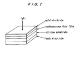
- Figure 1 shows a perspective view illustrating the construction of a carbonaceous thin film/n-type silicon multilayer sample of the present invention.
- Figure 2 shows an I-V characteristic diagram of a carbonaceous thin film/n-type silicon multilayer sample as an embodiment.
- Figure 3 shows a semi-logarithmic I-V characteristic diagram of a carbonaceous thin film/n-type silicon multilayer sample as an embodiment.
- Figure 4 shows a spectroscopic characteristic diagram of a carbonaceous thin film/n-type silicon multilayer sample as an embodiment.
- Figure 5 shows a relational diagram illustrating an absorption spectrum of a carbonaceous thin film as an embodiment.
- Figure 6 shows a schematic view illustrating the junction band structure of a 500°C carbonaceous thin film/n-type silicon multilayer sample as an embodiment.
- Figure 7 shows a temperature characteristic diagram illustrating for the optical band gap Eopt of a carbonaceous thin film as an embodiment.
- the present invention permits achievement of a novel semiconductor element not known so far by the use of the chemically vapor-deposited carbonaceous thin film and the n-type or p-type semiconductor substrate as described above, and allows application thereof to, for example, a diode, a rectifier element, a photodiode, an optical sensor and a solar cell.
- any n-type or p-type semiconductor substrate may be used: monocrystalline silicon, polycrystalline silicon, amorphous silicon, or compound semiconductor, or other n-type or p-type semiconductor substrate corresponding to any one thereof, in the form of a sheet or a thin film.
- the carbonaceous thin film to be chemically vapor-deposited (CVD) on such a semiconductor substrate may be formed from at least a kind of organic compound, particularly a carbocyclic organic compound as the raw material in the present invention.
- This carbocyclic organic compound may be selected from a wide range of kinds of compounds including hexacyclic benzene compounds and pentacyclic or septocyclic no-benzene compounds. Even a monocyclic or polycyclic organic compound including a pentacyclic or septocyclic one may be preferably employed in the present invention.
- any compound selected from a quinone hexacyclic compound such as 2,5-dimethyl-p-benzoquinone of the following formula:
- an organic compound containing such atoms as oxygen, nitrogen, boron, phosphorus and halogen as hetero-elements may be used as a kind of carbocyclic compound.
- a carbonaceous thin film of the present invention can be formed on said n-type or p-type semiconductor substrate by thermochemical vapor deposition.
- a material different from the carbon source material may be used as the source materials of the above-mentioned hetero-atom in the form of doping.
- the chemically vapor-deposited carbonaceous thin film should preferably comprise at least 80% (weight percentage) carbon. With a carbon content of under 80%, it is difficult to obtain a desired element having marked or stable properties as desired.
- the carbonaceous thin film should mainly comprise a non-diamond structure.
- the structure commonly known as the diamond structure, exhibiting insulating property, is naturally named as such.
- the non-diamond structure is considered to be formed by a structure in which a conjugate system of the carbonaceous compound in the above-mentioned carbonaceous thin film sufficiently expands.
- a preferable embodiment comprises, a carbocyclic organic compound as the raw material and a temperature up to 1000°C.
- the heterojunction type or Schottky-barrier type semiconductor element provided by the present invention has specific photoelectric characteristics and is expected to be applied to a solar cell or the like.
- n-type silicon monocrystalline wafer with phosphorus (P) as dopant having a thickness of 0.5 mm, was used as the substrate.
- the substrate Prior to depositing a carbonaceous thin film, the substrate was washed with fluoric acid in a concentration of 20%.
- the raw material for CVD reaction was 2,5-dimethyl-p-benzoquinone.
- the CVD reaction was caused under the following conditions under the atmospheric pressure: Substrate temperature: 500°C Material vaporizing temperature: 110°C Carrier gas: argon Depositing time: 90 minutes
- the thus deposited carbonaceous thin film had a thickness of about 400 ⁇ .
- alloy electrodes were attached to the back of the silicon substrate by ultrasonic welding.
- a gold thin film having a thickness of 80 to 100 ⁇ was vacuum-deposited on the surface of the carbonaceous thin film to form a surface electrode.
- the structure of the thus prepared cell sample is illustrated in Fig. 1.
- Fig. 2 shows current-voltage (I-V) characteristics of the prepared carbonaceous thin film/n-type silicon multilayer cell sample. Without light irradiation, this sample exhibits rectifying I-V characteristics.
- I-V current-voltage
- the sample When irradiating a light (Xe arc lamp) having a wavelength 400 to 850 nm and a power of 15 mW/cm2 onto it, the sample generated short-circuit current I sc of about 2.73 mA/cm2 and open-circuit voltage V oc of 325 mV.
- the fill factor value ff as derived from the I-V curve is about 0.65 and the energy conversion efficiency ⁇ is about 3.8%.
- Fig. 3 shows I-V characteristics of the sample without light irradiation, as measured at room temperature, in the form of a semi-logarithmic graph.
- the current-voltage relationship of the linear portion gives an ideality factor n and a dark current I o , as determined by the following formula, of 1.10 and 1.5 x 10 ⁇ 5 mA/cm2, respectively:
- Fig. 4 illustrates dependence on light wavelength (also known as spectroscopic characteristic) of short-circuit current and open-circuit voltage of this sample.
- This sample generates an almost constant photocurrent within a wavelength range of from 500 to 950 nm. This suggests the possibility of highly efficiently utilizing solar energy by the carbonaceous thin film/n-type silicon multilayer cell, and permits confirmation that this cell constitutes a solar cell or the like as an element known as a photoelectric transducer.
- the substrate Prior to depositing a carbonaceous thin film, the substrate was washed with fluoric acid in a concentration of 20%.
- the raw material for CVD reaction was ⁇ , ⁇ '-dichloro-p-xylene.
- the CVD reaction was caused under the atmospheric pressure under the following conditions: Substrate temperature: 800°C Material vaporizing temperature: 100°C Carrier gas: argon Depositing time: 120 minutes
- the resultant carbonaceous thin film had a thickness of about 500 ⁇ .
- alloy electrodes were attached to the back of the substrate by ultrasonic welding.
- gold was vacuum-deposited into a thickness of 80 to 100 ⁇ on the surface of the carbonaceous thin film as a sufrace electrode.
- this sample When light was not irradiated, this sample showed rectifying I-V characteristics.
- irradiating light Xe arc lamp
- the sample When irradiating light (Xe arc lamp) of a wavelength of 400 to 850 nm and a power of 40 mW/cm2, the sample generated short-circuit current I sc of about 0.26 mA/cm2 and open-circuit voltage V oc of 68 mV.
- the optical band gap E opt of the 500°C carbonaceous thin film as determined by this Formula (2) is about 0.25 eV.
- the 500°C carbonaceous thin film has a band gap of 0.25 eV, as described above.
- the junction type of the carbonaceous thin film/silicon multilayer sample is considered to be heterojunction.
- a typical junction band structure of the 500°C carbonaceous thin film/n-type silicon multilayer sample is shown in Fig. 6.
- Fig. 7 shows the optical band gap Eopt of carbonaceous thin film.
- the carbonaceous thin film heat-treated at a temperature of up to 580°C shows a positive optical band gap Eopt, the optical band gap Eopt changes into a negative one at a temparature of over 580°C.
- junction type of the carbonaceous thin film/semiconductor multilayer sample made at a temperature of up to 580°C is considered to be heterojunction type, and one made at a temperature of over 580°C is considered to be Schottky-barrier type.
- a heterojunction type or Schottky-barrier type semiconductor element comprising a chemical vapor-deposited (CVD) carbonaceous thin film and an n-type or p-type semiconductor substrate was successfully prepared.
- CVD chemical vapor-deposited
Landscapes
- Engineering & Computer Science (AREA)
- Chemical & Material Sciences (AREA)
- Physics & Mathematics (AREA)
- Nanotechnology (AREA)
- Materials Engineering (AREA)
- Mathematical Physics (AREA)
- Theoretical Computer Science (AREA)
- Crystallography & Structural Chemistry (AREA)
- Inorganic Chemistry (AREA)
- Electromagnetism (AREA)
- Spectroscopy & Molecular Physics (AREA)
- Photovoltaic Devices (AREA)
Applications Claiming Priority (4)
| Application Number | Priority Date | Filing Date | Title |
|---|---|---|---|
| JP274781/94 | 1994-11-09 | ||
| JP27478194 | 1994-11-09 | ||
| JP280596/95 | 1995-10-27 | ||
| JP28059695 | 1995-10-27 |
Publications (1)
| Publication Number | Publication Date |
|---|---|
| EP0714136A1 true EP0714136A1 (fr) | 1996-05-29 |
Family
ID=26551195
Family Applications (1)
| Application Number | Title | Priority Date | Filing Date |
|---|---|---|---|
| EP95117698A Withdrawn EP0714136A1 (fr) | 1994-11-09 | 1995-11-09 | Elément semi-conducteur à hétérojunction ou avec barrière Schottky et cellule solaire |
Country Status (1)
| Country | Link |
|---|---|
| EP (1) | EP0714136A1 (fr) |
Cited By (6)
| Publication number | Priority date | Publication date | Assignee | Title |
|---|---|---|---|---|
| KR100421650B1 (ko) * | 1998-06-15 | 2004-03-10 | 키시모토 상교 컴퍼니 리미티드 | 반도체 장치용 절연막 및 반도체 장치 |
| WO2005081296A1 (fr) * | 2004-02-10 | 2005-09-01 | Infineon Technologies Ag | Procede servant a deposer un materiau de carbone conducteur sur un semi-conducteur pour creer un contact schottky et dispositif de contact de semi-conducteur |
| US7768016B2 (en) | 2008-02-11 | 2010-08-03 | Qimonda Ag | Carbon diode array for resistivity changing memories |
| US7894253B2 (en) | 2006-10-27 | 2011-02-22 | Qimonda Ag | Carbon filament memory and fabrication method |
| US7915603B2 (en) | 2006-10-27 | 2011-03-29 | Qimonda Ag | Modifiable gate stack memory element |
| US8030637B2 (en) | 2006-08-25 | 2011-10-04 | Qimonda Ag | Memory element using reversible switching between SP2 and SP3 hybridized carbon |
Citations (1)
| Publication number | Priority date | Publication date | Assignee | Title |
|---|---|---|---|---|
| EP0472054A1 (fr) * | 1990-08-20 | 1992-02-26 | Siemens Aktiengesellschaft | Cellule photoélectrique comprenant du carbone hydrogéné amorphe |
-
1995
- 1995-11-09 EP EP95117698A patent/EP0714136A1/fr not_active Withdrawn
Patent Citations (1)
| Publication number | Priority date | Publication date | Assignee | Title |
|---|---|---|---|---|
| EP0472054A1 (fr) * | 1990-08-20 | 1992-02-26 | Siemens Aktiengesellschaft | Cellule photoélectrique comprenant du carbone hydrogéné amorphe |
Non-Patent Citations (5)
| Title |
|---|
| BHAGAVAT G K ET AL: "Semiconducting amorphous carbon films and carbon-single-crystal silicon heterojunctions", THIN SOLID FILMS, vol. 64, no. 1, N SOLID FILMS, 15 NOV. 1979, SWITZERLAND, pages 57 - 62, XP024655774, DOI: doi:10.1016/0040-6090(79)90543-1 * |
| CHAN K K ET AL: "ELECTRONIC PROPERTIES OF SEMICONDUCTING DIAMOND-LIKE CARBON-DIAMOND", THIN SOLID FILMS, vol. 212, no. 1 / 2, 15 May 1992 (1992-05-15), pages 232 - 239, XP000360220 * |
| GILDENBLAT G S ET AL: "ELECTRICAL CHARACTERISTICS OF SCHOTTKY DIODES FABRICATED USING PLASMA ASSISTED CHEMICAL VAPOR DEPOSITED DIAMOND FILMS", APPLIED PHYSICS LETTERS, vol. 53, no. 7, 15 August 1988 (1988-08-15), pages 586 - 588, XP000118691 * |
| HWANG S B ET AL: "AMORPHOUS CARBON/CRYSTALLINE SILICON HIGH VOLTAGE HETEROJUNCTION DIODE PREPARED BY PHOTOCHEMICAL VAPOUR DEPOSITION", ELECTRONICS LETTERS, vol. 27, no. 22, 24 October 1991 (1991-10-24), pages 2043 - 2045, XP000253714 * |
| KONOFAOS N ET AL: "AMORPHOUS DIAMONDLIKE CARBON-SILICON HETEROJUNCTION DEVICES FORMED BY ION IMPLANTATION", APPLIED PHYSICS LETTERS, vol. 61, no. 23, 7 December 1992 (1992-12-07), pages 2805 - 2807, XP000335074 * |
Cited By (6)
| Publication number | Priority date | Publication date | Assignee | Title |
|---|---|---|---|---|
| KR100421650B1 (ko) * | 1998-06-15 | 2004-03-10 | 키시모토 상교 컴퍼니 리미티드 | 반도체 장치용 절연막 및 반도체 장치 |
| WO2005081296A1 (fr) * | 2004-02-10 | 2005-09-01 | Infineon Technologies Ag | Procede servant a deposer un materiau de carbone conducteur sur un semi-conducteur pour creer un contact schottky et dispositif de contact de semi-conducteur |
| US8030637B2 (en) | 2006-08-25 | 2011-10-04 | Qimonda Ag | Memory element using reversible switching between SP2 and SP3 hybridized carbon |
| US7894253B2 (en) | 2006-10-27 | 2011-02-22 | Qimonda Ag | Carbon filament memory and fabrication method |
| US7915603B2 (en) | 2006-10-27 | 2011-03-29 | Qimonda Ag | Modifiable gate stack memory element |
| US7768016B2 (en) | 2008-02-11 | 2010-08-03 | Qimonda Ag | Carbon diode array for resistivity changing memories |
Similar Documents
| Publication | Publication Date | Title |
|---|---|---|
| Krishna et al. | Photovoltaic and spectral photoresponse characteristics of n-C/p-C solar cell on ap-silicon substrate | |
| US4459163A (en) | Amorphous semiconductor method | |
| Matsuyama et al. | Preparation of high-quality n-type poly-Si films by the solid phase crystallization (SPC) method | |
| Yu et al. | Photovoltaic cell of carbonaceous film/n‐type silicon | |
| EP0233613B1 (fr) | Matériaux source de dépôt et matériaux de dopage utilisés dans la fabrication des alliages de silicium amorphe hydrogéné pour dispositifs photovoltaiques et autres dispositifs semi-conducteurs | |
| Krishna et al. | Photovoltaic solar cell from camphoric carbon A natural source | |
| Krishna et al. | Solar cells based on carbon thin films | |
| US4690830A (en) | Activation by dehydrogenation or dehalogenation of deposition feedstock and dopant materials useful in the fabrication of hydrogenated amorphous silicon alloys for photovoltaic devices and other semiconductor devices | |
| JPH07123111B2 (ja) | 半導体膜の製造方法及び光起電力構造体の製造方法 | |
| Tian et al. | A photovoltaic cell from p-type boron-doped amorphous carbon film | |
| Mathew et al. | Structural and opto-electronic properties of electrodeposited CdTe on stainless steel foil | |
| US4687881A (en) | Solar cells based on CuInS2 | |
| HU187713B (en) | Method for producing semiconducting amorphous thin layers particularly for semiconductor devices | |
| EP0714136A1 (fr) | Elément semi-conducteur à hétérojunction ou avec barrière Schottky et cellule solaire | |
| Goswami | Three generations of solar cells | |
| Koltun et al. | Solar cells from Carbon | |
| Tian et al. | The aC: H/p-Si solar cell deposited by pulsed laser deposition | |
| US7368658B1 (en) | High efficiency diamond solar cells | |
| JP2980546B2 (ja) | 半導体素子と太陽電池 | |
| Rusop et al. | Photovoltaic properties of nC: P/p-Si cells deposited by XeCl eximer laser using graphite target | |
| Weisz et al. | The compositional dependence of the optical and electrical properties of hydrogenated amorphous Si-Ge films prepared by co-sputtering | |
| Yamaguchi et al. | Novel photosensitive materials for hydrogen generation through photovoltaic electricity | |
| Faiman et al. | Solar cells from C60 | |
| Von Huth et al. | Diamond/CdTe: a new inverted heterojunction CdTe thin film solar cell | |
| Catalano et al. | Effects of low level boron doping of the i-layer on the performance of SiC pin devices |
Legal Events
| Date | Code | Title | Description |
|---|---|---|---|
| PUAI | Public reference made under article 153(3) epc to a published international application that has entered the european phase |
Free format text: ORIGINAL CODE: 0009012 |
|
| AK | Designated contracting states |
Kind code of ref document: A1 Designated state(s): DE FR IT |
|
| 17P | Request for examination filed |
Effective date: 19961126 |
|
| 17Q | First examination report despatched |
Effective date: 19981028 |
|
| STAA | Information on the status of an ep patent application or granted ep patent |
Free format text: STATUS: THE APPLICATION HAS BEEN WITHDRAWN |
|
| 18W | Application withdrawn |
Withdrawal date: 20000614 |