EP0716394A2 - Module électronique et porteur d'information à module électronique - Google Patents
Module électronique et porteur d'information à module électronique Download PDFInfo
- Publication number
- EP0716394A2 EP0716394A2 EP95119306A EP95119306A EP0716394A2 EP 0716394 A2 EP0716394 A2 EP 0716394A2 EP 95119306 A EP95119306 A EP 95119306A EP 95119306 A EP95119306 A EP 95119306A EP 0716394 A2 EP0716394 A2 EP 0716394A2
- Authority
- EP
- European Patent Office
- Prior art keywords
- electronic module
- data carrier
- contact
- areas
- adhesive
- Prior art date
- Legal status (The legal status is an assumption and is not a legal conclusion. Google has not performed a legal analysis and makes no representation as to the accuracy of the status listed.)
- Granted
Links
Images

Classifications
-
- G—PHYSICS
- G06—COMPUTING OR CALCULATING; COUNTING
- G06K—GRAPHICAL DATA READING; PRESENTATION OF DATA; RECORD CARRIERS; HANDLING RECORD CARRIERS
- G06K19/00—Record carriers for use with machines and with at least a part designed to carry digital markings
- G06K19/06—Record carriers for use with machines and with at least a part designed to carry digital markings characterised by the kind of the digital marking, e.g. shape, nature, code
- G06K19/067—Record carriers with conductive marks, printed circuits or semiconductor circuit elements, e.g. credit or identity cards also with resonating or responding marks without active components
- G06K19/07—Record carriers with conductive marks, printed circuits or semiconductor circuit elements, e.g. credit or identity cards also with resonating or responding marks without active components with integrated circuit chips
- G06K19/077—Constructional details, e.g. mounting of circuits in the carrier
- G06K19/0772—Physical layout of the record carrier
- G06K19/07728—Physical layout of the record carrier the record carrier comprising means for protection against impact or bending, e.g. protective shells or stress-absorbing layers around the integrated circuit
-
- G—PHYSICS
- G06—COMPUTING OR CALCULATING; COUNTING
- G06K—GRAPHICAL DATA READING; PRESENTATION OF DATA; RECORD CARRIERS; HANDLING RECORD CARRIERS
- G06K19/00—Record carriers for use with machines and with at least a part designed to carry digital markings
- G06K19/06—Record carriers for use with machines and with at least a part designed to carry digital markings characterised by the kind of the digital marking, e.g. shape, nature, code
- G06K19/067—Record carriers with conductive marks, printed circuits or semiconductor circuit elements, e.g. credit or identity cards also with resonating or responding marks without active components
- G06K19/07—Record carriers with conductive marks, printed circuits or semiconductor circuit elements, e.g. credit or identity cards also with resonating or responding marks without active components with integrated circuit chips
- G06K19/077—Constructional details, e.g. mounting of circuits in the carrier
- G06K19/07743—External electrical contacts
-
- G—PHYSICS
- G06—COMPUTING OR CALCULATING; COUNTING
- G06K—GRAPHICAL DATA READING; PRESENTATION OF DATA; RECORD CARRIERS; HANDLING RECORD CARRIERS
- G06K19/00—Record carriers for use with machines and with at least a part designed to carry digital markings
- G06K19/06—Record carriers for use with machines and with at least a part designed to carry digital markings characterised by the kind of the digital marking, e.g. shape, nature, code
- G06K19/067—Record carriers with conductive marks, printed circuits or semiconductor circuit elements, e.g. credit or identity cards also with resonating or responding marks without active components
- G06K19/07—Record carriers with conductive marks, printed circuits or semiconductor circuit elements, e.g. credit or identity cards also with resonating or responding marks without active components with integrated circuit chips
- G06K19/077—Constructional details, e.g. mounting of circuits in the carrier
- G06K19/07745—Mounting details of integrated circuit chips
Definitions
- the invention relates to an electronic module with a metal layer, in which a contact layout with mutually insulated contact areas is formed by interruptions, and which has two areas, namely a central area, in which an integrated circuit and conductive connections from the circuit to the contact areas lie, the Circuit and the connections are surrounded by a casting compound and an outer area that is largely free of casting compound.
- the invention further relates to a data carrier with such an electronic module.
- Electronic modules with the above structure are e.g. from US Pat. No. 5,005,282 and are generally referred to as leadframe modules.
- a metal strip (lead frame) is provided in which a contact layout with contact surfaces that are insulated from one another is produced, the contact surfaces initially remaining connected to the metal strip via webs.
- adhesive strips are applied to the outer areas of the contact layout and an integrated circuit in the remaining central area, which is conductively connected to the contact areas.
- the circuit and the conductive connections are then cast with a casting compound to protect against mechanical loads. Finally the module is separated from the metal band.
- the module therefore has two areas, namely an outer area, which is mainly formed by the contact layout, and a central area, in which the integrated circuit and the conductive connections from the circuit to the contact areas are located.
- an outer area which is mainly formed by the contact layout
- a central area in which the integrated circuit and the conductive connections from the circuit to the contact areas are located.
- the completed data carriers are e.g. used as a phone card, bank card etc. and are exposed to strong mechanical loads, in particular bending loads, in daily use.
- the mechanical loads can be transferred from the outer area to the central area of the module and there lead, for example, to a break in the integrated circuit or to a break in the conductive connections from the circuit to the contact surfaces and thus to a failure of the data carrier.
- the latter can e.g. by bending loads releasing the casting compound of the module at the transition from the outer to the inner region, since there is only an insufficient connection between the casting compound and the contact layout.
- the object of the invention is therefore to propose a leadframe module for installation in a data carrier, which is well protected against mechanical loads during daily use of the data carrier.
- the basic idea of the invention is to be seen in the central area of the electronic module, which receives the sensitive components and is relatively rigid due to the casting compound, from the outer area of the module, which consists exclusively of the contact layout and the connection of the module to the data carrier serves to largely decouple mechanically. This can be achieved, for example, by punching or perforating the outer area of the module.
- a leadframe module which can also withstand strong bending loads.
- the module can be manufactured simply and practically without additional effort, since the relief punchings or perforations etc. are already created in the outer area of the module during the manufacture of the contact layout or during punching through the webs, which initially still connect the contact layout with the metal strip can.
- the module according to the invention can be inserted into the data carrier and fixed there without changing the installation methods.
- windows are produced in the outer area of the metal strip when the contact layout is generated.
- the position of the windows is chosen so that they are in the immediate vicinity of the central area or the casting compound of the module when the module is finished. This enables an almost optimal decoupling between the outer area, which is used to glue the module in the data carrier, and the central area of the module, which contains the sensitive components.
- the metal strip is subjected to a special pretreatment, by means of which a better bond can be achieved between the contact layout and the casting compound, so that the casting compound does not detach itself so quickly from the contact layout when the data carrier is subjected to bending loads.
- a special pretreatment by means of which a better bond can be achieved between the contact layout and the casting compound, so that the casting compound does not detach itself so quickly from the contact layout when the data carrier is subjected to bending loads.
- the electronic module is glued to the data carrier with the aid of a flexible adhesive layer, which can largely absorb mechanical loads occurring when the data carrier is subjected to bending loads.
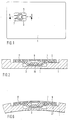
- FIG. 2 shows a cross section along the line A - A shown in FIG. 1.
- the electronic module 3 can be divided into two areas, namely a central area and an outer area.
- the integrated circuit 9 is applied in the central area and e.g. connected to the contact surfaces 5 by means of bonding wires 11.
- the integrated circuit 9 and the bond wires 11 are cast with a casting compound 15.
- the central area thus contains the sensitive components of the electronic module 3 (namely the integrated circuit and the conductive connections from the circuit to the contact surfaces) and is relatively rigid.
- the outer area of the module 3 consists exclusively of the thin metal layer and serves to connect the module to the data carrier.
- an adhesive layer 17 is applied, with the aid of which the electronic module 3, as shown in FIG. 2, is glued into a recess in the data carrier.
- the adhesive layer 17 projects partially onto the casting compound 15 and seals the recess in which the module 3 is located from the outside.
- no air can penetrate into the recess.
- the rigid central area is largely mechanically decoupled from the outer area, which in the exemplary embodiment shown occurs through windows 7 located in the outer area.
- a very good decoupling is guaranteed if the windows are as close as possible to the central area.
- the electronic module is glued into the recess of a data carrier provided.
- This installation technique is generally referred to as assembly technique.
- the module can also be used in another way in the card body of the data carrier, e.g. by inserting the module into a layer structure and connecting the layers under the action of heat and pressure (laminating technology) or by inserting the module into an injection mold and producing the data carrier by injecting plastic material into the mold cavity of the mold (injection molding technology).
- the relief areas of the module (designed as window 7 in FIG. 2) remain largely free of material of the data carrier. Filling the relief areas with material from the data carrier would counteract the mechanical decoupling of the two areas of the module.
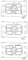
- 3 to 5 each show a metal strip with a contact layout in supervision.
- contact layouts are first produced at equidistant intervals, for example by punching or etching, etc., which initially remain connected to the metal strip via webs 19.
- the contact layout is preferred designed so that the part 13 of the contact surfaces 5, which lies on the casting compound in the central area in the finished module, is as large as possible so that a good bond between this part of the contact surfaces and the casting compound is ensured.
- the cross-sectional area of the contact areas 5 is reduced in the outer area. This is preferably done in the immediate vicinity of the central area, which is indicated by dashed lines in FIGS. 3 to 5, since a particularly good mechanical decoupling of the areas is then achieved.
- the cross-sectional area is reduced by introducing windows 7 into the contact areas 5, which have already been explained in connection with FIGS. 1 and 2.
- the corresponding area is perforated, as is indicated by the perforation holes 21.
- the cross-sectional area is reduced by bays 23 which extend from the interruptions between the contact areas 5 into them, so that only one between the outer part and the part 13 of the contact areas which lies in the central region narrow bridge remains.
- FIG. 3 and 4 show, in addition to the windows 7 and / or the perforations 21, additional windows 25 which do not necessarily have to be present and whose function is explained in connection with FIG. 7.
- FIG. 6 shows a cross section along the line A - A shown in FIG. 1 through a data carrier with a leadframe module according to the invention, the data carrier being subjected to bending stress.
- the adhesive layer 17 can be designed to be flexible. This can e.g. with a paper fleece that is soaked in thermally activated glue. The flexibility of the adhesive layer 17 leads to the fact that bending forces acting on the shoulder 27 are absorbed by the adhesive layer 17, which leads to a shearing of the adhesive layer 17, as is indicated in FIG. 6. This relieves the central area of the module.
- the adhesive layer 17 can be a layer of flexible material that is impregnated with an adhesive (for example pressure-sensitive adhesive or thermally activated adhesive).
- the flexible material can be, for example, a paper fleece or else polyurethane foam.
- the adhesive layer 17 can have a second layer consisting of a second adhesive. The first and the second adhesive are then selected so that one of the two connects optimally to the electronic module and the other connects optimally to the data carrier.
- Such a two-layer adhesive layer 17 could look as follows, for example.
- the layer made of flexible material is soaked with a pressure sensitive adhesive.
- An additional layer of thermo-activatable adhesive is arranged on this layer, which over the Pressure sensitive adhesive of the first layer is glued to the first layer.
- the two-layer adhesive layer 17 designed in this way is arranged in the data carrier in such a way that the layer of flexible material soaked in adhesive is glued to the data carrier, while the layer of thermally activatable adhesive is bonded to the contact surfaces 5 of the electronic module.
- An additional relief of the central area can also be achieved in that the relief areas of the electronic module (ie the areas in which the windows 7, perforations etc. are located) are not underlaid by an adhesive layer.
- This can be achieved, for example, by producing a window so large in the adhesive layer 17 that both the central area of the electronic module and the relief areas lie therein, as shown in FIG. 10.
- an adhesive layer prepared in this way can also be designed to be flexible.
- Fig. 7 shows an electronic module 3 in a mold, which consists of two halves 29 and 31.
- the module 3 is cast with a casting compound, which can be done either by casting or by injection molding.
- the mold half 29 contains projections 33 which engage in the additional windows 25 (see, for example, FIG. 3) and seal the mold cavity accordingly.
- a magnet 35 can be introduced into the mold half 31, which is activated before the casting process and attracts the contact layout, which in this case consists of a magnetic metal or is coated with a magnetic material, and its flatness against the wall of the mold half 31 improved. In this way it can be largely prevented be that casting compound penetrates through the interruptions in the contact layout on the side of the contact layout opposite the circuit 9 and contaminates the external contact surfaces.
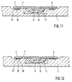
- FIG. 11 shows a further development of the data carrier according to FIGS. 1, 2, 6 and 10 in section.
- the difference between the data carrier according to FIG. 11 and the data carrier of FIGS. 1, 2, 6 and 10 can essentially be seen in the fact that the electronic module 3 is glued to the data carrier 1 via a liquid adhesive 36.
- the data carrier has means in the form of depressions 37, each of which is located within the contour of the individual contact surfaces 5 and thus have an all-round conversion.
- a drop of liquid adhesive 36 is poured into the recesses 37 and then the module 3 is inserted into the recess in the data carrier 1. Due to the recesses 37, the adhesive cannot escape.
- FIG. 12 shows a further development of the data carrier according to FIG. 11 in section.
- the data carrier differs from that of FIG. 11 in that the depressions 37 have additional ridges 38 in an inner region.
- the electronic module 3 and the data carrier 1 are glued over a thin film of the liquid adhesive 36, so that a better adhesive effect is achieved between the module and the data carrier.
- the excess adhesive can flow into the channel that is formed between the depressions 37 and the elevations 38.
Landscapes
- Engineering & Computer Science (AREA)
- Computer Hardware Design (AREA)
- Microelectronics & Electronic Packaging (AREA)
- Physics & Mathematics (AREA)
- General Physics & Mathematics (AREA)
- Theoretical Computer Science (AREA)
- Credit Cards Or The Like (AREA)
- Structures Or Materials For Encapsulating Or Coating Semiconductor Devices Or Solid State Devices (AREA)
- Lead Frames For Integrated Circuits (AREA)
- Mobile Radio Communication Systems (AREA)
Applications Claiming Priority (2)
| Application Number | Priority Date | Filing Date | Title |
|---|---|---|---|
| DE4443767 | 1994-12-08 | ||
| DE4443767A DE4443767A1 (de) | 1994-12-08 | 1994-12-08 | Elektronisches Modul und Datenträger mit elektrischem Modul |
Publications (3)
| Publication Number | Publication Date |
|---|---|
| EP0716394A2 true EP0716394A2 (fr) | 1996-06-12 |
| EP0716394A3 EP0716394A3 (fr) | 1997-07-16 |
| EP0716394B1 EP0716394B1 (fr) | 2001-07-04 |
Family
ID=6535315
Family Applications (1)
| Application Number | Title | Priority Date | Filing Date |
|---|---|---|---|
| EP95119306A Revoked EP0716394B1 (fr) | 1994-12-08 | 1995-12-07 | Module électronique et support d'information à module électronique |
Country Status (7)
| Country | Link |
|---|---|
| US (1) | US5834755A (fr) |
| EP (1) | EP0716394B1 (fr) |
| JP (1) | JP4140983B2 (fr) |
| AT (1) | ATE202866T1 (fr) |
| DE (2) | DE4443767A1 (fr) |
| DK (1) | DK0716394T3 (fr) |
| ES (1) | ES2158033T3 (fr) |
Cited By (6)
| Publication number | Priority date | Publication date | Assignee | Title |
|---|---|---|---|---|
| FR2751918A1 (fr) * | 1996-07-30 | 1998-02-06 | Solaic Sa | Carte a memoire, et procede de fabrication d'une telle carte |
| WO1998007113A1 (fr) * | 1996-08-08 | 1998-02-19 | Siemens Aktiengesellschaft | Carte a puce, procede de fabrication d'une carte a puce, et puce de semi-conducteur utilisable dans une carte a puce |
| WO1999060518A1 (fr) * | 1998-05-20 | 1999-11-25 | Bull Cp8 | Support pour un circuit electronique, comprenant des moyens anti-arrachement |
| EP1122685A1 (fr) * | 2000-02-02 | 2001-08-08 | Infineon Technologies AG | Carte à puce avec des points de pliage prédéfinis |
| EP1095356B1 (fr) * | 1999-05-14 | 2011-07-20 | Robert Bosch Gmbh | Agencement a contact et module a contact antagoniste |
| WO2012010682A1 (fr) * | 2010-07-23 | 2012-01-26 | Gemalto Sa | Module electronique securise, dispositif a module electronique securise et procede de fabrication |
Families Citing this family (34)
| Publication number | Priority date | Publication date | Assignee | Title |
|---|---|---|---|---|
| DE19512725C1 (de) * | 1995-04-05 | 1996-09-12 | Orga Kartensysteme Gmbh | Ausweiskarte o.dgl. in Form einer Chipkarte |
| US6072698A (en) * | 1995-09-27 | 2000-06-06 | Siemens Aktiengesellschaft | Chip module with heat insulation for incorporation into a chip card |
| DE19535989C3 (de) * | 1995-09-27 | 2003-03-27 | Siemens Ag | Chipmodul |
| FR2749687B1 (fr) * | 1996-06-07 | 1998-07-17 | Solaic Sa | Carte a memoire et procede de fabrication d'une telle carte |
| US6068191A (en) * | 1996-08-01 | 2000-05-30 | Siemens Aktiengesellschaft | Smart card with card body and semiconductor chip on a leadframe |
| DE19701163C2 (de) * | 1997-01-15 | 2001-12-06 | Siemens Ag | Elektrische Schaltung insbesondere für eine Chipkarte |
| DE19732915C1 (de) | 1997-07-30 | 1998-12-10 | Siemens Ag | Verfahren zur Herstellung eines Chipmoduls |
| DE19743409A1 (de) * | 1997-10-01 | 1999-04-08 | Bosch Gmbh Robert | Meßvorrichtung zur Messung der Masse eines strömenden Mediums |
| JP4179423B2 (ja) * | 1998-03-27 | 2008-11-12 | エヌエックスピー ビー ヴィ | 金属リードフレームに基づく埋め込みモジュールと二面チィプカバーを有するデータ媒体 |
| EP0998725A1 (fr) * | 1998-03-27 | 2000-05-10 | Koninklijke Philips Electronics N.V. | Support de donnees avec module implante sur la base d'un reseau de connexions metallique |
| FR2779851B1 (fr) * | 1998-06-12 | 2002-11-29 | Gemplus Card Int | Procede de fabrication d'une carte a circuit integre et carte obtenue |
| FR2788882A1 (fr) * | 1999-01-27 | 2000-07-28 | Schlumberger Systems & Service | Dispositif a circuits integres, module electronique pour carte a puce utilisant le dispositif et procede de fabrication dudit dispositif |
| US6179210B1 (en) * | 1999-02-09 | 2001-01-30 | Motorola, Inc. | Punch out pattern for hot melt tape used in smartcards |
| FR2793330B1 (fr) * | 1999-05-06 | 2001-08-10 | Oberthur Card Systems Sas | Procede de montage d'un microcircuit dans une cavite d'une carte formant support et carte ainsi obtenue |
| DE10101280A1 (de) * | 2001-01-12 | 2002-07-25 | Infineon Technologies Ag | Chipträger für Chipmodul |
| US6910635B1 (en) * | 2002-10-08 | 2005-06-28 | Amkor Technology, Inc. | Die down multi-media card and method of making same |
| JP4437014B2 (ja) * | 2003-04-25 | 2010-03-24 | パナソニック株式会社 | 電子回路装置 |
| US20060146271A1 (en) * | 2005-01-04 | 2006-07-06 | Pennaz Thomas J | Universal display module |
| US7599192B2 (en) * | 2005-04-11 | 2009-10-06 | Aveso, Inc. | Layered structure with printed elements |
| US7821794B2 (en) * | 2005-04-11 | 2010-10-26 | Aveso, Inc. | Layered label structure with timer |
| JP4736557B2 (ja) * | 2005-06-15 | 2011-07-27 | 大日本印刷株式会社 | Icカード用icモジュールとその製造方法 |
| ATE431601T1 (de) * | 2005-12-30 | 2009-05-15 | Incard Sa | Modul einer ic-karte |
| DE602005013807D1 (de) * | 2005-12-30 | 2009-05-20 | Incard Sa | IC Karte mit verbesserter Leiterplatine |
| DE102006028815B3 (de) * | 2006-06-21 | 2007-08-30 | Hansa Tronic Gmbh | Verfahren zur Herstellung eines elektrischen Hybridbauteils |
| USD686214S1 (en) * | 2011-07-28 | 2013-07-16 | Lifenexus, Inc. | Smartcard with iChip contact pad |
| USD711842S1 (en) * | 2011-08-04 | 2014-08-26 | Swisscom Ag | Electronic chip card |
| US8649820B2 (en) | 2011-11-07 | 2014-02-11 | Blackberry Limited | Universal integrated circuit card apparatus and related methods |
| US8936199B2 (en) | 2012-04-13 | 2015-01-20 | Blackberry Limited | UICC apparatus and related methods |
| USD703208S1 (en) | 2012-04-13 | 2014-04-22 | Blackberry Limited | UICC apparatus |
| USD701864S1 (en) | 2012-04-23 | 2014-04-01 | Blackberry Limited | UICC apparatus |
| USD707682S1 (en) * | 2012-12-05 | 2014-06-24 | Logomotion, S.R.O. | Memory card |
| FR2999112B1 (fr) * | 2012-12-12 | 2015-02-06 | Oberthur Technologies | Plaque de lamination a structure double plaque |
| CN107111767B (zh) * | 2014-12-23 | 2020-11-20 | 3M创新有限公司 | 柔性射频识别标签 |
| US10817768B1 (en) | 2019-12-20 | 2020-10-27 | Capital One Services, Llc | Systems and methods for preventing chip fraud by inserts in chip pocket |
Family Cites Families (18)
| Publication number | Priority date | Publication date | Assignee | Title |
|---|---|---|---|---|
| DE3131216C3 (de) * | 1981-04-14 | 1994-09-01 | Gao Ges Automation Org | Ausweiskarte mit IC-Baustein |
| DE3248385A1 (de) * | 1982-12-28 | 1984-06-28 | GAO Gesellschaft für Automation und Organisation mbH, 8000 München | Ausweiskarte mit integriertem schaltkreis |
| JPS6175986A (ja) * | 1984-09-21 | 1986-04-18 | Tokyo Jiki Insatsu Kk | 集積回路素子装着媒体 |
| US4586379A (en) * | 1984-09-28 | 1986-05-06 | Virginia Corporation Of Richmond | Ultrasonic pipe inspection system |
| FR2579799B1 (fr) * | 1985-03-28 | 1990-06-22 | Flonic Sa | Procede de fabrication de cartes a memoire electronique et cartes obtenues suivant ledit procede |
| DE3689094T2 (de) * | 1985-07-27 | 1994-03-10 | Dainippon Printing Co Ltd | IC-Karte. |
| JPS62214998A (ja) * | 1986-03-17 | 1987-09-21 | 三菱電機株式会社 | 薄型半導体カ−ド |
| DE3639630A1 (de) * | 1986-11-20 | 1988-06-01 | Gao Ges Automation Org | Datentraeger mit integriertem schaltkreis und verfahren zur herstellung desselben |
| DE3723547C2 (de) * | 1987-07-16 | 1996-09-26 | Gao Ges Automation Org | Trägerelement zum Einbau in Ausweiskarten |
| FR2629236B1 (fr) * | 1988-03-22 | 1991-09-27 | Schlumberger Ind Sa | Procede de realisation d'une carte a memoire electronique et carte telle qu'obtenue par la mise en oeuvre dudit procede |
| US5208450A (en) * | 1988-04-20 | 1993-05-04 | Matsushita Electric Industrial Co., Ltd. | IC card and a method for the manufacture of the same |
| FR2632100B1 (fr) * | 1988-05-25 | 1992-02-21 | Schlumberger Ind Sa | Procede de realisation d'une carte a memoire electronique et cartes a memoire electronique obtenue par la mise en oeuvre dudit procede |
| JPH0230598A (ja) * | 1988-07-20 | 1990-01-31 | Dainippon Printing Co Ltd | Icモジュールおよびicカード |
| FR2639763B1 (fr) * | 1988-11-29 | 1992-12-24 | Schlumberger Ind Sa | Procede de realisation d'un module electronique et module electronique tel qu'obtenu par ce procede |
| JPH04255260A (ja) * | 1991-02-07 | 1992-09-10 | Fujitsu Ltd | リードフレーム及び半導体装置の製造方法 |
| DE9110057U1 (de) * | 1991-08-14 | 1992-02-20 | Orga Kartensysteme GmbH, 6072 Dreieich | Datenträgerkarte mit eingeklebtem Schaltkreisträger |
| CH686325A5 (de) * | 1992-11-27 | 1996-02-29 | Esec Sempac Sa | Elektronikmodul und Chip-Karte. |
| JP3329073B2 (ja) * | 1993-06-04 | 2002-09-30 | セイコーエプソン株式会社 | 半導体装置およびその製造方法 |
-
1994
- 1994-12-08 DE DE4443767A patent/DE4443767A1/de not_active Withdrawn
-
1995
- 1995-12-05 US US08/567,458 patent/US5834755A/en not_active Expired - Fee Related
- 1995-12-07 DE DE59509381T patent/DE59509381D1/de not_active Revoked
- 1995-12-07 ES ES95119306T patent/ES2158033T3/es not_active Expired - Lifetime
- 1995-12-07 AT AT95119306T patent/ATE202866T1/de not_active IP Right Cessation
- 1995-12-07 DK DK95119306T patent/DK0716394T3/da active
- 1995-12-07 EP EP95119306A patent/EP0716394B1/fr not_active Revoked
- 1995-12-08 JP JP34579695A patent/JP4140983B2/ja not_active Expired - Fee Related
Cited By (13)
| Publication number | Priority date | Publication date | Assignee | Title |
|---|---|---|---|---|
| FR2751918A1 (fr) * | 1996-07-30 | 1998-02-06 | Solaic Sa | Carte a memoire, et procede de fabrication d'une telle carte |
| WO1998007113A1 (fr) * | 1996-08-08 | 1998-02-19 | Siemens Aktiengesellschaft | Carte a puce, procede de fabrication d'une carte a puce, et puce de semi-conducteur utilisable dans une carte a puce |
| US6188580B1 (en) | 1996-08-08 | 2001-02-13 | Infineon Technologies Ag | Smart card and semiconductor chip for use in a smart card |
| US6472733B1 (en) | 1998-05-20 | 2002-10-29 | Bull Cp8 | Electronic circuit support comprising tear resistant means |
| WO1999060518A1 (fr) * | 1998-05-20 | 1999-11-25 | Bull Cp8 | Support pour un circuit electronique, comprenant des moyens anti-arrachement |
| FR2778997A1 (fr) * | 1998-05-20 | 1999-11-26 | Bull Cp8 | Support pour un circuit electronique, comprenant des moyens anti-arrachement |
| EP1095356B1 (fr) * | 1999-05-14 | 2011-07-20 | Robert Bosch Gmbh | Agencement a contact et module a contact antagoniste |
| WO2001057793A1 (fr) * | 2000-02-02 | 2001-08-09 | Infineon Technologies Ag | Support de donnees portable |
| RU2234130C2 (ru) * | 2000-02-02 | 2004-08-10 | Инфинеон Текнолоджиз Аг | Носимый носитель данных |
| US6778407B2 (en) | 2000-02-02 | 2004-08-17 | Infineon Technologies Ag | Portable data carrier |
| EP1122685A1 (fr) * | 2000-02-02 | 2001-08-08 | Infineon Technologies AG | Carte à puce avec des points de pliage prédéfinis |
| WO2012010682A1 (fr) * | 2010-07-23 | 2012-01-26 | Gemalto Sa | Module electronique securise, dispositif a module electronique securise et procede de fabrication |
| EP2418608A1 (fr) * | 2010-07-23 | 2012-02-15 | Gemalto SA | Module électronique sécurisé, dispositif à module électronique sécurisé et procédé de fabrication |
Also Published As
| Publication number | Publication date |
|---|---|
| JP4140983B2 (ja) | 2008-08-27 |
| ATE202866T1 (de) | 2001-07-15 |
| US5834755A (en) | 1998-11-10 |
| ES2158033T3 (es) | 2001-09-01 |
| DK0716394T3 (da) | 2001-12-03 |
| EP0716394B1 (fr) | 2001-07-04 |
| DE4443767A1 (de) | 1996-06-13 |
| EP0716394A3 (fr) | 1997-07-16 |
| JPH0976680A (ja) | 1997-03-25 |
| DE59509381D1 (de) | 2001-08-09 |
Similar Documents
| Publication | Publication Date | Title |
|---|---|---|
| EP0716394B1 (fr) | Module électronique et support d'information à module électronique | |
| EP0756244B1 (fr) | Unité électronique et procédé de fabrication de cette unité | |
| EP0163880B1 (fr) | Support d'information à circuit intégré et procédé de fabrication d'un tel support | |
| EP0723244B1 (fr) | Support d'information à module électronique | |
| DE3122981C2 (fr) | ||
| EP0661666B1 (fr) | Méthode de fabrication d'une carte d'identité | |
| EP2566308B1 (fr) | Procédé d'équipement d'une plaquette | |
| DE2942397A1 (de) | Traegerband fuer elektronische schaltkreiselemente, verfahren zu seiner herstellung und anwendung bei einer signalverarbeitungseinrichtung | |
| DE68910385T3 (de) | Herstellungsverfahren einer elektronischen Speicherkarte und elektronische Speicherkarte, die nach diesem Verfahren hergestellt ist. | |
| EP0710919A2 (fr) | Module sans contact | |
| EP1028462A1 (fr) | Module électronique à type mince | |
| EP0521502B1 (fr) | Procédé pour l'installation d'un support | |
| EP0071255A2 (fr) | Carte portative pour le traitement d'informations | |
| DE102008019571A1 (de) | Chipkarte und Verfahren zu deren Herstellung | |
| EP0643366A2 (fr) | Module électronique de carte et production d'un tel module | |
| EP0757330A2 (fr) | Procédé de fabrication d'un support de données | |
| DE69905288T2 (de) | Verfahren zur herstellung einer kontaktlosen chipkarte | |
| WO2018019500A1 (fr) | Ensemble carte de circuit imprimé | |
| DE4040770A1 (de) | Datentraeger mit integriertem schaltkreis | |
| DE19633654A1 (de) | Elektronische Mikrogehäuse für eine elektronische Speicherkarte und Verfahren zur Herstellung derselben | |
| EP0655705A2 (fr) | Méthode de fabrication de cartes d'identités comportant des modules électroniques | |
| DE3138743A1 (de) | In einem dichten gehaeuse montiertes oberflaechenwellenfilter und dergleichen | |
| DE19526672A1 (de) | Datenträger mit integriertem Schaltkreis | |
| DE60036784T2 (de) | Integrierte schaltungsanordnung, elektronisches modul für chipkarte, das die anordnung benutzt, und verfahren zu deren herstellung | |
| EP1925192B1 (fr) | Substrat lamine destine au montage de composants electroniques |
Legal Events
| Date | Code | Title | Description |
|---|---|---|---|
| PUAI | Public reference made under article 153(3) epc to a published international application that has entered the european phase |
Free format text: ORIGINAL CODE: 0009012 |
|
| AK | Designated contracting states |
Kind code of ref document: A2 Designated state(s): AT BE CH DE DK ES FR GB GR IE IT LI LU MC NL PT SE |
|
| PUAL | Search report despatched |
Free format text: ORIGINAL CODE: 0009013 |
|
| AK | Designated contracting states |
Kind code of ref document: A3 Designated state(s): AT BE CH DE DK ES FR GB GR IE IT LI LU MC NL PT SE |
|
| 17P | Request for examination filed |
Effective date: 19971211 |
|
| 17Q | First examination report despatched |
Effective date: 19991123 |
|
| GRAG | Despatch of communication of intention to grant |
Free format text: ORIGINAL CODE: EPIDOS AGRA |
|
| GRAG | Despatch of communication of intention to grant |
Free format text: ORIGINAL CODE: EPIDOS AGRA |
|
| GRAH | Despatch of communication of intention to grant a patent |
Free format text: ORIGINAL CODE: EPIDOS IGRA |
|
| GRAH | Despatch of communication of intention to grant a patent |
Free format text: ORIGINAL CODE: EPIDOS IGRA |
|
| GRAA | (expected) grant |
Free format text: ORIGINAL CODE: 0009210 |
|
| AK | Designated contracting states |
Kind code of ref document: B1 Designated state(s): AT BE CH DE DK ES FR GB GR IE IT LI LU MC NL PT SE |
|
| PG25 | Lapsed in a contracting state [announced via postgrant information from national office to epo] |
Ref country code: GR Free format text: LAPSE BECAUSE OF NON-PAYMENT OF DUE FEES Effective date: 20010704 Ref country code: FR Free format text: LAPSE BECAUSE OF FAILURE TO SUBMIT A TRANSLATION OF THE DESCRIPTION OR TO PAY THE FEE WITHIN THE PRESCRIBED TIME-LIMIT Effective date: 20010704 |
|
| REF | Corresponds to: |
Ref document number: 202866 Country of ref document: AT Date of ref document: 20010715 Kind code of ref document: T |
|
| REG | Reference to a national code |
Ref country code: CH Ref legal event code: NV Representative=s name: PATENTANWAELTE SCHAAD, BALASS, MENZL & PARTNER AG Ref country code: CH Ref legal event code: EP |
|
| GBT | Gb: translation of ep patent filed (gb section 77(6)(a)/1977) |
Effective date: 20010706 |
|
| REG | Reference to a national code |
Ref country code: IE Ref legal event code: FG4D Free format text: GERMAN |
|
| REF | Corresponds to: |
Ref document number: 59509381 Country of ref document: DE Date of ref document: 20010809 |
|
| REG | Reference to a national code |
Ref country code: ES Ref legal event code: FG2A Ref document number: 2158033 Country of ref document: ES Kind code of ref document: T3 |
|
| ITF | It: translation for a ep patent filed | ||
| PG25 | Lapsed in a contracting state [announced via postgrant information from national office to epo] |
Ref country code: PT Free format text: LAPSE BECAUSE OF FAILURE TO SUBMIT A TRANSLATION OF THE DESCRIPTION OR TO PAY THE FEE WITHIN THE PRESCRIBED TIME-LIMIT Effective date: 20011004 |
|
| REG | Reference to a national code |
Ref country code: DK Ref legal event code: T3 |
|
| PG25 | Lapsed in a contracting state [announced via postgrant information from national office to epo] |
Ref country code: MC Free format text: LAPSE BECAUSE OF NON-PAYMENT OF DUE FEES Effective date: 20011207 Ref country code: LU Free format text: LAPSE BECAUSE OF NON-PAYMENT OF DUE FEES Effective date: 20011207 |
|
| EN | Fr: translation not filed | ||
| PG25 | Lapsed in a contracting state [announced via postgrant information from national office to epo] |
Ref country code: BE Free format text: LAPSE BECAUSE OF NON-PAYMENT OF DUE FEES Effective date: 20011231 |
|
| REG | Reference to a national code |
Ref country code: GB Ref legal event code: IF02 |
|
| PLBQ | Unpublished change to opponent data |
Free format text: ORIGINAL CODE: EPIDOS OPPO |
|
| PLBI | Opposition filed |
Free format text: ORIGINAL CODE: 0009260 |
|
| 26 | Opposition filed |
Opponent name: INFINEON TECHNOLOGIES AG Effective date: 20020218 |
|
| PLBF | Reply of patent proprietor to notice(s) of opposition |
Free format text: ORIGINAL CODE: EPIDOS OBSO |
|
| BERE | Be: lapsed |
Owner name: GIESECKE & DEVRIENT G.M.B.H. Effective date: 20011231 |
|
| NLR1 | Nl: opposition has been filed with the epo |
Opponent name: INFINEON TECHNOLOGIES AG |
|
| PLBF | Reply of patent proprietor to notice(s) of opposition |
Free format text: ORIGINAL CODE: EPIDOS OBSO |
|
| PGFP | Annual fee paid to national office [announced via postgrant information from national office to epo] |
Ref country code: DK Payment date: 20021227 Year of fee payment: 8 |
|
| PLAY | Examination report in opposition despatched + time limit |
Free format text: ORIGINAL CODE: EPIDOSNORE2 |
|
| PLBC | Reply to examination report in opposition received |
Free format text: ORIGINAL CODE: EPIDOSNORE3 |
|
| PG25 | Lapsed in a contracting state [announced via postgrant information from national office to epo] |
Ref country code: DK Free format text: LAPSE BECAUSE OF NON-PAYMENT OF DUE FEES Effective date: 20040102 |
|
| REG | Reference to a national code |
Ref country code: DK Ref legal event code: EBP |
|
| RDAF | Communication despatched that patent is revoked |
Free format text: ORIGINAL CODE: EPIDOSNREV1 |
|
| APBP | Date of receipt of notice of appeal recorded |
Free format text: ORIGINAL CODE: EPIDOSNNOA2O |
|
| APAH | Appeal reference modified |
Free format text: ORIGINAL CODE: EPIDOSCREFNO |
|
| APBQ | Date of receipt of statement of grounds of appeal recorded |
Free format text: ORIGINAL CODE: EPIDOSNNOA3O |
|
| APAH | Appeal reference modified |
Free format text: ORIGINAL CODE: EPIDOSCREFNO |
|
| PLAB | Opposition data, opponent's data or that of the opponent's representative modified |
Free format text: ORIGINAL CODE: 0009299OPPO |
|
| R26 | Opposition filed (corrected) |
Opponent name: INFINEON TECHNOLOGIES AG Effective date: 20020218 |
|
| PGFP | Annual fee paid to national office [announced via postgrant information from national office to epo] |
Ref country code: AT Payment date: 20061222 Year of fee payment: 12 |
|
| PGFP | Annual fee paid to national office [announced via postgrant information from national office to epo] |
Ref country code: SE Payment date: 20061227 Year of fee payment: 12 |
|
| PGFP | Annual fee paid to national office [announced via postgrant information from national office to epo] |
Ref country code: IT Payment date: 20061231 Year of fee payment: 12 |
|
| NLR1 | Nl: opposition has been filed with the epo |
Opponent name: INFINEON TECHNOLOGIES AG |
|
| PGFP | Annual fee paid to national office [announced via postgrant information from national office to epo] |
Ref country code: NL Payment date: 20071213 Year of fee payment: 13 Ref country code: ES Payment date: 20071220 Year of fee payment: 13 |
|
| PGFP | Annual fee paid to national office [announced via postgrant information from national office to epo] |
Ref country code: CH Payment date: 20071219 Year of fee payment: 13 |
|
| PGFP | Annual fee paid to national office [announced via postgrant information from national office to epo] |
Ref country code: GB Payment date: 20071220 Year of fee payment: 13 |
|
| PLAB | Opposition data, opponent's data or that of the opponent's representative modified |
Free format text: ORIGINAL CODE: 0009299OPPO |
|
| PGFP | Annual fee paid to national office [announced via postgrant information from national office to epo] |
Ref country code: DE Payment date: 20080227 Year of fee payment: 13 |
|
| R26 | Opposition filed (corrected) |
Opponent name: INFINEON TECHNOLOGIES AG Effective date: 20020218 |
|
| APBU | Appeal procedure closed |
Free format text: ORIGINAL CODE: EPIDOSNNOA9O |
|
| NLR1 | Nl: opposition has been filed with the epo |
Opponent name: INFINEON TECHNOLOGIES AG |
|
| RDAG | Patent revoked |
Free format text: ORIGINAL CODE: 0009271 |
|
| STAA | Information on the status of an ep patent application or granted ep patent |
Free format text: STATUS: PATENT REVOKED |
|
| REG | Reference to a national code |
Ref country code: CH Ref legal event code: PL |
|
| EUG | Se: european patent has lapsed | ||
| PG25 | Lapsed in a contracting state [announced via postgrant information from national office to epo] |
Ref country code: AT Free format text: LAPSE BECAUSE OF NON-PAYMENT OF DUE FEES Effective date: 20071207 |
|
| 27W | Patent revoked |
Effective date: 20080529 |
|
| GBPR | Gb: patent revoked under art. 102 of the ep convention designating the uk as contracting state |
Effective date: 20080529 |
|
| PG25 | Lapsed in a contracting state [announced via postgrant information from national office to epo] |
Ref country code: SE Free format text: LAPSE BECAUSE OF NON-PAYMENT OF DUE FEES Effective date: 20071208 |
|
| NLR2 | Nl: decision of opposition |
Effective date: 20080529 |
|
| PG25 | Lapsed in a contracting state [announced via postgrant information from national office to epo] |
Ref country code: IT Free format text: LAPSE BECAUSE OF NON-PAYMENT OF DUE FEES Effective date: 20071207 |
|
| PGFP | Annual fee paid to national office [announced via postgrant information from national office to epo] |
Ref country code: IE Payment date: 20071214 Year of fee payment: 13 |