EP1095356B1 - Agencement a contact et module a contact antagoniste - Google Patents
Agencement a contact et module a contact antagoniste Download PDFInfo
- Publication number
- EP1095356B1 EP1095356B1 EP00940179A EP00940179A EP1095356B1 EP 1095356 B1 EP1095356 B1 EP 1095356B1 EP 00940179 A EP00940179 A EP 00940179A EP 00940179 A EP00940179 A EP 00940179A EP 1095356 B1 EP1095356 B1 EP 1095356B1
- Authority
- EP
- European Patent Office
- Prior art keywords
- contact
- mating
- module
- smart card
- sub
- Prior art date
- Legal status (The legal status is an assumption and is not a legal conclusion. Google has not performed a legal analysis and makes no representation as to the accuracy of the status listed.)
- Expired - Lifetime
Links
Images


Classifications
-
- G—PHYSICS
- G06—COMPUTING OR CALCULATING; COUNTING
- G06K—GRAPHICAL DATA READING; PRESENTATION OF DATA; RECORD CARRIERS; HANDLING RECORD CARRIERS
- G06K19/00—Record carriers for use with machines and with at least a part designed to carry digital markings
- G06K19/06—Record carriers for use with machines and with at least a part designed to carry digital markings characterised by the kind of the digital marking, e.g. shape, nature, code
- G06K19/067—Record carriers with conductive marks, printed circuits or semiconductor circuit elements, e.g. credit or identity cards also with resonating or responding marks without active components
- G06K19/07—Record carriers with conductive marks, printed circuits or semiconductor circuit elements, e.g. credit or identity cards also with resonating or responding marks without active components with integrated circuit chips
- G06K19/077—Constructional details, e.g. mounting of circuits in the carrier
- G06K19/07745—Mounting details of integrated circuit chips
- G06K19/07747—Mounting details of integrated circuit chips at least one of the integrated circuit chips being mounted as a module
-
- G—PHYSICS
- G06—COMPUTING OR CALCULATING; COUNTING
- G06K—GRAPHICAL DATA READING; PRESENTATION OF DATA; RECORD CARRIERS; HANDLING RECORD CARRIERS
- G06K19/00—Record carriers for use with machines and with at least a part designed to carry digital markings
- G06K19/06—Record carriers for use with machines and with at least a part designed to carry digital markings characterised by the kind of the digital marking, e.g. shape, nature, code
- G06K19/067—Record carriers with conductive marks, printed circuits or semiconductor circuit elements, e.g. credit or identity cards also with resonating or responding marks without active components
- G06K19/07—Record carriers with conductive marks, printed circuits or semiconductor circuit elements, e.g. credit or identity cards also with resonating or responding marks without active components with integrated circuit chips
- G06K19/077—Constructional details, e.g. mounting of circuits in the carrier
- G06K19/07737—Constructional details, e.g. mounting of circuits in the carrier the record carrier consisting of two or more mechanically separable parts
- G06K19/07739—Constructional details, e.g. mounting of circuits in the carrier the record carrier consisting of two or more mechanically separable parts comprising a first part capable of functioning as a record carrier on its own and a second part being only functional as a form factor changing part, e.g. SIM cards type ID 0001, removably attached to a regular smart card form factor
-
- G—PHYSICS
- G06—COMPUTING OR CALCULATING; COUNTING
- G06K—GRAPHICAL DATA READING; PRESENTATION OF DATA; RECORD CARRIERS; HANDLING RECORD CARRIERS
- G06K19/00—Record carriers for use with machines and with at least a part designed to carry digital markings
- G06K19/06—Record carriers for use with machines and with at least a part designed to carry digital markings characterised by the kind of the digital marking, e.g. shape, nature, code
- G06K19/067—Record carriers with conductive marks, printed circuits or semiconductor circuit elements, e.g. credit or identity cards also with resonating or responding marks without active components
- G06K19/07—Record carriers with conductive marks, printed circuits or semiconductor circuit elements, e.g. credit or identity cards also with resonating or responding marks without active components with integrated circuit chips
- G06K19/077—Constructional details, e.g. mounting of circuits in the carrier
- G06K19/07743—External electrical contacts
-
- G—PHYSICS
- G06—COMPUTING OR CALCULATING; COUNTING
- G06K—GRAPHICAL DATA READING; PRESENTATION OF DATA; RECORD CARRIERS; HANDLING RECORD CARRIERS
- G06K7/00—Methods or arrangements for sensing record carriers, e.g. for reading patterns
- G06K7/0004—Hybrid readers
-
- G—PHYSICS
- G06—COMPUTING OR CALCULATING; COUNTING
- G06K—GRAPHICAL DATA READING; PRESENTATION OF DATA; RECORD CARRIERS; HANDLING RECORD CARRIERS
- G06K7/00—Methods or arrangements for sensing record carriers, e.g. for reading patterns
- G06K7/0013—Methods or arrangements for sensing record carriers, e.g. for reading patterns by galvanic contacts, e.g. card connectors for ISO-7816 compliant smart cards or memory cards, e.g. SD card readers
- G06K7/0021—Methods or arrangements for sensing record carriers, e.g. for reading patterns by galvanic contacts, e.g. card connectors for ISO-7816 compliant smart cards or memory cards, e.g. SD card readers for reading/sensing record carriers having surface contacts
-
- Y—GENERAL TAGGING OF NEW TECHNOLOGICAL DEVELOPMENTS; GENERAL TAGGING OF CROSS-SECTIONAL TECHNOLOGIES SPANNING OVER SEVERAL SECTIONS OF THE IPC; TECHNICAL SUBJECTS COVERED BY FORMER USPC CROSS-REFERENCE ART COLLECTIONS [XRACs] AND DIGESTS
- Y10—TECHNICAL SUBJECTS COVERED BY FORMER USPC
- Y10S—TECHNICAL SUBJECTS COVERED BY FORMER USPC CROSS-REFERENCE ART COLLECTIONS [XRACs] AND DIGESTS
- Y10S439/00—Electrical connectors
- Y10S439/946—Memory card cartridge
-
- Y—GENERAL TAGGING OF NEW TECHNOLOGICAL DEVELOPMENTS; GENERAL TAGGING OF CROSS-SECTIONAL TECHNOLOGIES SPANNING OVER SEVERAL SECTIONS OF THE IPC; TECHNICAL SUBJECTS COVERED BY FORMER USPC CROSS-REFERENCE ART COLLECTIONS [XRACs] AND DIGESTS
- Y10—TECHNICAL SUBJECTS COVERED BY FORMER USPC
- Y10S—TECHNICAL SUBJECTS COVERED BY FORMER USPC CROSS-REFERENCE ART COLLECTIONS [XRACs] AND DIGESTS
- Y10S439/00—Electrical connectors
- Y10S439/948—Contact or connector with insertion depth limiter
Definitions
- the invention is based on an electrically contactable contact module and a mating contact module according to the independent claims.
- electrically contactable modules Arranged on card-shaped carriers, electrically contactable modules have long been known in the form of so-called smart cards, such as telephone, Eurocheque, health insurance cards or as so-called key cards for car radios from Blauddling-Werke GmbH. These consist essentially of at least one embedded in a plastic card given dimensions microchip, which can be designed as a memory and / or microprocessor chip.
- smart cards according to the standard ISO 7816-1 and following, the contacts of a microchip embedded in the card are connected to arranged on the surface of the card contact surfaces.
- the module embedded in the plastic card can thus be contacted for reading out its information or for exchanging information between the module and the chip card reader.
- a chip card known.
- a chip is arranged on a card-shaped carrier.
- the chip has a plurality of contacts.
- the EP 0 716 394 A2 shows a similar chip card. These smart cards can only be read with mating contacts designed for this contact arrangement. If a card with a different contact surface arrangement is inserted in this reader, it can not read the other card.
- the FR 2 634 095 shows a contact surface arrangement with two contact areas, which are electrically connected to each other. If a universal reader for smart cards to be created, this contact arrangement for reading different smart cards is not suitable.
- EP 1 147 486 and WO 00/42568 are relevant under Art. 54 (3) EPC and disclose in Fig. 4, 5 and 6 a chip card with a contact arrangement, in which two contact fields are interconnected within and outside a predetermined range.
- the invention enables, for example, the contacting and evaluation of or communication with said multi-media cards by means of a chip card reader provided for smart cards according to the standard ISO 7816-1 and following.
- the invention makes it possible to contact the aforementioned multi-media cards both with an ISO 7816 chip card reader and with a chip card reader provided for multi-media cards, since the invention allows the adaptation of the contact surfaces of the MMC card to the ISO 7816 chip card reader. Standard while maintaining the MMC contact surface arrangement permits.
- An inventive mating contact module is formed in an advantageous manner for contacting a contact arrangement according to the invention by a corresponding arrangement of its mating contacts.
- Such a mating contact module can be produced in a simple manner from a conventional mating contact module for contacting, for example, ISO-7816 contact arrangements by arranging a further mating contact part module.
- An advantageous embodiment of means for cascading the mating contact part modules constitute a dovetail-shaped groove milled into a side wall of the mating contact part module, and a dovetail-shaped spring formed on a correspondingly opposite side wall of the mating contact element module to be marked Arranging means are on a side wall of the mating contact module, so for example, an ISO 7816 mating contact module molded dowel pins which engage in mating holes in an opposite side wall of the mating counter contact part module.
- At least one arranged on the top and / or bottom of the mating contact module module locking hook which engages in at least one corresponding recess in the top and / or bottom of a bayed another Jacobkeymoduls allows fixation and stabilization of a Jacobumbleteilmodulen constructed mating contact module and thus the position of the contact rows and the contact distances to each other.
- a mating contact part module On the top of a mating contact part module arranged means for latching mounting of mating contact elements, for example in the form of latching hooks in conjunction with locking lugs allow easy retrofitting of individual mating contact elements at the same time secure and poition-accurate fixation used mating contact elements.
- Chip cards within the meaning of ISO standard 7816 belong to the group of identification cards as defined in the ISO 7810 "Identification Cards - Physical Characteristics" standard. This standard specifies the physical characteristics of identification cards including material properties such as flexibility, temperature resistance and dimensions for three different sizes of cards (ID-1, ID-2 and ID-3).
- the basis for the chip card standards ISO 7816-1 and following forms the ID-1-96, as today often as a card for the payment traffic, z. B. is spread as a credit or Eurocheque card.
- Such a chip card contains an integrated circuit in the card body, which has elements for data transmission, for storing data and for processing data.
- the data transmission can take place either via the contacts on the surface of the card, or contactless by electromagnetic fields.
- FIG. 1 shows a section of a chip card 100 according to ISO 7816 in plan view.
- This has a, relative to the insertion direction 110, front edge 130 and a, designated in ISO 7816 as an upper edge, right edge 120, wherein the position of the contact surfaces 101, 102, 103, 104, 105, 106, 107 and 108th that on the top the chip card are accessible from the outside, is specified in the ISO 7816-2 with respect to the edges 120 and 130.
- ISO 7816-2 specifies minimum dimensions of contact surfaces 101 to 108 of 1.7 mm x 2.0 mm.
- the distances 131 of the contact surfaces 101 to 108 from the front edge and the distances 121 of the contact surfaces from the top edge represent maximum dimensions, the distances 132 from the front edge and 122 from the top edge minimum dimensions.
- the maximum distances 131 of the contact surfaces 101 to 104 and the minimum distances 132 of the contact surfaces 105 to 108 from the leading edge of the chip card and the maximum distances 121 of the contact surfaces 101 and 105 and the minimum distances 122 of the contact surfaces 104 and 108 of the Top edge of the chip card 100 defines a rectangular area 150 of 9.62 mm x 9.32 mm, according to ISO 7816, the contact surfaces 10I to 108 must at least occupy.
- the region 150 is also referred to as a predetermined region in the context of the present invention. ISO 7816-2 allows the contact surfaces to protrude beyond the specified range.
- Two adjacent rows of contacts (contact surfaces 101 to 104 and 105 to 108) provided in the insertion direction 110 have a center distance 139 of 7.62 mm, the center distance 129 of two adjacent contact surfaces 101 and 102 transverse to the insertion direction 110 being 2.54 mm.
- the Eurocheque card shown in FIG. 1 has its contact pad 151, which is composed of the contacts 101 to 108, having an area of approximately 11.7 mm (153) in the insertion direction and approximately 10.5 mm (152) transversely to the insertion direction.
- the distances 131 of the contact surfaces 101 to 104 to the leading edge and 121 of the contact surfaces 101 and 105 to the upper edge are approximately 9.0 mm and 18.5 mm.
- the outer dimensions of the illustrated Eurocheque card in the ID-1 format which contains a magnetic strip 160 on its rear side as an additional storage medium, amount to approximately 85.5 mm (111) in the insertion direction and approximately 54.0 mm (112) across.
- a different from the standard 7816 chip card provides the in FIG. 3 presented multi-media card 200, short MMC, the company Siemens.
- a standard chip card is the chip carrier with the actual chip formed as a unit, on the surface of the contact surfaces for contacting the chip are arranged.
- the chip carrier is likewise glued, as in a standard chip card, into a corresponding recess in the card 200 in such a way that the surface of the chip carrier is flush with that of the MMC card 200 and the contact surfaces are at the top of the card.
- the contact field of the MMC card which is referred to below as the first contact field, has a distance 231 of 1.0 mm in the form of a first contact row with contact surfaces 201, 202, 203, 204, 205, 206 and 207 running to the narrow front side 230 of the chip card.
- the contact surfaces 201 to 207 themselves have dimensions of 1.7 mm (221) x 3.5 mm (231) and have a distance of 0.625 mm from each other transversely to the broad side 220 of the MMC card.
- FIG. 4 the overlapping projection of the contact pads of a chip card according to ISO 7816 and the MMC card, can easily be seen, both the contact surfaces 101 to 108 of the ISO 7816 chip card, and the contact surfaces 201 to 204 of the MMC card within the dimensions of the given Area 150.
- the contacts 201 to 204 of the MMC card do not meet the requirements of the standard ISO 7816-2, they can be adapted to the ISO 7816-2 standard by slight widening.
- the contact surfaces 205 to 207 of the MMC card are outside the predetermined range 150.
- a corresponding inventive arrangement, realized for example on an MMC card shows FIG. 5 .
- the contact arrangement of FIG. 5 comprises a contact pad with contacts 301 to 304, which result from a superimposition of the contact surfaces 101 to 104 according to ISO 7816-2 and 201 to 204 of the MMC card, and those in the range specified by ISO 7816-2 area 150 both the requirements of ISO 7816-2, as well as the requirements for MMC card contact surfaces. Furthermore, a contact field with contact surfaces 305 to 308 is provided, which likewise meets the requirements of ISO 7816-2 with respect to their position. The lying outside the predetermined range 150 contact surfaces 205, 206 and 207 of the MMC card are taken over unchanged (contact surfaces 315, 316 and 317) and thus allow furthermore, the evaluation of the MMC card by means of an MMC card reader.
- the conductor tracks are guided along the surface of the chip card 200 or of the chip carrier.
- the embodiment described above relates to a modified contact arrangement for MMC modules.
- contact arrangement for example, on a chip card to ISO 7816 provide.
- an ISO 7816 chip card can also be evaluated for ISO 7816 chip card readers as well as MMC card readers.
- the invention is not limited to the production of compatibility between the ISO 7816 standard and MMC. Rather, the invention makes it possible, by suitable arrangement of a second contact field within a range specified by a standard, such as, for example, ISO 7816, to adapt different contact arrangements to the standard.
- a restriction arises at best by different numbers of contacts, that is, for example, when the adapted contact arrangement has more occupied contacts than the standard contact arrangement.
- FIG. 6 shows by way of example a mating contact module 400 with mating contacts 401 to 408 and 415 to 417 against the background of a contact arrangement 300 according to the invention, which is adapted for alternative evaluation by means of an ISO 7816 or an MMC chip card reader.
- Each contact surface 301 to 308 of the ISO 7816 contact field is assigned its own mating contact 401, 402, 403, 404, 405, 406, 407 and 408 of the mating contact module 400.
- the mating contact module 400 also has further contacts 415, 416 and 417 which are associated with the contact surfaces 315, 316 and 317 of the MMC contact field.
- the mating contacts 401 to 408 and 415 to 417 are embodied in the form of metallic leaf springs, which have contact beads 410 for contacting the contact surfaces 301 to 308 and 315 to 317 on their undersides which are facing the contact surfaces.
- the mating contacts are mounted in a carrier, in the present case in a frame-shaped plastic carrier 430.
- 430 tracks are laid in the frame, which establish an electrical connection between the mating contacts and a connector.
- the described mating contact module is thus suitable for use in a chip card reader for the alternative evaluation of chip cards with different contact fields, for example from ISO 7816-, as well as MMC chip cards suitable.
- a mating contact module is in the FIGS. 7 and 8 shown.
- the mating contact module 400 in this case consists of subassemblies 450 and 460 that can be arranged on one another.
- the submodules 450 and 460 have essentially cuboidal bodies with a top side 451 and side faces 453, 454, 455 and 456. From the upper side 451 of the first submodule 450 protrude two mating contact rows with mating contacts 401 to 408 for contacting the contact surfaces of an ISO 7816 chip card, their arrangement to each other to meet the requirements of ISO 7816.
- the mating contacts 401 to 404 are connected to solder terminals 421, 422, 423, 424, which are led out of parallel to the first mating contact row 401 to 404 side wall 453.
- the second sub-module 460 has, like the first sub-module 450, mating contacts 415, 416 and 417 for contacting the further contact surfaces 205, 206 and 207 of an MMC module or 315, 316 and 317 of an adapted to the MMC format contact arrangement of an ISO-7816 Chip card on. These are just as with the first sub-module, with the first side surface 453 of the Mating contact module body lead out terminals 425, 426 and 427 connected.
- a third side wall 455 and a fourth side wall 456 of the cuboid mating contact module body have means for juxtaposing mating contact modules, for example, complementing the first mating contact module 450 by a second mating contact module 460 to form a mating contact module 400 for contacting both ISO 7816 smart cards and MMC Cards, up.
- the first submodule has on its third side face another dovetail spring 457, the second submodule 460 on its fourth side face 456 a further dovetail groove 458.
- the dimensions of the sub-module body in particular the position of the mating contacts 401 to 408 and 415 to 417 relative to the third and fourth side surface, are dimensioned so that a mated to the fourth side surface 456 of the first sub-module 450 second sub-module 460 formed mating contact module 400 for contacting both ISO-7816 contact arrangements, as well as MMC contact arrangements is suitable, in particular the predetermined by the ISO 7816 and the MMC standard contact distances are met.
- FIG. 8 shows a section through the first mating contact part module 450.
- the mating contact 401 is, like the other mating contacts 402 to 408 and also the mating contacts 415 to 417 of the second sub-module 460, designed in the form of a spring-mounted pin.
- the tip of the mating contact 401 is rounded to substantially wear and damage-free contacting an associated contact surface 101 or 301, or, as in the present case, designed in the form of a hemisphere.
- a ring 431 is formed, which is guided in a groove 432 of the mating contact module body.
- the arrangement of ring 431 and groove 432 allows movement of the pin in the direction perpendicular to the module top 451 direction and prevents falling out of the counter contact pin 401 from the mating contact module 450.
- a metallic coil spring 433 in the direction of the top 451 of the mating contact module 450.
- the maximum deflection of the pin 401 is limited by the upper cover of the groove 432.
- the lower abutment of the spiral spring 433 forms the led out of the mating contact module body solder terminal 421st
- the mating contact module 450 is exemplified as an SMD (surface mounted device) component for solder mounting on the surface of a circuit board 440.
- SMD surface mounted device
- the mating contact arrangement for making contact with an inventive, an ISO-7816 or an MMC contact arrangement can also be realized in the form of contact holder which can be freely fitted with mating contacts as required.
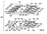
- FIG. 9 A third variant of a mating contact module 400 for contacting both ISO 7816 chip cards and MMC cards is in FIG. 9 shown.
- the mating contact module consists of two parallelepiped, lined up with each other sub-modules 450 and 460, which are constructed substantially the same and differ only in the number of mating contacts 401 to 408 and 415-417, or can be arranged on the module body mating contacts.
- the sub-modules 450 and 460 For juxtaposing the sub-modules 450 and 460, these have at their third and fourth side surface, which are perpendicular to the contact rows and the first and second side walls 453 and 454, alignment means in the form of holes 461 on the third side wall 453 and dowels 462 on the fourth side wall 454 on.
- the dowels 462 effect in conjunction with the mating holes 461 for receiving the dowels when juxtaposing the sub-modules 450 and 460 their mutual alignment, so that the surfaces 451 and the first and second side surfaces of the sub-modules 450 and 460 are aligned, so in each case a common area form.
- the means for juxtaposing the sub-modules comprise means for interlocking the cascaded sub-modules 450 and 460 among themselves. These are in the form of a respective arranged on the upper side 451 of the sub-modules 450 and 460 locking hook 465 which projects beyond the body of the respective sub-module in the direction of the third side surface 455, and aligned with one another and perpendicular to the first and second side walls 453 and 454 to each other Part modules engages in a recess 464 in the surface 451 of the respective adjacent sub-module 460. In this way, the two adjacent sub-modules 450 and 460 are locked against each other by the locking means 464 and 465. The distances of the contacts 415 and 404 to each other are thus fixed.
- the sub-modules have at their upper edges along the first and second side surfaces 453 and 454 recesses 469 for receiving mating contact elements 481. Further, means 467, 468 are arranged for latching mounting of the mating contact elements 481 on the top of the sub-modules.
- the mounting means further comprise a latching nose 468, which is disposed immediately adjacent to the latching hook 467 on its open side on the surface 451 of the module body.
- the Locking lug is either on the underside of the first leg of the latching hook 468, or, as in the present embodiment, arranged on the surface 451 of the module body. Latching hook 467 and locking lug 468 thus form a channel 470, in which a mating contact element 481 can be inserted latching.
- the height of the detent is preferably opposite to the predetermined by the thickness of the mating contact element 181 height of the second leg 467 b of the latching hook 467 low, so that by slight bending of the latching hook 467 a mating contact element on the latching nose is inserted into the opening of the latching hook. At the same time, the height of the detent 468 is large enough, so that unintentional sliding out of the mating contact element 481 is avoided from the latching hook.
- the mating contact elements 481 are designed in the form of bent metallic spring strips made of a material with good electrical conductivity. In the area of the contact surfaces of the module to be contacted, they have a semicircular bulge which serves as mating contact 401. Towards the edge of the module body 450, the spring strips are bent downwards, that is to say to the bottom surface 452 of the module body, where they pass into connections 421, in the present case for SMD circuit board assembly.
- the module body can also be designed without the latching means 467, 468 for the mating contact elements 481 and then serves, for example, merely as a positioning aid in the assembly of the mating contact elements 481 according to the provisions applicable to the contact arrangement according to the invention and to support the mating contact elements 481 against a chip to be evaluated or MMC card on the mating contacts 401 applied pressure force.
Landscapes
- Engineering & Computer Science (AREA)
- Computer Hardware Design (AREA)
- Microelectronics & Electronic Packaging (AREA)
- Physics & Mathematics (AREA)
- General Physics & Mathematics (AREA)
- Theoretical Computer Science (AREA)
- Artificial Intelligence (AREA)
- Computer Vision & Pattern Recognition (AREA)
- Credit Cards Or The Like (AREA)
- Coupling Device And Connection With Printed Circuit (AREA)
Abstract
Claims (14)
- Carte à puce dotée d'un support en forme de carte et d'un système de surfaces de contact disposé sur le support en forme de carte et doté d'une micropuce incorporée dans le support et de surfaces de contact reliées à la micropuce,
le système de surfaces de contact présentant une première zone de contact qui comprend plusieurs surfaces de contact (101 - 108) et qui est située à l'intérieur d'une partie prédéterminée (150) et une deuxième zone de contact qui comprend plusieurs surfaces de contact (201 - 207),
au moins une surface de contact (205, 206, 207) de la deuxième zone de contact étant située à l'extérieur de la partie (150) et plusieurs zones de contact (201 - 204) de la deuxième zone de contact étant situées à l'intérieur de la partie (150),
chacune des surfaces de contact (205 - 207) disposées dans la deuxième zone de contact à l'extérieur de la partie prédéterminée (150) étant reliée électriquement à des surfaces de contact (105 - 107) de la première zone de contact,
la première zone de contact correspondant à un système de surfaces de contact selon une première norme et la deuxième zone de contact à un système de surfaces de contact selon une deuxième norme,
caractérisée
en ce qu'une superposition des surfaces de contact (201 - 204) disposées dans la deuxième zone de contact à l'intérieur de la partie (150) étant prévue avec des surfaces de contact (101 - 104) disposées dans la première zone de contact à l'intérieur de la zone (150) et
en ce que toutes les surfaces de contact (101 - 108, 201 - 207) sont réalisées sous la forme de surfaces de mise en contact de cartes à puce avec des contre-contacts d'un lecteur de carte à puce, ce qui permet une mise en contact des surfaces de contact avec un premier lecteur de carte à puce réalisé selon la première norme et avec un deuxième lecteur de carte à puce réalisé selon la deuxième norme. - Carte à puce selon la revendication 1, caractérisée en ce que les surfaces de contact (201 - 207) de la deuxième zone de contact sont configurées sous la forme d'une première rangée de contacts qui présente des surfaces de contact (201 - 207) voisines les unes des autres et en ce que les surfaces de contact (105 - 108) de la première zone de contact sont réalisées sous la forme d'une deuxième rangée de contacts disposée au voisinage de la première rangée de contacts (201 - 207) à l'intérieur de la partie prédéterminée (150).
- Carte à puce selon la revendication 1 ou 2, caractérisée en ce qu'un module de processeur et/ou de mémoire doté du système de surfaces de contact est disposé sur le support en forme de carte.
- Carte à puce selon l'une des revendications précédentes, caractérisée en ce qu'un module MMC doté du système de surfaces de contact est disposé sur le support en forme de carte.
- Carte à puce selon l'une des revendications 1 à 3 qui précèdent, caractérisée en ce que la carte à puce est réalisée conformément à la norme ISO 7816.
- Lecteur de carte à puce doté de contre-contacts (401 - 404; 405 - 408; 415 - 417) qui assurent la mise en contact d'une carte à puce dotée de surfaces de contact avec un support en forme de carte,
les contre-contacts comprenant un premier groupe de contre-contacts (405 - 408) et un deuxième groupe de contre-contacts (401 - 404) prévus selon une première norme,
caractérisée
en ce que le deuxième groupe de contre-contacts (401 - 404) et un troisième groupe de contre-contacts (415 - 417) sont prévus selon une deuxième norme,
en ce que le premier groupe de contre-contacts (405 - 408) et le deuxième groupe de contre-contacts (401 - 404) sont situés à l'intérieur d'une partie prédéterminée (450) et en ce que le troisième groupe de contre-contacts (415 - 418) est situé à l'extérieur de la partie prédéterminée (450),
de sorte que les contre-contacts (401 - 404) du deuxième groupe peuvent être utilisés pour les deux normes. - Carte à puce selon la revendication 6, caractérisée en ce qu'elle comprend un module (400) de contre-contacts et en ce que ce dernier comprend des modules partiels (450, 460) et peut être constitué de l'assemblage de ces derniers.
- Carte à puce selon la revendication 6 ou 7, caractérisée par des moyens (467, 468) de montage par encliquetage d'au moins un élément de contre-contact (481) qui comprend un contre-contact (401).
- Carte à puce selon l'une des revendications 6 à 8, caractérisée en ce qu'elle présente un module de contre-contacts présentant des contre-contacts, chacun des contre-contacts (401, ...) étant doté d'un raccordement brasé (421, ...) respectif en vue du montage de la carte de circuit.
- Carte à puce selon l'une des revendications 6 à 9, caractérisée en ce que le lecteur de carte à puce comporte un module partiel (450) de contre-contacts qui forme le module de contre-contacts et en ce que le module partiel (450) de contre-contacts comporte des moyens (457, 458; 461, 462; 464, 465) qui permettent de ranger au moins un autre module partiel (460) de contre-contacts.
- Carte à puce selon la revendication 10, caractérisée en ce qu'un module partiel (450) de contre-contacts est prévu et en ce que le module partiel (450) de contre-contacts est configuré avec des moyens de rangement qui présentent la forme d'une rainure (458) en queue d'aronde sur une quatrième paroi latérale (456) de l'autre module partiel (460) de contre-contacts à ranger et en ce qu'un ressort (457) en queue d'aronde adapté avec précision à la rainure (458) en queue d'aronde est configuré sur une troisième paroi latérale (455) du module partiel (450) de contre-contacts.
- Carte à puce selon la revendication 11, caractérisée en ce que le module partiel (450) de contre-contacts est doté de moyens de rangement qui présentent la forme d'au moins un et de préférence de deux alésages ajustés (461) ménagés dans une quatrième paroi latérale (456) de l'autre module (460) à ranger et de tiges d'adaptation (462) qui s'engagent dans les alésages ajustés (461) et disposées sur une troisième paroi latérale (455) du module partiel (450) de contre-contacts.
- Carte à puce selon l'une des revendications 9 à 12, caractérisée en ce que le module partiel (450) de contre-contacts est doté de moyens (464, 465) pour verrouiller mutuellement des éléments partiels (450, 460) de contre-contacts rangés les uns contre les autres.
- Carte à puce selon la revendication 13, caractérisée en ce que le module partiel (450) de contre-contacts est doté de moyens de verrouillage qui présentent la forme d'un crochet de verrouillage (465) disposé sur le côté supérieur (451) et/ou sur le côté inférieur du module partiel (450) de contre-contacts et qui s'engagent dans une découpe ménagée dans le côté supérieur (451) d'un autre module partiel (460) de contre-contacts qui y est rangé.
Applications Claiming Priority (5)
| Application Number | Priority Date | Filing Date | Title |
|---|---|---|---|
| DE19922064 | 1999-05-14 | ||
| DE19922064 | 1999-05-14 | ||
| DE19943060A DE19943060C1 (de) | 1999-05-14 | 1999-09-09 | Kontaktanordnung und Gegenkontaktmodul |
| DE19943060 | 1999-09-09 | ||
| PCT/DE2000/001460 WO2000070553A1 (fr) | 1999-05-14 | 2000-05-10 | Agencement a contact et module a contact antagoniste |
Publications (2)
| Publication Number | Publication Date |
|---|---|
| EP1095356A1 EP1095356A1 (fr) | 2001-05-02 |
| EP1095356B1 true EP1095356B1 (fr) | 2011-07-20 |
Family
ID=26053336
Family Applications (1)
| Application Number | Title | Priority Date | Filing Date |
|---|---|---|---|
| EP00940179A Expired - Lifetime EP1095356B1 (fr) | 1999-05-14 | 2000-05-10 | Agencement a contact et module a contact antagoniste |
Country Status (4)
| Country | Link |
|---|---|
| US (1) | US6496381B1 (fr) |
| EP (1) | EP1095356B1 (fr) |
| JP (1) | JP2002544656A (fr) |
| WO (1) | WO2000070553A1 (fr) |
Families Citing this family (26)
| Publication number | Priority date | Publication date | Assignee | Title |
|---|---|---|---|---|
| US7295443B2 (en) | 2000-07-06 | 2007-11-13 | Onspec Electronic, Inc. | Smartconnect universal flash media card adapters |
| US6438638B1 (en) | 2000-07-06 | 2002-08-20 | Onspec Electronic, Inc. | Flashtoaster for reading several types of flash-memory cards with or without a PC |
| US6824063B1 (en) | 2000-08-04 | 2004-11-30 | Sandisk Corporation | Use of small electronic circuit cards with different interfaces in an electronic system |
| US7107378B1 (en) | 2000-09-01 | 2006-09-12 | Sandisk Corporation | Cooperative interconnection and operation of a non-volatile memory card and an input-output card |
| JP3691008B2 (ja) * | 2001-09-17 | 2005-08-31 | Tdk株式会社 | Pcカード用ケース及びpcカード |
| US20060256931A1 (en) * | 2002-03-11 | 2006-11-16 | Udo Bendig | Contact bank measurement arrangement including a contact bank telecommunications module provided with contact bank or a measurement arrangement and telecommunications assembly including plural modules |
| DE20203911U1 (de) * | 2002-03-11 | 2003-07-17 | 3M Innovative Properties Co., St. Paul, Minn. | Kontaktfeld, Messanordnung mit einem Kontaktfeld und Anschluss-, Trenn- oder Zusatzmodul der Telekommunikationstechnik mit einem Kontaktfeld oder einer Messanordnung |
| WO2003088021A2 (fr) | 2002-04-08 | 2003-10-23 | Socket Communications, Inc | Module de memoire active sans fil |
| US7092256B1 (en) | 2002-04-26 | 2006-08-15 | Sandisk Corporation | Retractable card adapter |
| US7367503B2 (en) | 2002-11-13 | 2008-05-06 | Sandisk Corporation | Universal non-volatile memory card used with various different standard cards containing a memory controller |
| US8037229B2 (en) | 2002-11-21 | 2011-10-11 | Sandisk Technologies Inc. | Combination non-volatile memory and input-output card with direct memory access |
| US20050055479A1 (en) * | 2002-11-21 | 2005-03-10 | Aviad Zer | Multi-module circuit card with inter-module direct memory access |
| DE10303740B4 (de) * | 2003-01-30 | 2006-09-14 | Infineon Technologies Flash Gmbh & Co. Kg | Sicherheitsspeicherkarte und Herstellungsverfahren |
| US7305535B2 (en) * | 2003-04-17 | 2007-12-04 | Sandisk Corporation | Memory cards including a standard security function |
| US7209995B2 (en) * | 2003-12-09 | 2007-04-24 | Sandisk Corporation | Efficient connection between modules of removable electronic circuit cards |
| US7152801B2 (en) | 2004-04-16 | 2006-12-26 | Sandisk Corporation | Memory cards having two standard sets of contacts |
| US7487265B2 (en) | 2004-04-16 | 2009-02-03 | Sandisk Corporation | Memory card with two standard sets of contacts and a hinged contact covering mechanism |
| ATE551668T1 (de) * | 2006-11-17 | 2012-04-15 | Oberthur Technologies | Verfahren zur herstellung einer entität und entsprechende vorrichtung |
| US8079528B2 (en) * | 2007-01-10 | 2011-12-20 | Taiwan Semiconductor Manufacturing Co., Ltd. | Input/output pads placement for a smart card chip |
| DE102007015512A1 (de) * | 2007-03-30 | 2008-10-02 | Amphenol-Tuchel Electronics Gmbh | Kartenleser für unterschiedliche Speicherkarten |
| US7934961B2 (en) * | 2008-06-11 | 2011-05-03 | Tyco Electronics Corporation | Low profile contact |
| US8007291B1 (en) * | 2010-10-15 | 2011-08-30 | International Business Machines Corporation | Implementing differential signal circuit board electrical contact |
| US8649820B2 (en) * | 2011-11-07 | 2014-02-11 | Blackberry Limited | Universal integrated circuit card apparatus and related methods |
| US8936199B2 (en) | 2012-04-13 | 2015-01-20 | Blackberry Limited | UICC apparatus and related methods |
| US9715603B1 (en) | 2016-05-31 | 2017-07-25 | Verifone, Inc. | Smart card connector |
| US10181061B2 (en) | 2017-05-11 | 2019-01-15 | Verifone, Inc. | Systems, methods and devices for concealed EMV chip card readers |
Citations (4)
| Publication number | Priority date | Publication date | Assignee | Title |
|---|---|---|---|---|
| US5126548A (en) * | 1989-07-19 | 1992-06-30 | Kabushiki Kaisha Toshiba | Ic card with additional terminals and method of controlling the ic card |
| EP0716394A2 (fr) * | 1994-12-08 | 1996-06-12 | Giesecke & Devrient GmbH | Module électronique et porteur d'information à module électronique |
| EP0887767A1 (fr) * | 1997-06-23 | 1998-12-30 | Dai Nippon Printing Co., Ltd. | Carte à IC du type cadre-feuille et méthode de fabrication |
| WO2000042568A1 (fr) * | 1999-01-16 | 2000-07-20 | Qdos Media Limited | Carte a puce et un dispositif de lecture/ecriture |
Family Cites Families (4)
| Publication number | Priority date | Publication date | Assignee | Title |
|---|---|---|---|---|
| JPS6180482A (ja) * | 1984-09-28 | 1986-04-24 | Hitachi Ltd | Icカ−ド |
| FR2634095A1 (fr) | 1988-07-05 | 1990-01-12 | Bull Cp8 | Circuit imprime souple, notamment pour carte a microcircuits electroniques, et carte incorporant un tel circuit |
| DE29518707U1 (de) * | 1995-11-25 | 1996-01-18 | Stocko Metallwarenfabriken Henkels Und Sohn Gmbh & Co, 42327 Wuppertal | Kontaktiereinheit für kartenförmige Trägerelemente elektronischer Baugruppen |
| US6106317A (en) * | 1997-09-26 | 2000-08-22 | Thomas & Betts International, Inc. | IC chip card connector with pivotally and linearly movable cover |
-
2000
- 2000-05-10 JP JP2000618924A patent/JP2002544656A/ja not_active Withdrawn
- 2000-05-10 WO PCT/DE2000/001460 patent/WO2000070553A1/fr not_active Ceased
- 2000-05-10 US US09/743,824 patent/US6496381B1/en not_active Expired - Fee Related
- 2000-05-10 EP EP00940179A patent/EP1095356B1/fr not_active Expired - Lifetime
Patent Citations (4)
| Publication number | Priority date | Publication date | Assignee | Title |
|---|---|---|---|---|
| US5126548A (en) * | 1989-07-19 | 1992-06-30 | Kabushiki Kaisha Toshiba | Ic card with additional terminals and method of controlling the ic card |
| EP0716394A2 (fr) * | 1994-12-08 | 1996-06-12 | Giesecke & Devrient GmbH | Module électronique et porteur d'information à module électronique |
| EP0887767A1 (fr) * | 1997-06-23 | 1998-12-30 | Dai Nippon Printing Co., Ltd. | Carte à IC du type cadre-feuille et méthode de fabrication |
| WO2000042568A1 (fr) * | 1999-01-16 | 2000-07-20 | Qdos Media Limited | Carte a puce et un dispositif de lecture/ecriture |
Also Published As
| Publication number | Publication date |
|---|---|
| WO2000070553A1 (fr) | 2000-11-23 |
| EP1095356A1 (fr) | 2001-05-02 |
| JP2002544656A (ja) | 2002-12-24 |
| US6496381B1 (en) | 2002-12-17 |
Similar Documents
| Publication | Publication Date | Title |
|---|---|---|
| EP1095356B1 (fr) | Agencement a contact et module a contact antagoniste | |
| EP0328124B1 (fr) | Carte de crédit avec puce sémi-conductrice implantée | |
| DE102012224094B4 (de) | Multi-chipkarte und verfahren zur herstellung und verwendung | |
| DE69706280T2 (de) | Kontaktloses elektronisches modul für karte oder etikette | |
| DE4311493C2 (de) | IC-Kartenmodul zur Herstellung einer IC-Karte | |
| EP1271399B1 (fr) | Porteur de données avec circuit intégré | |
| DE69504259T2 (de) | Tragbare Schnittstelle für elektronische Chipkarte | |
| EP0835498B1 (fr) | Support de donnees empilable susceptible d'etre exploite avec un bus de donnees | |
| EP0912962B1 (fr) | Support de donnees presentant un module et un hologramme | |
| EP0996932B1 (fr) | Support de donnees exploitable sans contact | |
| DE102016110780B4 (de) | Chipkartenmodul und Verfahren zum Herstellen eines Chipkartenmoduls | |
| DE69937103T2 (de) | Tragbare Chipkarten-Leseanordnung | |
| EP1724713A2 (fr) | Support de données portatif | |
| DE69000244T2 (de) | Chipkartensystem mit getrennter tragbarer elektronischer einheit. | |
| WO2001086588A1 (fr) | Carte a puce | |
| EP1190381B1 (fr) | Carte de peripherique et dispositif de communication | |
| DE69616372T2 (de) | Lösbare steckkarte als chipkartenleser für mikrorechner | |
| DE19943060C1 (de) | Kontaktanordnung und Gegenkontaktmodul | |
| DE19757626B4 (de) | Chipkartenleser für unterschiedliche Verwendungszwecke | |
| DE69636234T2 (de) | Entfernbare karte mit einer steckverbindung als smartkartenleser für einen mikrocomputer | |
| DE102011056329A1 (de) | Chipkartenmodul | |
| DE10356676B4 (de) | Elektronisches Gerät mit einem Sicherheitsmodul | |
| DE60019217T2 (de) | Chipkarten-Leseeinrichtung | |
| DE19925076B4 (de) | Doppel-SIM-Kartenleser | |
| DE102020114528B3 (de) | Chipkarten-Hülle, Verfahren zum Verwenden einer Chipkarten-Hülle, Chip-Kartenhülle und Chipkartensystem |
Legal Events
| Date | Code | Title | Description |
|---|---|---|---|
| PUAI | Public reference made under article 153(3) epc to a published international application that has entered the european phase |
Free format text: ORIGINAL CODE: 0009012 |
|
| AK | Designated contracting states |
Kind code of ref document: A1 Designated state(s): AT BE CH CY DE DK ES FI FR GB GR IE IT LI LU MC NL PT SE |
|
| AX | Request for extension of the european patent |
Free format text: AL;LT;LV;MK;RO;SI |
|
| 17P | Request for examination filed |
Effective date: 20010523 |
|
| RBV | Designated contracting states (corrected) |
Designated state(s): DE ES FR GB IT |
|
| 17Q | First examination report despatched |
Effective date: 20071030 |
|
| GRAP | Despatch of communication of intention to grant a patent |
Free format text: ORIGINAL CODE: EPIDOSNIGR1 |
|
| GRAS | Grant fee paid |
Free format text: ORIGINAL CODE: EPIDOSNIGR3 |
|
| GRAA | (expected) grant |
Free format text: ORIGINAL CODE: 0009210 |
|
| AK | Designated contracting states |
Kind code of ref document: B1 Designated state(s): DE ES FR GB IT |
|
| REG | Reference to a national code |
Ref country code: GB Ref legal event code: FG4D Free format text: NOT ENGLISH |
|
| REG | Reference to a national code |
Ref country code: DE Ref legal event code: R096 Ref document number: 50016138 Country of ref document: DE Effective date: 20110908 |
|
| PLBE | No opposition filed within time limit |
Free format text: ORIGINAL CODE: 0009261 |
|
| STAA | Information on the status of an ep patent application or granted ep patent |
Free format text: STATUS: NO OPPOSITION FILED WITHIN TIME LIMIT |
|
| PG25 | Lapsed in a contracting state [announced via postgrant information from national office to epo] |
Ref country code: IT Free format text: LAPSE BECAUSE OF FAILURE TO SUBMIT A TRANSLATION OF THE DESCRIPTION OR TO PAY THE FEE WITHIN THE PRESCRIBED TIME-LIMIT Effective date: 20110720 |
|
| 26N | No opposition filed |
Effective date: 20120423 |
|
| REG | Reference to a national code |
Ref country code: DE Ref legal event code: R097 Ref document number: 50016138 Country of ref document: DE Effective date: 20120423 |
|
| PGFP | Annual fee paid to national office [announced via postgrant information from national office to epo] |
Ref country code: DE Payment date: 20120723 Year of fee payment: 13 |
|
| GBPC | Gb: european patent ceased through non-payment of renewal fee |
Effective date: 20120510 |
|
| PG25 | Lapsed in a contracting state [announced via postgrant information from national office to epo] |
Ref country code: GB Free format text: LAPSE BECAUSE OF NON-PAYMENT OF DUE FEES Effective date: 20120510 Ref country code: ES Free format text: LAPSE BECAUSE OF FAILURE TO SUBMIT A TRANSLATION OF THE DESCRIPTION OR TO PAY THE FEE WITHIN THE PRESCRIBED TIME-LIMIT Effective date: 20111031 |
|
| PGFP | Annual fee paid to national office [announced via postgrant information from national office to epo] |
Ref country code: FR Payment date: 20130604 Year of fee payment: 14 |
|
| PG25 | Lapsed in a contracting state [announced via postgrant information from national office to epo] |
Ref country code: DE Free format text: LAPSE BECAUSE OF NON-PAYMENT OF DUE FEES Effective date: 20131203 |
|
| REG | Reference to a national code |
Ref country code: DE Ref legal event code: R119 Ref document number: 50016138 Country of ref document: DE Effective date: 20131203 |
|
| REG | Reference to a national code |
Ref country code: FR Ref legal event code: ST Effective date: 20150130 |
|
| PG25 | Lapsed in a contracting state [announced via postgrant information from national office to epo] |
Ref country code: FR Free format text: LAPSE BECAUSE OF NON-PAYMENT OF DUE FEES Effective date: 20140602 |