EP0716480B1 - Erdungsumhüllung eines oberflächenmontierten Verbinders - Google Patents
Erdungsumhüllung eines oberflächenmontierten Verbinders Download PDFInfo
- Publication number
- EP0716480B1 EP0716480B1 EP95308215A EP95308215A EP0716480B1 EP 0716480 B1 EP0716480 B1 EP 0716480B1 EP 95308215 A EP95308215 A EP 95308215A EP 95308215 A EP95308215 A EP 95308215A EP 0716480 B1 EP0716480 B1 EP 0716480B1
- Authority
- EP
- European Patent Office
- Prior art keywords
- shroud
- ground
- connector
- board
- circuit board
- Prior art date
- Legal status (The legal status is an assumption and is not a legal conclusion. Google has not performed a legal analysis and makes no representation as to the accuracy of the status listed.)
- Expired - Lifetime
Links
- 238000005476 soldering Methods 0.000 claims description 12
- 238000000034 method Methods 0.000 claims description 9
- 229910000679 solder Inorganic materials 0.000 claims description 6
- 230000013011 mating Effects 0.000 claims description 3
- 238000011179 visual inspection Methods 0.000 description 5
- 238000004883 computer application Methods 0.000 description 3
- 230000000694 effects Effects 0.000 description 3
- 239000000463 material Substances 0.000 description 2
- 230000007246 mechanism Effects 0.000 description 2
- 229910000906 Bronze Inorganic materials 0.000 description 1
- 229920000106 Liquid crystal polymer Polymers 0.000 description 1
- 239000004977 Liquid-crystal polymers (LCPs) Substances 0.000 description 1
- 239000000853 adhesive Substances 0.000 description 1
- 230000001070 adhesive effect Effects 0.000 description 1
- 230000002411 adverse Effects 0.000 description 1
- 230000000712 assembly Effects 0.000 description 1
- 238000000429 assembly Methods 0.000 description 1
- 239000010974 bronze Substances 0.000 description 1
- 230000000295 complement effect Effects 0.000 description 1
- 239000004020 conductor Substances 0.000 description 1
- 230000007423 decrease Effects 0.000 description 1
- 239000003989 dielectric material Substances 0.000 description 1
- 238000004519 manufacturing process Methods 0.000 description 1
Images


Classifications
-
- H—ELECTRICITY
- H01—ELECTRIC ELEMENTS
- H01R—ELECTRICALLY-CONDUCTIVE CONNECTIONS; STRUCTURAL ASSOCIATIONS OF A PLURALITY OF MUTUALLY-INSULATED ELECTRICAL CONNECTING ELEMENTS; COUPLING DEVICES; CURRENT COLLECTORS
- H01R13/00—Details of coupling devices of the kinds covered by groups H01R12/70 or H01R24/00 - H01R33/00
- H01R13/648—Protective earth or shield arrangements on coupling devices, e.g. anti-static shielding
- H01R13/658—High frequency shielding arrangements, e.g. against EMI [Electro-Magnetic Interference] or EMP [Electro-Magnetic Pulse]
- H01R13/6591—Specific features or arrangements of connection of shield to conductive members
- H01R13/6594—Specific features or arrangements of connection of shield to conductive members the shield being mounted on a PCB and connected to conductive members
-
- H—ELECTRICITY
- H01—ELECTRIC ELEMENTS
- H01R—ELECTRICALLY-CONDUCTIVE CONNECTIONS; STRUCTURAL ASSOCIATIONS OF A PLURALITY OF MUTUALLY-INSULATED ELECTRICAL CONNECTING ELEMENTS; COUPLING DEVICES; CURRENT COLLECTORS
- H01R13/00—Details of coupling devices of the kinds covered by groups H01R12/70 or H01R24/00 - H01R33/00
- H01R13/646—Details of coupling devices of the kinds covered by groups H01R12/70 or H01R24/00 - H01R33/00 specially adapted for high-frequency, e.g. structures providing an impedance match or phase match
- H01R13/6461—Means for preventing cross-talk
- H01R13/6471—Means for preventing cross-talk by special arrangement of ground and signal conductors, e.g. GSGS [Ground-Signal-Ground-Signal]
Definitions
- the present invention relates to conductive shrouds used to provide a ground reference with respect to signal carrying pins in electrical connectors associated with the shroud and more particularly to a conductive shroud for use with a connector having surface mounted leads.
- PCMCIA Personal Computer Memory Card International Association
- a sixty-eight pin connector for example, is often used. This connector has sixty signal pins, four ground return pins and four DC voltage pins, all of which are preassigned by the industry in the standards.
- the connectors may be through hole mounted or surface mounted. The signal to ground ratio of an electrical connector is equal to the number of signal carrying pins divided by the number of ground return pins in the connector.
- the DC voltage pins can be considered similar in effect to the AC voltage ground pins, thus the signal to ground ratio of the sixty-eight pin connector is 7.5 to 1.0.
- the signal to ground ratio of the sixty-eight pin connector is 7.5 to 1.0.
- multiple lines are simultaneously switched and all return current generated by this switching must be returned through one of the ground pins.
- the return current of eight or so signal pins therefore, must be accommodated by a single ground pin.
- the signal rise time is relatively slow, in the eight to ten nanosecond range, this presents no problem.
- the rise time decreases i.e. to 1-3 nanoseconds, however, as in certain computer applications the induced voltage is increased resulting in "ground bounce" or common mode noise in the ground return pins.
- a conductive shroud may be used to electrically interconnect the ground of the memory card to the ground of the equipment with which the card is being used.
- a ground shroud include a plurality of interconnections with the circuit board ground.
- One way of achieving this capability with top board mounted connectors is to provide a shroud of the type that has a plate-like section extending above the formed pins at the back of the connector and a back wall having a plurality of contact sections at desired locations therealong for engaging ground circuitry on the board.
- a shroud of the type described above is suitable for top board mounted connectors having terminal members that have leads that are received in through holes on the circuit board, a problem arises when using this type of shroud with connectors having surface mounted leads.
- the top and back walls of the shroud prevent heat from reaching the solder paste or other material used for interconnecting the leads and circuit pads during the soldering process. Furthermore, the shroud walls prevent visual inspection of the soldered connections.
- ground shroud for connectors having surface mountable leads that permits simultaneous mounting of the connector and shroud to the board and also allows visual inspection of the terminal leads after the soldering process is complete.
- the present invention consists in a connector and ground shroud assembly comprising an electrical connector having a housing with a plurality of electrical terminals disposed therein, said terminals including contact sections extending outwardly of the housing for electrically engaging circuitry on a circuit board; and a ground shroud adapted for electrically engaging ground circuitry of the circuit board for providing a ground reference for said terminals, said shroud including an electrically conductive plate-like body having a first portion disposed on a board remote surface of the connector housing, and a second portion extending over the contact sections and having at least one second contact section extending therefrom for engagement with the ground circuitry of the circuit board; the assembly being characterized in that the contact sections of the terminals are surface mountable contact sections and the second portion of the shroud includes one or more elongated apertures extending therethrough proximate the surface mountable contact sections, whereby upon mounting the housing and shroud to the circuit board and soldering the surface mountable contact sections to corresponding circuit pads on the board, said aperture(s)
- the second shroud portion includes a plurality of apertures or slots extending in the same direction as the terminal leads.
- the slots preferably extend across the top plate surface and partially down the back wall of the shroud.
- the first shroud portion may include at least one contact section adapted to engage a ground contact of a mating electrical device.
- the present invention has the advantage of allowing the shroud and connector to be soldered to a circuit board simultaneously.
- a further advantage of the present invention is that the aperture allows for visual inspection of the surface mount terminals and circuit pads after the soldering process has been completed.
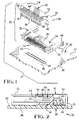
- FIGURE 1 is a perspective view of a shroud made in accordance with the invention exploded from a connector having surface mounted terminals, the connector being exploded from a circuit board to which the connector and shroud are to be mounted.
- FIGURE 2 is a cross-sectional view of the assembled shroud and connector.
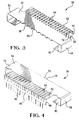
- FIGURE 3 is a perspective view of the front of the shroud of Figure 1.
- FIGURE 4 is a perspective view taken from the back of the shroud of Figure 1.
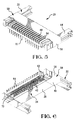
- FIGURE 5 is a view similar to Figure 4 with the shroud mounted on the connector of Figure 1.
- FIGURE 6 is a view of the assembly of Figure 5 taken from the board, mounting surface of the connector.
- FIGURE 7 shows the connector of Figure 5 mounted to one side of a circuit board and having a second shrouded surface mount connector exploded from the bottom of the circuit board for a stacked configuration.
- FIGURE 8 is a perspective view of the shroud used with the second or bottom board surface mounted connector.
- FIGURE 9 shows a stacked assembly of connectors having surface mounted leads and ground shrouds.
- FIGURE 10 is a cross-sectional view of the assembly of Figure 9.
- Electrical connector assembly 20 of the present invention includes electrical connector 22 and a shroud 50.
- connector 22 is shown as a top board surface mounted connector for a card reader. It is to be understood that the improved shroud of the present invention may also be used with receptacle connectors to be mated with shielded or unshielded plug connectors.
- the memory cards need to be oriented in a specific direction.
- the embodiment shown herein is for memory cards having the ground contacts on their upper surfaces.
- the assembly may also include an eject mechanism for the card proximate the circuit board.
- the connectors shown herein can be used in combination with numerous ejector mechanisms as known in the art.
- the connector 22 of the present invention includes a housing 24 having a first major or board remote side 26 and an opposed second major or board proximate side 28, and opposed minor sides 30 together defining a card receiving mouth 32.
- a portion of the card receiving mouth 32 defines a card receiving space 34.
- a plurality of electrical terminals 36 are disposed within the housing 24, the terminals 36 having first and second connecting portions 38,40 respectively.
- the first connecting portions 38 extend into the card receiving space 34 and are adapted for mating with complementary terminals of a memory card (not shown).
- the second connecting portions 40 include as contacts at leading ends 42 adapted for being surface mounted to respective circuit pads 84 of a circuit board 80, as best seen in Figure 1.
- connector 22 further includes card guide arms 44 extending outwardly thereof for receiving a card.
- the housing is preferably made from high temperature dielectric materials that can withstand soldering temperatures in the range of 230°C, such as liquid crystal polymers and other materials known in the art.
- Conductive shroud 50 is a unitary member including a top plate surface 52 having first portion 54 and a second portion 62.
- First portion 54 includes a plurality of spring fingers 56 extending from the leading edge 55 thereof. Spring fingers 56 are adapted to be received in card receiving mouth 32 as seen in Figure 2 and electrically engage ground contacts on the memory card inserted into the mouth 32. Fingers 56 are of the type disclosed in the previously discussed patents.
- Shroud 50 includes side walls 58 extending from the first portion 54.
- Shroud 50 further includes lower flanges 60 extending from the side walls 58 adapted to extend beneath the connector housing 24 as seen in Figure 6.
- Second portion 62 of shroud 50 further includes a back wall 66 having a plurality of terminal members 70 extending downwardly therefrom for electrical engagement with ground circuits in the circuit board. Terminal members 70 are held in true position by the strap-like section 68 of second shroud portion 62.
- terminal members 70 are shown as leads that are received in through-holes of a circuit board. It is to be understood that these leads may be surface mountable leads as well as the leads of the connector.
- the shroud is preferably made from a highly conductive material, such as phosphor-bronze or the like as known in the art.
- the second shroud portion 62 includes a plurality of apertures 64 or slots extending in the same direction as the terminal members 36.
- the slots 64 preferably extend rearwardly from the first plate portion 54 and partially down the back wall 66 of the shroud, ending at strap-like section 68.
- the slots 64 overly portions of the terminals 36 that extend outwardly of the housing 24 and are sufficient in number to permit visual inspection of the underlying connecting portions 40 and in particular contacts 42 when the shroud is disposed on the housing 24.
- top board surface mounted connector 20 In assembling top board surface mounted connector 20, plate portion 52 of shroud 50 is placed over the board remote surface 26 of housing 24, the spring fingers 56 are slid into position within the card receiving mouth 32 and side edges 58 and flange 60 are wrapped around the housing 24.
- the surface mounted leads In mounting connector 20 to top board surface 82, the surface mounted leads are brought into engagement with corresponding circuit pads 84 and terminal member leads 70 are inserted into the corresponding through-holes 86 as shown in Figure 2.
- the circuit pads 84 and through holes 86 are provided with solder paste or the like prior to mounting the connector and shroud assembly 20 to the board 80.
- the mounted assembly is then passed through an infrared oven at about 230°C using standard soldering procedures.
- the elongated apertures or slots 64 enable heat to reach the solder paste on the circuit pads causing it to melt thereby effecting electrical interconnection.
- solder paste is to be understood to include conductive adhesives and the like that may be used to effect mechanical and electrical interconnect between the leading ends 42 and pads 84.
- the slots 64 permit visual inspection of the soldered connections.
- Memory card assemblies are often used in stacked relationship.
- One method of stacking the connectors is by mounting memory cards on opposed surfaces 82, 88 of a circuit board 80 as shown in Figures 7-10.
- Figure 7 shows a connector assembly 20 as previously described mounted to a first or top major surface 82 of circuit board 80 and having a second connector assembly 120 exploded from the second or bottom major surface 88.
- the structure of the ground shrouded connector 120 differs from the ground shrouded structure of connector assembly 20 as previously described.
- the shroud 150 for assembly 120 is attached to the board proximate surface 28 of the connector housing 24, rather than the board remote surface 26 of the connector housing 24 as previously described.
- the shroud 150 has terminal members 170 extending upwardly from the main body portion 154, and requires no further structure to extend over the terminals.
- Shroud 150 includes a top plate surface 152 having side walls 158 and flanges 160.
- the leading edge 155 of plate section 152 includes spring fingers 156 which operate in the same manner as previously described.
- the terminal members 170 of shroud 150 are adapted to be received in the through-holes 92 of circuit board 80 as seen in Figures 1.
- Figures 9 and 10 show the assembled stacked card assembly with a respective terminal leads 42 secured to the circuit pads 84, 90 on the opposed surfaces 82, 88 of circuit board 80 and respective ground terminal members 70, 170 in their respective through holes 86, 92.
Landscapes
- Coupling Device And Connection With Printed Circuit (AREA)
- Details Of Connecting Devices For Male And Female Coupling (AREA)
- Shielding Devices Or Components To Electric Or Magnetic Fields (AREA)
- Multi-Conductor Connections (AREA)
Claims (3)
- Baugruppe aus Verbinder und Erdungsschutzkragen, die folgendes umfaßt: einen elektrischen Verbinder (22) mit einem Gehäuse (24) mit mehreren darin angeordneten Anschlüssen (36), wobei die Anschlüsse (36) sich aus dem Gehäuse (24) heraus erstreckende Kontaktabschnitte (42) zur elektrischen Ineingriffnahme von Schaltungen auf einer Leiterplatte (80) aufweisen; und einen zur elektrischen Ineingriffnahme von Erdungsschaltungen der Leiterplatte (80) ausgelegten Erdungsschutzkragen (50) zum Bilden eines Erdreferenz für die Anschlüsse (36), wobei der Schutzkragen (50) einen elektrisch leitfähigen plattenartigen Körper (52) mit einem ersten Teil (54), der an einer von der Platine entfernten Fläche (26) des Verbindergehäuses (24) angeordnet ist, und einem zweiten Teil (62), der sich über die Kontaktabschnitte (42) erstreckt und mit mindestens einem zweiten Kontaktabschnitt (70), der sich von dort aus zur Ineingriffnahme mit den Erdungsschaltungen der Leiterplatte (80) erstreckt, aufweist;
wobei die Baugruppe dadurch gekennzeichnet ist, daß die Kontaktabschnitte der Anschlüsse (36) oberflächenmontierbare Kontaktabschnitte (42) sind und der zweite Teil (62) des Schutzkragens (50) eine oder mehrere längliche Aperturen (64) aufweist, die sich in der Nähe der oberflächenmontierbaren Kontaktabschnitte (42) dort hindurch erstrecken, wodurch die Apertur(en) (64) bei Montage des Gehäuses (24) und des Schutzkragens (50) an der Leiterplatte (80) und Anlöten der oberflächenmontierbaren Kontaktabschnitte (42) an entsprechende Schaltungspads (84) auf der Platine es gestattet bzw. gestatten, daß ausreichende, beim Lötvorgang von einer von der Platine entfernten Quelle erzeugte wärme die Schaltungspads (84) erreicht und das Lot schmilzt, wodurch elektrische Ineingriffnahme der Anschlüsse (36) mit den Schaltungen auf der Platine (80) sichergestellt wird. - Baugruppe nach Anspruch 1, bei der der erste Schutzkragenteil mindestens einen Kontaktabschnitt (56) enthält, der ausgelegt ist, einen Erdungskontakt einer entsprechenden elektrischen Einrichtung in Eingriff zu nehmen.
- Baugruppe nach Anspruch 1 oder 2, bei dem der zweite Teil (62) des Schutzkragenkörpers (52) in einer Rückwand (66) mit Anschlußelementen (70) endet, die sich von dort aus zur elektrischen Ineingriffnahme mit Erdungsschaltungen erstrecken, wobei der zweite Teil mehrere der länglichen Aprturen (64) enthält, die sich von der oberen Fläche des zweiten Teils aus und teilweise die Rückwand hinunter erstrecken.
Applications Claiming Priority (2)
| Application Number | Priority Date | Filing Date | Title |
|---|---|---|---|
| US350202 | 1994-12-05 | ||
| US08/350,202 US5470259A (en) | 1994-12-05 | 1994-12-05 | Grounding shroud for surface mounted electrical connector |
Publications (2)
| Publication Number | Publication Date |
|---|---|
| EP0716480A1 EP0716480A1 (de) | 1996-06-12 |
| EP0716480B1 true EP0716480B1 (de) | 1999-02-03 |
Family
ID=23375654
Family Applications (1)
| Application Number | Title | Priority Date | Filing Date |
|---|---|---|---|
| EP95308215A Expired - Lifetime EP0716480B1 (de) | 1994-12-05 | 1995-11-16 | Erdungsumhüllung eines oberflächenmontierten Verbinders |
Country Status (7)
| Country | Link |
|---|---|
| US (1) | US5470259A (de) |
| EP (1) | EP0716480B1 (de) |
| JP (1) | JP3646894B2 (de) |
| KR (1) | KR100268571B1 (de) |
| CN (1) | CN1078395C (de) |
| DE (1) | DE69507679T2 (de) |
| MY (1) | MY131708A (de) |
Families Citing this family (50)
| Publication number | Priority date | Publication date | Assignee | Title |
|---|---|---|---|---|
| USRE40150E1 (en) | 1994-04-25 | 2008-03-11 | Matsushita Electric Industrial Co., Ltd. | Fiber optic module |
| US5717533A (en) | 1995-01-13 | 1998-02-10 | Methode Electronics Inc. | Removable optoelectronic module |
| US5546281A (en) | 1995-01-13 | 1996-08-13 | Methode Electronics, Inc. | Removable optoelectronic transceiver module with potting box |
| US6220878B1 (en) | 1995-10-04 | 2001-04-24 | Methode Electronics, Inc. | Optoelectronic module with grounding means |
| US5688130A (en) * | 1996-04-10 | 1997-11-18 | Molex Incorporated | Electrical connector assembly for pc cards |
| DE19621614C1 (de) * | 1996-05-30 | 1997-12-18 | Itt Cannon Gmbh | Steckverbinder |
| DE19624079C1 (de) * | 1996-06-17 | 1998-01-29 | Bosch Gmbh Robert | Kartenleser für Chipkarten |
| JP3066570B2 (ja) * | 1996-07-26 | 2000-07-17 | モレックス インコーポレーテッド | Pcカード用コネクタアッセンブリの製造方法 |
| US5697799A (en) * | 1996-07-31 | 1997-12-16 | The Whitaker Corporation | Board-mountable shielded electrical connector |
| US5725394A (en) * | 1996-10-11 | 1998-03-10 | Molex Incorporated | Grounding system for IC cards |
| JP3301924B2 (ja) * | 1996-10-17 | 2002-07-15 | アルプス電気株式会社 | Pcカード用コネクタ |
| JPH10255881A (ja) * | 1997-03-07 | 1998-09-25 | Molex Inc | 信号端子とグランド端子を備えた電気コネクタ |
| JP3299916B2 (ja) * | 1997-07-30 | 2002-07-08 | タイコエレクトロニクスアンプ株式会社 | 基板取付用コネクタ |
| US6085006A (en) | 1997-09-12 | 2000-07-04 | International Business Machines Corporation | Optical fiber link module with internal electromagnetic shield |
| EP0908978A3 (de) | 1997-10-09 | 2000-06-21 | Molex Incorporated | Kartensteckverbinderanordnung |
| EP0908977A3 (de) * | 1997-10-09 | 2000-06-21 | Molex Incorporated | Kartensteckverbinder mit verbessertem Schutzleiteranschluss |
| EP0908980A3 (de) * | 1997-10-09 | 2000-06-21 | Molex Incorporated | Kartensteckverbinder mit verbessertem Schutzleiteranschluss |
| US6039583A (en) * | 1998-03-18 | 2000-03-21 | The Whitaker Corporation | Configurable ground plane |
| US6203333B1 (en) | 1998-04-22 | 2001-03-20 | Stratos Lightwave, Inc. | High speed interface converter module |
| US6027365A (en) * | 1998-05-28 | 2000-02-22 | The Whitaker Corporation | Test card receptacle and header |
| JPH11345652A (ja) * | 1998-06-03 | 1999-12-14 | Amp Japan Ltd | カードコネクタ |
| US6068500A (en) * | 1998-07-28 | 2000-05-30 | Itt Manufacturing Enterprises, Inc. | Multi-contact PC card and host system |
| TW411043U (en) * | 1998-11-24 | 2000-11-01 | Hon Hai Prec Ind Co Ltd | Electric connector |
| US6965165B2 (en) * | 1998-12-21 | 2005-11-15 | Mou-Shiung Lin | Top layers of metal for high performance IC's |
| US7090509B1 (en) | 1999-06-11 | 2006-08-15 | Stratos International, Inc. | Multi-port pluggable transceiver (MPPT) with multiple LC duplex optical receptacles |
| JP2001035613A (ja) * | 1999-07-26 | 2001-02-09 | Fci Japan Kk | プリント基板用ソケット |
| US6220873B1 (en) | 1999-08-10 | 2001-04-24 | Stratos Lightwave, Inc. | Modified contact traces for interface converter |
| US6517382B2 (en) * | 1999-12-01 | 2003-02-11 | Tyco Electronics Corporation | Pluggable module and receptacle |
| US6227879B1 (en) * | 1999-12-21 | 2001-05-08 | Hon Hai Precision Ind. Co., Ltd. | Electrical connector with grounding shroud having board-locks for grasping a circuit board |
| TW464095U (en) * | 2000-12-26 | 2001-11-11 | Hon Hai Prec Ind Co Ltd | Connector for electric card |
| US6607308B2 (en) | 2001-02-12 | 2003-08-19 | E20 Communications, Inc. | Fiber-optic modules with shielded housing/covers having mixed finger types |
| US6659655B2 (en) | 2001-02-12 | 2003-12-09 | E20 Communications, Inc. | Fiber-optic modules with housing/shielding |
| JP4564201B2 (ja) * | 2001-05-02 | 2010-10-20 | 株式会社アイペックス | Icカード用コネクタ |
| TWM243880U (en) * | 2002-09-13 | 2004-09-11 | Quanta Comp Inc | Electrostatic discharge protection cover |
| US6685509B1 (en) | 2002-09-18 | 2004-02-03 | Hon Hai Precision Ind. Co., Ltd. | Shielded electronic card connector |
| JP2004146271A (ja) * | 2002-10-25 | 2004-05-20 | Fci Asia Technology Pte Ltd | 複数段式電気コネクタ |
| CN100514755C (zh) * | 2004-01-09 | 2009-07-15 | 莫列斯公司 | 电子卡连接器组合 |
| JP4152930B2 (ja) * | 2004-08-20 | 2008-09-17 | ヒロセ電機株式会社 | カード用コネクタ |
| US7442055B2 (en) * | 2006-07-18 | 2008-10-28 | Tyco Electronics Corporation | Straddle mount connector |
| KR100948130B1 (ko) * | 2007-02-27 | 2010-03-19 | 한국단자공업 주식회사 | 수직형 표면실장 커넥터 |
| JP4522440B2 (ja) * | 2007-07-26 | 2010-08-11 | 日本航空電子工業株式会社 | 基板搭載用コネクタ及びその相手方コネクタ並びにそれらを備えた電子機器 |
| US8000110B2 (en) * | 2008-03-24 | 2011-08-16 | Lsi Corporation | Connector hold down and method |
| US7661988B1 (en) * | 2008-11-17 | 2010-02-16 | Cheng Uei Precision Industry Co., Ltd. | Card connector |
| JP6152349B2 (ja) * | 2014-01-10 | 2017-06-21 | イリソ電子工業株式会社 | コネクタ用キャップ |
| CN103915728B (zh) * | 2014-04-01 | 2017-03-22 | 深圳市得润电子股份有限公司 | 一种带接地屏蔽的边缘卡连接器 |
| JP6508463B2 (ja) * | 2015-04-03 | 2019-05-08 | 第一精工株式会社 | コネクタ装置 |
| TWI535341B (zh) * | 2015-07-30 | 2016-05-21 | Giga Byte Tech Co Ltd | Reduce the structure of electromagnetic interference and reduce the electromagnetic interference method |
| US10389966B2 (en) * | 2016-09-02 | 2019-08-20 | Funai Electric Co., Ltd. | Display device |
| JP6211167B2 (ja) * | 2016-12-13 | 2017-10-11 | ホシデン株式会社 | 基板エッジコネクタ |
| CN111755916B (zh) * | 2019-03-28 | 2022-02-08 | 莫仕连接器(成都)有限公司 | 电连接器 |
Family Cites Families (20)
| Publication number | Priority date | Publication date | Assignee | Title |
|---|---|---|---|---|
| BE794849A (fr) * | 1972-02-08 | 1973-05-29 | Elco Corp | Plaque de circuit imprime |
| US3932016A (en) * | 1973-04-02 | 1976-01-13 | Stromberg-Carlson Corporation | Printed circuit card receptacle |
| US4046443A (en) * | 1976-05-27 | 1977-09-06 | Control Data Corporation | Printed circuit card guide |
| US4583807A (en) * | 1983-12-13 | 1986-04-22 | Amp Incorporated | Surface mount connector |
| US4756696A (en) * | 1985-12-06 | 1988-07-12 | Amp Incorporated | Solder joint inspection feature for surface mount connectors |
| US4732365A (en) * | 1987-01-23 | 1988-03-22 | Kloster Kenneth D | Bench mounted spring compressor |
| US4992052A (en) * | 1988-02-01 | 1991-02-12 | E. I. Du Pont De Nemours And Company | Modular connector system with high contact element density |
| JPH0541509Y2 (de) * | 1988-03-03 | 1993-10-20 | ||
| US4846727A (en) * | 1988-04-11 | 1989-07-11 | Amp Incorporated | Reference conductor for improving signal integrity in electrical connectors |
| US4941841A (en) * | 1988-06-09 | 1990-07-17 | Darden Julius C | Adapter and a removable slide-in cartridge for an information storage system |
| JPH0517826Y2 (de) * | 1988-07-29 | 1993-05-12 | ||
| US4861277A (en) * | 1988-11-21 | 1989-08-29 | American Telephone And Telegraph Company | Printed circuit card guide |
| GB2242317A (en) * | 1989-09-11 | 1991-09-25 | Itt Ind Ltd | Electrical connecting arrangement |
| GB9011506D0 (en) * | 1990-05-23 | 1990-07-11 | Bicc Plc | Optical fibre fusion splicing |
| US5035631A (en) * | 1990-06-01 | 1991-07-30 | Burndy Corporation | Ground shielded bi-level card edge connector |
| US5037330A (en) * | 1990-11-30 | 1991-08-06 | Amp Corporated | Stacked circular DIN connector |
| US5141445A (en) * | 1991-04-30 | 1992-08-25 | Thomas & Betts Corporation | Surface mounted electrical connector |
| DE69216288T2 (de) * | 1991-05-13 | 1997-04-24 | Fujitsu Ltd | Impedanz-angepasster elektrischer Steckverbinder |
| US5308251A (en) * | 1992-08-10 | 1994-05-03 | The Whitaker Corporation | Mounting bracket with ESD protection for an electrical connector |
| US5399105A (en) | 1994-04-29 | 1995-03-21 | The Whitaker Corporation | Conductive shroud for electrical connectors |
-
1994
- 1994-12-05 US US08/350,202 patent/US5470259A/en not_active Expired - Fee Related
-
1995
- 1995-11-16 EP EP95308215A patent/EP0716480B1/de not_active Expired - Lifetime
- 1995-11-16 DE DE69507679T patent/DE69507679T2/de not_active Expired - Fee Related
- 1995-12-01 KR KR1019950046010A patent/KR100268571B1/ko not_active Expired - Fee Related
- 1995-12-01 MY MYPI95003716A patent/MY131708A/en unknown
- 1995-12-04 CN CN95119065A patent/CN1078395C/zh not_active Expired - Fee Related
- 1995-12-05 JP JP34440595A patent/JP3646894B2/ja not_active Expired - Fee Related
Also Published As
| Publication number | Publication date |
|---|---|
| US5470259A (en) | 1995-11-28 |
| EP0716480A1 (de) | 1996-06-12 |
| KR960027067A (ko) | 1996-07-22 |
| DE69507679T2 (de) | 1999-07-22 |
| KR100268571B1 (ko) | 2000-10-16 |
| CN1078395C (zh) | 2002-01-23 |
| MY131708A (en) | 2007-08-30 |
| CN1131347A (zh) | 1996-09-18 |
| DE69507679D1 (de) | 1999-03-18 |
| JP3646894B2 (ja) | 2005-05-11 |
| JPH08255656A (ja) | 1996-10-01 |
Similar Documents
| Publication | Publication Date | Title |
|---|---|---|
| EP0716480B1 (de) | Erdungsumhüllung eines oberflächenmontierten Verbinders | |
| EP0772898B1 (de) | Verbesserte erdabdeckung für elektrische verbinder | |
| US5688130A (en) | Electrical connector assembly for pc cards | |
| US5496180A (en) | Surface mountable card edge connector | |
| JP3424683B2 (ja) | 電気コネクタ用導電シュラウド | |
| US5586893A (en) | IC card connector shield grounding | |
| US5046955A (en) | Active connector assembly | |
| US7077707B2 (en) | Modular jack connector having enhanced structure | |
| KR20020000001U (ko) | 향상된 접지 단자를 갖는 카드 커넥터 | |
| US5957705A (en) | Electrical connector including means for preventing relative dislocation of the conductive contacts and circuit board connectors | |
| US5112238A (en) | Electrical connector | |
| US20040087217A1 (en) | Electrical connector with rear retention mechanism of outer shell | |
| US6743047B2 (en) | Electrical connector with rear ground plate | |
| US4629267A (en) | Circuit terminating device | |
| US6322392B1 (en) | Ground plate structure for a PC card connector assembly | |
| EP0643448B1 (de) | Koaxialverbinder zur Verbindung mit Leiterplatten | |
| US5562499A (en) | Multiposition electrical connector filter adapter | |
| US5299942A (en) | Input-output electrical connector | |
| US4702706A (en) | Electrical connecting device including socket therefor | |
| US5967806A (en) | Electrical connector arrangement | |
| US4580857A (en) | Circuit terminating clip | |
| CA1216644A (en) | Electrical connecting device including socket therefor | |
| US4575165A (en) | Circuit to post interconnection device | |
| CA1259382A (en) | Backplane connector | |
| CA1247711A (en) | Circuit terminating device |
Legal Events
| Date | Code | Title | Description |
|---|---|---|---|
| PUAI | Public reference made under article 153(3) epc to a published international application that has entered the european phase |
Free format text: ORIGINAL CODE: 0009012 |
|
| AK | Designated contracting states |
Kind code of ref document: A1 Designated state(s): DE FR GB IE IT NL |
|
| 17P | Request for examination filed |
Effective date: 19961122 |
|
| 17Q | First examination report despatched |
Effective date: 19970211 |
|
| GRAG | Despatch of communication of intention to grant |
Free format text: ORIGINAL CODE: EPIDOS AGRA |
|
| GRAG | Despatch of communication of intention to grant |
Free format text: ORIGINAL CODE: EPIDOS AGRA |
|
| GRAH | Despatch of communication of intention to grant a patent |
Free format text: ORIGINAL CODE: EPIDOS IGRA |
|
| GRAH | Despatch of communication of intention to grant a patent |
Free format text: ORIGINAL CODE: EPIDOS IGRA |
|
| GRAA | (expected) grant |
Free format text: ORIGINAL CODE: 0009210 |
|
| AK | Designated contracting states |
Kind code of ref document: B1 Designated state(s): DE FR GB |
|
| REG | Reference to a national code |
Ref country code: IE Ref legal event code: FG4D |
|
| REF | Corresponds to: |
Ref document number: 69507679 Country of ref document: DE Date of ref document: 19990318 |
|
| ET | Fr: translation filed | ||
| RBV | Designated contracting states (corrected) |
Designated state(s): DE FR GB |
|
| NLV5 | Nl: annulment (art. 75) | ||
| PLBE | No opposition filed within time limit |
Free format text: ORIGINAL CODE: 0009261 |
|
| STAA | Information on the status of an ep patent application or granted ep patent |
Free format text: STATUS: NO OPPOSITION FILED WITHIN TIME LIMIT |
|
| 26N | No opposition filed | ||
| REG | Reference to a national code |
Ref country code: IE Ref legal event code: MM4A |
|
| REG | Reference to a national code |
Ref country code: GB Ref legal event code: IF02 |
|
| PGFP | Annual fee paid to national office [announced via postgrant information from national office to epo] |
Ref country code: GB Payment date: 20031002 Year of fee payment: 9 |
|
| PGFP | Annual fee paid to national office [announced via postgrant information from national office to epo] |
Ref country code: FR Payment date: 20031105 Year of fee payment: 9 |
|
| PGFP | Annual fee paid to national office [announced via postgrant information from national office to epo] |
Ref country code: DE Payment date: 20031128 Year of fee payment: 9 |
|
| PG25 | Lapsed in a contracting state [announced via postgrant information from national office to epo] |
Ref country code: GB Free format text: LAPSE BECAUSE OF NON-PAYMENT OF DUE FEES Effective date: 20041116 |
|
| PG25 | Lapsed in a contracting state [announced via postgrant information from national office to epo] |
Ref country code: DE Free format text: LAPSE BECAUSE OF NON-PAYMENT OF DUE FEES Effective date: 20050601 |
|
| GBPC | Gb: european patent ceased through non-payment of renewal fee |
Effective date: 20041116 |
|
| PG25 | Lapsed in a contracting state [announced via postgrant information from national office to epo] |
Ref country code: FR Free format text: LAPSE BECAUSE OF NON-PAYMENT OF DUE FEES Effective date: 20050729 |
|
| REG | Reference to a national code |
Ref country code: FR Ref legal event code: ST |