EP0718964A2 - Circuit oscillateur commutable et procédé - Google Patents
Circuit oscillateur commutable et procédé Download PDFInfo
- Publication number
- EP0718964A2 EP0718964A2 EP95120187A EP95120187A EP0718964A2 EP 0718964 A2 EP0718964 A2 EP 0718964A2 EP 95120187 A EP95120187 A EP 95120187A EP 95120187 A EP95120187 A EP 95120187A EP 0718964 A2 EP0718964 A2 EP 0718964A2
- Authority
- EP
- European Patent Office
- Prior art keywords
- fet
- oscillator
- source
- circuit
- drain
- Prior art date
- Legal status (The legal status is an assumption and is not a legal conclusion. Google has not performed a legal analysis and makes no representation as to the accuracy of the status listed.)
- Ceased
Links
- 238000000034 method Methods 0.000 title claims description 6
- 230000010355 oscillation Effects 0.000 claims description 28
- 239000003990 capacitor Substances 0.000 claims description 25
- 230000005540 biological transmission Effects 0.000 claims description 18
- 230000005669 field effect Effects 0.000 claims description 12
- JBRZTFJDHDCESZ-UHFFFAOYSA-N AsGa Chemical compound [As]#[Ga] JBRZTFJDHDCESZ-UHFFFAOYSA-N 0.000 claims description 11
- 229910001218 Gallium arsenide Inorganic materials 0.000 claims description 11
- 238000005513 bias potential Methods 0.000 claims 2
- 101100484930 Saccharomyces cerevisiae (strain ATCC 204508 / S288c) VPS41 gene Proteins 0.000 description 10
- 238000012545 processing Methods 0.000 description 4
- 230000003321 amplification Effects 0.000 description 3
- 238000005516 engineering process Methods 0.000 description 3
- 238000003199 nucleic acid amplification method Methods 0.000 description 3
- 238000013459 approach Methods 0.000 description 2
- 238000013461 design Methods 0.000 description 2
- 238000010586 diagram Methods 0.000 description 2
- 238000004519 manufacturing process Methods 0.000 description 2
- 230000006978 adaptation Effects 0.000 description 1
- 230000003466 anti-cipated effect Effects 0.000 description 1
- 230000000295 complement effect Effects 0.000 description 1
- 238000012986 modification Methods 0.000 description 1
- 230000004048 modification Effects 0.000 description 1
- 239000004065 semiconductor Substances 0.000 description 1
- 238000001228 spectrum Methods 0.000 description 1
Images

Classifications
-
- H—ELECTRICITY
- H03—ELECTRONIC CIRCUITRY
- H03B—GENERATION OF OSCILLATIONS, DIRECTLY OR BY FREQUENCY-CHANGING, BY CIRCUITS EMPLOYING ACTIVE ELEMENTS WHICH OPERATE IN A NON-SWITCHING MANNER; GENERATION OF NOISE BY SUCH CIRCUITS
- H03B5/00—Generation of oscillations using amplifier with regenerative feedback from output to input
- H03B5/18—Generation of oscillations using amplifier with regenerative feedback from output to input with frequency-determining element comprising distributed inductance and capacitance
- H03B5/1864—Generation of oscillations using amplifier with regenerative feedback from output to input with frequency-determining element comprising distributed inductance and capacitance the frequency-determining element being a dielectric resonator
- H03B5/187—Generation of oscillations using amplifier with regenerative feedback from output to input with frequency-determining element comprising distributed inductance and capacitance the frequency-determining element being a dielectric resonator the active element in the amplifier being a semiconductor device
- H03B5/1876—Generation of oscillations using amplifier with regenerative feedback from output to input with frequency-determining element comprising distributed inductance and capacitance the frequency-determining element being a dielectric resonator the active element in the amplifier being a semiconductor device the semiconductor device being a field-effect device
-
- H—ELECTRICITY
- H03—ELECTRONIC CIRCUITRY
- H03D—DEMODULATION OR TRANSFERENCE OF MODULATION FROM ONE CARRIER TO ANOTHER
- H03D7/00—Transference of modulation from one carrier to another, e.g. frequency-changing
- H03D7/16—Multiple-frequency-changing
- H03D7/161—Multiple-frequency-changing all the frequency changers being connected in cascade
-
- H—ELECTRICITY
- H03—ELECTRONIC CIRCUITRY
- H03J—TUNING RESONANT CIRCUITS; SELECTING RESONANT CIRCUITS
- H03J5/00—Discontinuous tuning; Selecting predetermined frequencies; Selecting frequency bands with or without continuous tuning in one or more of the bands, e.g. push-button tuning, turret tuner
- H03J5/24—Discontinuous tuning; Selecting predetermined frequencies; Selecting frequency bands with or without continuous tuning in one or more of the bands, e.g. push-button tuning, turret tuner with a number of separate pretuned tuning circuits or separate tuning elements selectively brought into circuit, e.g. for waveband selection or for television channel selection
- H03J5/242—Discontinuous tuning; Selecting predetermined frequencies; Selecting frequency bands with or without continuous tuning in one or more of the bands, e.g. push-button tuning, turret tuner with a number of separate pretuned tuning circuits or separate tuning elements selectively brought into circuit, e.g. for waveband selection or for television channel selection used exclusively for band selection
- H03J5/244—Discontinuous tuning; Selecting predetermined frequencies; Selecting frequency bands with or without continuous tuning in one or more of the bands, e.g. push-button tuning, turret tuner with a number of separate pretuned tuning circuits or separate tuning elements selectively brought into circuit, e.g. for waveband selection or for television channel selection used exclusively for band selection using electronic means
-
- H—ELECTRICITY
- H03—ELECTRONIC CIRCUITRY
- H03B—GENERATION OF OSCILLATIONS, DIRECTLY OR BY FREQUENCY-CHANGING, BY CIRCUITS EMPLOYING ACTIVE ELEMENTS WHICH OPERATE IN A NON-SWITCHING MANNER; GENERATION OF NOISE BY SUCH CIRCUITS
- H03B2200/00—Indexing scheme relating to details of oscillators covered by H03B
- H03B2200/003—Circuit elements of oscillators
- H03B2200/0034—Circuit elements of oscillators including a buffer amplifier
-
- H—ELECTRICITY
- H03—ELECTRONIC CIRCUITRY
- H03B—GENERATION OF OSCILLATIONS, DIRECTLY OR BY FREQUENCY-CHANGING, BY CIRCUITS EMPLOYING ACTIVE ELEMENTS WHICH OPERATE IN A NON-SWITCHING MANNER; GENERATION OF NOISE BY SUCH CIRCUITS
- H03B2200/00—Indexing scheme relating to details of oscillators covered by H03B
- H03B2200/003—Circuit elements of oscillators
- H03B2200/0048—Circuit elements of oscillators including measures to switch the frequency band, e.g. by harmonic selection
-
- H—ELECTRICITY
- H03—ELECTRONIC CIRCUITRY
- H03B—GENERATION OF OSCILLATIONS, DIRECTLY OR BY FREQUENCY-CHANGING, BY CIRCUITS EMPLOYING ACTIVE ELEMENTS WHICH OPERATE IN A NON-SWITCHING MANNER; GENERATION OF NOISE BY SUCH CIRCUITS
- H03B2200/00—Indexing scheme relating to details of oscillators covered by H03B
- H03B2200/006—Functional aspects of oscillators
- H03B2200/0062—Bias and operating point
-
- H—ELECTRICITY
- H03—ELECTRONIC CIRCUITRY
- H03B—GENERATION OF OSCILLATIONS, DIRECTLY OR BY FREQUENCY-CHANGING, BY CIRCUITS EMPLOYING ACTIVE ELEMENTS WHICH OPERATE IN A NON-SWITCHING MANNER; GENERATION OF NOISE BY SUCH CIRCUITS
- H03B5/00—Generation of oscillations using amplifier with regenerative feedback from output to input
- H03B5/18—Generation of oscillations using amplifier with regenerative feedback from output to input with frequency-determining element comprising distributed inductance and capacitance
- H03B5/1841—Generation of oscillations using amplifier with regenerative feedback from output to input with frequency-determining element comprising distributed inductance and capacitance the frequency-determining element being a strip line resonator
- H03B5/1847—Generation of oscillations using amplifier with regenerative feedback from output to input with frequency-determining element comprising distributed inductance and capacitance the frequency-determining element being a strip line resonator the active element in the amplifier being a semiconductor device
- H03B5/1852—Generation of oscillations using amplifier with regenerative feedback from output to input with frequency-determining element comprising distributed inductance and capacitance the frequency-determining element being a strip line resonator the active element in the amplifier being a semiconductor device the semiconductor device being a field-effect device
Definitions
- This invention relates to switchable oscillator circuits and to a method of switching between different oscillator frequencies by using such circuits. More particularly, but not exclusively, the invention relates to fixed-frequency oscillators used in Gallium Arsenide Monolithic Microwave Integrated Circuit (MMIC) downconverters for Low Noise Block Downconverters of Direct Broadcast Satellite (DBS) television systems.
- MMIC Gallium Arsenide Monolithic Microwave Integrated Circuit
- DBS Direct Broadcast Satellite
- Direct Broadcast Satellite television transmission receivers comprise a Low Noise Block Downconverter (LNB) mounted on an antenna or satellite dish connected, via coaxial cable, to an indoor tuner attached to a television set or VCR.
- LNB Low Noise Block Downconverter
- the LNB is connected to the antenna or dish and converts the satellite signal received by the antenna to a frequency and signal level suitable for processing by the tuner and television or VCR electronics.
- the Low Noise Block Downconverter assembly typically includes a monolithic microwave integrated circuit (MMIC) downconverter mounted on a printed circuit board along with support circuitry, additional amplifier stages and filters to provide increased amplification and reduced front end noise.
- MMIC monolithic microwave integrated circuit
- the LNB Downconverter receives radio frequencies of approximately 11 GHz to 12 GHz and first amplifies the signals through several high electron mobility transistors (HEMTs) and two amplifier stages in the MMIC.
- the MMIC also downconverts the RF signals to an intermediate frequency (IF) of approximately 1000 MHz in a mixer, then amplifies the IF signal.
- the mixer operates by combining the received radio frequency (RF) signals with an internal frequency reference produced by a local oscillator (LO) as is known in the art.
- the IF signals are the difference between the RF and LO frequency signals.
- a new Direct Broadcast Satellite system operates over a broad RF range of 10.7 GHz to 12.75 GHz.
- Using one local oscillator frequency in the mixer would produce IF signals that are too broad and high in frequency to utilize existing converter box and coaxial cable technology.
- a solution is to use two separate local oscillator frequencies.
- the present invention provides a technique to implement a two frequency local oscillator with good switching characteristics and at a low cost.
- the oscillator circuit switches between two different frequencies without requiring conventional switches.
- the RF band of the DBS system is separated into two bands such that when each RF band is mixed with the appropriate oscillator frequency, an IF bandwidth capable of being processed by currently available hardware is produced.
- the switched oscillator consists of two FET oscillators with a common output. It is controlled by a voltage applied at the gate of each FET. When the gate voltage is zero volts, the FET oscillator oscillates at a frequency determined by a dielectric resonator. When the gate voltage is sufficiently negative, the FET oscillator is "pinched-off" and little or no current flows through the device. At pinch-off, oscillation cannot occur. By applying zero volts to the gate of one FET and a negative voltage (at pinch-off) to the gate of the second FET, the switched oscillator provides two oscillation frequencies. Another advantage of the switched oscillator is that the device does not draw any bias current at pinch-off which conserves DC power. Additionally, the output impedance of the FET is extremely high at pinch-off or effectively an open circuit. Therefore, the pinched-off oscillator does not load, attenuate or interfere with the output signal of the adjacent operational oscillator.
- the circuit can be implemented in a GaAs MMIC downconverter with supporting circuitry in an LNB.
- This implementation allows existing converter box and coaxial cable designs to be utilized with the new DBS system.
- the MMIC comprises a mixer circuit that combines one local oscillator signal with one radio frequency band and the second local oscillator signal with another radio frequency band to produce sum and difference frequency signals.
- An intermediate frequency signal (the difference signal) is selected by a low pass filter coupled to the mixer circuit.
- An amplifier circuit amplifies the intermediate frequency signal from the low pass filter for an output signal of the MMIC.
- a switchable oscillator circuit for generating microwave energy at a selected one of a plurality of microwave frequencies, comprising: a plurality of field effect transistor (FET) oscillators, operable for oscillation at different microwave frequencies, each FET oscillator comprising an input and output, and the outputs of the FET oscillators being connected together; a bias supply connected to the outputs of the FET oscillators; first and second inputs, each for receiving either a first or second potential; and wherein the FET oscillators each comprise a FET responsive to a first potential for enabling the corresponding FET oscillator to oscillate and responsive to a second potential for disabling or pinching-off the corresponding FET oscillator.
- FET field effect transistor
- a method of switching between oscillator frequencies of at least first and second field effect transistor (FET) oscillators comprising the steps of: connecting the outputs of each oscillator together to a common output; applying a first potential to the input of the first FET oscillator to cause oscillation thereof while applying a second potential to the input of the second FET oscillator to cause pinch-off thereof, thereby generating a first oscillation frequency at the common output; and the applying a first potential to the input of the first FET oscillator to cause pinch-off thereof, while applying a second potential to the input of the second FET oscillator to cause oscillation thereof, thereby generating a second oscillation frequency at the common output.
- FET field effect transistor
- the present invention also embraces a monolithic microwave integrated circuit (MMIC) downconverter for providing lower frequency output signals derived from radio frequency input signals, comprising: a mixer circuit for producing sum and difference frequency signals from an oscillator signal and a radio frequency signal from the input signals; a low pass filter connected to the mixer circuit for selecting an intermediate frequency signal from one of the sum and difference frequency signals; an amplifier circuit connected to the low pass filter for amplifying the intermediate frequency signal for the output signals; and a switchable oscillator frequency signal circuit for providing either a first or a second oscillator signal, as the oscillator signal to the mixer circuit.
- MMIC monolithic microwave integrated circuit
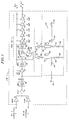
- FIG. 1 illustrates a block diagram of a Low Noise Block Downconverter, LNB 1, for use in the new Direct Broadcast Satellite (DBS) receiver system.
- the radio frequency (RF) input is received by an antenna or dish (not shown) from a satellite transmission.
- the RF input may be horizontally polarized, RF IN (Horizontal) 2, or vertically polarized, RF IN (Vertical) 4, depending on the broadcast channel to which the television is tuned.
- the LNB Downconverter 1 is mounted on the antenna. It converts the received RF signal frequency to an intermediate frequency and amplifies the signal for processing by receiver electronics (not shown) inside, for example, the home.
- the RF IN (Horizontal) 2 or RF IN (Vertical) 4 are within the frequency band 10.7 GHz to 12.75 GHz and are received by high electron mobility transistors (HEMTs), HEMT 10 and HEMT 12 respectively, for amplification of the signal.
- the HEMTs provide high frequency, low noise amplification of the RF signals.
- the amplified RF IN (Horizontal) 2 or RF IN (Vertical) 4 signal is further amplified by HEMT 14.
- the amplified RF signal is filtered by the BPF 16, an image-reject band pass filter, to remove unwanted signals from other sources or noise produced by the HEMTs outside of the RF signal frequency band.
- the output, RF IN 24, is input to the MMIC 22 for downconversion to an intermediate frequency (IF) signal, IF OUT 8, for processing by the receiver electronics.
- IF intermediate frequency
- the MMIC 22 receives the RF IN 24 and amplifies the signal in the RF AMP 26.
- the amplified RF signal is filtered in the BPF 28, an image-reject band pass filter, to reduce noise produced by the RF AMP 26 in the image band.
- the filtered and amplified RF signal, RF 30, is input to the mixer 32 where it is combined with local oscillator signal, LO 34, to produce sum and difference frequency signals of the RF 30 and LO 34 signals.
- the LPF 62 a low pass filter, selects an intermediate frequency signal, which is the difference signal, and provides it to IF amplifier, IF AMP 64.
- the amplified intermediate frequency signal is further amplified in four additional amplifier stages within the MMIC 22 comprising IF AMP 66, IF AMP 68, IF AMP 70, and IF AMP 72.
- the amplified signal, IF OUT 8 is then output to a converter box, or television or VCR receiver electronics for processing.
- FIG. 2 illustrates portion 23 of the MMIC 22 and is referenced in the following discussion.
- the mixer 32 combines the RF signal 30 with the amplified LO signal 34.
- the local oscillator (LO) signal 38 is one of two frequencies, 9.75 GHz or 10.6 GHz, and is connected to the input of the LO amplifier, LO AMP 36, which produces an amplified local oscillator (LO) signal 34.
- LO local oscillator
- a spectrum of frequencies from the sum and difference of the RF signal 30 and LO signal 34 and harmonics are generated at the output of the mixer 32.
- the low pass filter, LPF 62 attenuates all but the difference frequencies to provide an intermediate frequency (IF) signal 60.
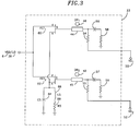
- the LO signal 34 is generated by a switchable oscillator circuit 23 and amplified by the LO amplifier, LO AMP 36.
- the switchable oscillator circuit 23 is comprised of local oscillators 40 and 42, internal to the MMIC 22, and transmission lines 44 and 45 connected to the respective local oscillators, dielectric resonators 46 and 48 coupled to the respective transmission lines, bias resistors 54 and 55 connected in parallel with bypass capacitors 56 and 57 and termination resistors 58 and 59 and to the other end of the transmission lines.
- the termination resistors 58 and 59 are 50 ohms and prevent unwanted oscillations at undesirable frequencies.
- Inputs for receiving a voltage VG1 50 or VG2 52 are connected to the respective bias resistors 54 and 55.
- the local oscillators 40 and 42 are comprised of a FET (FET1 80 or FET2 82) in a common source configuration with source inductors, LS 86 and LS 87, in series with source bias resistors, RS 88 and RS 89, and both connected in parallel with source capacitors, CS 84 and CS 85, and connected to the source, s, of the FET.
- the FET1 80 and FET2 82 are self-biased in a conventional manner with the gate to source voltage at the source, s, determined by the drain current through the source bias resistors, RS 88 and RS 89.
- the reactive feedback circuitry comprised of the source capacitors, CS 84 and CS 85, in conjunction with the source inductors, LS 86 and LS 87, and source resistors, RS 88 and RS 89, creates a negative resistance within the device allowing FET1 80 and FET2 82 to oscillate.
- the gate, g, of FET1 80 and FET2 82 is connected to the transmission lines 44 and 45, respectively, to which the dielectric resonators 46 and 48 are respectively coupled for providing a stable oscillation frequency.
- the drains, d, of FET1 80 and FET2 82 are connected together at 39 and to the LO amplifier, LO AMP 36, as well as the bias supply, VDD 6.
- the switchable oscillator 23 provides one of two local oscillator frequencies, 9.75 GHz from oscillator LO 40 or 10.6 GHz from oscillator LO 42, for mixing with the RF signal 30 as described above. Switching between the two oscillator frequencies is achieved with pinch-off control of the oscillator FETs, 80 and 82.
- oscillator LO 40 The concept of pinch-off control of a single oscillator, LO 40, is illustrated with the following example. The following is a description of oscillator LO 40. It will be understood that oscillator LO 42 operates in the same manner as oscillator LO 40 and the description will not be repeated. With a voltage VG1 50 equal to zero volts applied to the gate input, g, of the FET1 80 through resistor 54, the FET oscillator, LO 40, will oscillate at the frequency of the dielectric resonator DR1 46 while the bias voltage, VDD 6, is applied.
- VDD 6 bias voltage
- the current flow within the device, FET1 80, from the drain, d, to the source, s, is reduced to essentially zero.
- the negative voltage sufficient to cause this condition is called the pinch-off voltage, Vp.
- the LO 40 is not oscillating, removing the possibility of electrical interference, and bias current is not being drawn, conserving DC power.
- the output impedance of FET1 80 is extremely high at pinch-off such that it is effectively an open circuit. Therefore, at pinch-off, LO 40 will not load, attenuate or interfere with the output signal of the adjacent oscillating LO 42.
- One of the oscillator frequencies is obtained by applying VG1 equal to zero volts to the gate, g, of FET1 80 while applying VG2 equal to Vp volts to the gate, g, of FET2 82.
- the other oscillator frequency is obtained by applying VG1 equal to Vp volts to the gate, g, of FET1 80 while applying VG2 equal to zero volts to the gate, g, of FET2 82.
- the voltages VG1 50 and VG2 52 are controlled by circuitry within the LNB 1 (not shown) that receives a control signal through a coaxial cable from the set top converter or indoor tuner and applies the appropriate voltage levels to the inputs of the FET oscillators to switch to the proper oscillator frequency depending on the channel that is selected.
- FIG. 3 provides the same function as the circuit depicted in FIG. 2 with fewer components, since the source capacitor, CS 84, source inductor, LS 86 and source bias resistor, RS 88, are common to FET1 80 and FET2 82. As shown in FIG. 3, the source inductor, LS 86 is connected in series with the source bias resistor, RS 88 and both are connected in parallel with the source capacitor, CS 84 and connected to the sources, s, of both FET1 80 and FET2 82. The remaining circuitry is connected in the same manner as that of the embodiment described for FIG. 2.
- n-channel depletion mode FET could be utilized within the switchable oscillator circuit in place of the depletion mode devices FET1 80 and FET2 82.
- the source bias resistors RS 88 and RS 89 of the embodiment of FIG. 2 or RS 88 of the embodiment of FIG. 3 are not required for self-biasing of the enhancement mode FET.
- a negative voltage source is not required as the threshold voltage (analogous to the pinch-off voltage of the depletion mode device) i.e., the voltage at which the drain, d, to source, s, current is essentially zero, is approximately zero volts.
- a positive voltage applied to the gate, g, of the enhancement mode FET turns on the device allowing conduction of drain current through the FET.
- the MMIC 22 of FIG. 1 is fabricated from Gallium Arsenide, GaAs, and assembled into a single package with input terminals for the radio frequency signal RF IN 24, the bias supply VDD 6, and the inputs to the local oscillators LO 40 and LO 42, an output terminal for the intermediate frequency output signal IF OUT 8, and three ground terminals (not shown, but depicted by ground symbols).
- the ground symbols are representative of a reference potential.
- the bias supply input terminal is connected to the active load and amplifier circuit IF AMP 64, the RF AMP 26, the local oscillators LO 40 and LO 42, and the IF signal amplifiers IF AMP 66, IF AMP 68, IF AMP 70, and IF AMP 72 for supplying the DC bias voltage.
- n-channel FET has been described in the embodiments of FIG. 2 and FIG. 3; however, a complementary p-channel FET could be utilized instead of the n-channel device.
- the p-channel FET operation is the same as that of the n-channel device except that pinch-off results from a sufficiently positive voltage applied to the gate input and the currents are reversed.
- the above-described embodiments employ two oscillation frequencies; however, additional frequencies can be obtained by connecting additional local oscillators at 39 and providing supporting circuitry and a gate bias voltage for each within the LNB 1 (in this case, if desired, the potential for causing oscillation can be successively applied to a different one of the FET oscillators whilst applying a potential to cause pinch-off to the inputs of the remaining FET oscillators).
Landscapes
- Engineering & Computer Science (AREA)
- Power Engineering (AREA)
- Inductance-Capacitance Distribution Constants And Capacitance-Resistance Oscillators (AREA)
Applications Claiming Priority (2)
| Application Number | Priority Date | Filing Date | Title |
|---|---|---|---|
| US35952394A | 1994-12-20 | 1994-12-20 | |
| US359523 | 1994-12-20 |
Publications (2)
| Publication Number | Publication Date |
|---|---|
| EP0718964A2 true EP0718964A2 (fr) | 1996-06-26 |
| EP0718964A3 EP0718964A3 (fr) | 1996-10-02 |
Family
ID=23414188
Family Applications (1)
| Application Number | Title | Priority Date | Filing Date |
|---|---|---|---|
| EP95120187A Ceased EP0718964A3 (fr) | 1994-12-20 | 1995-12-20 | Circuit oscillateur commutable et procédé |
Country Status (1)
| Country | Link |
|---|---|
| EP (1) | EP0718964A3 (fr) |
Cited By (4)
| Publication number | Priority date | Publication date | Assignee | Title |
|---|---|---|---|---|
| WO1998017010A3 (fr) * | 1996-10-11 | 1998-06-04 | Ericsson Telefon Ab L M | Recepteur multibande |
| EP0845855A3 (fr) * | 1996-11-27 | 1998-07-01 | TDK Corporation | Oscillateur commandé en tension |
| EP1408579A1 (fr) * | 2002-10-09 | 2004-04-14 | Sharp Kabushiki Kaisha | Bloc convertisseur abaisseur à faible bruit comprenant plusieurs oscillateurs |
| CN104682875A (zh) * | 2013-11-27 | 2015-06-03 | 中国航空工业集团公司雷华电子技术研究所 | 一种有效抑制杂散的宽带信号产生方法 |
Family Cites Families (4)
| Publication number | Priority date | Publication date | Assignee | Title |
|---|---|---|---|---|
| US4485355A (en) * | 1982-02-02 | 1984-11-27 | Texas Instruments Incorporated | Switched geometry oscillator |
| JPS60149227A (ja) * | 1984-01-13 | 1985-08-06 | Sony Corp | Shf受信機 |
| CA1329640C (fr) * | 1987-07-24 | 1994-05-17 | Miyoshi Yamauchi | Convertisseur a faible bruit exterieur pour la reception d'emissions diffusees par satellite |
| KR910003234B1 (ko) * | 1988-05-18 | 1991-05-24 | 삼성전자 주식회사 | 위성방송 수신용 저잡음 블럭 변환기 |
-
1995
- 1995-12-20 EP EP95120187A patent/EP0718964A3/fr not_active Ceased
Cited By (7)
| Publication number | Priority date | Publication date | Assignee | Title |
|---|---|---|---|---|
| WO1998017010A3 (fr) * | 1996-10-11 | 1998-06-04 | Ericsson Telefon Ab L M | Recepteur multibande |
| US5995815A (en) * | 1996-10-11 | 1999-11-30 | Telefonaktiebolaget Lm Ericsson | Multiple band receiver |
| EP0845855A3 (fr) * | 1996-11-27 | 1998-07-01 | TDK Corporation | Oscillateur commandé en tension |
| US5982240A (en) * | 1996-11-27 | 1999-11-09 | Tdk Corporation | Voltage controlled oscillator using a plurality of switchable oscillators |
| EP1408579A1 (fr) * | 2002-10-09 | 2004-04-14 | Sharp Kabushiki Kaisha | Bloc convertisseur abaisseur à faible bruit comprenant plusieurs oscillateurs |
| US7177618B2 (en) | 2002-10-09 | 2007-02-13 | Sharp Kabushiki Kaisha | Low noise block down converter with a plurality of local oscillators |
| CN104682875A (zh) * | 2013-11-27 | 2015-06-03 | 中国航空工业集团公司雷华电子技术研究所 | 一种有效抑制杂散的宽带信号产生方法 |
Also Published As
| Publication number | Publication date |
|---|---|
| EP0718964A3 (fr) | 1996-10-02 |
Similar Documents
| Publication | Publication Date | Title |
|---|---|---|
| KR100196241B1 (ko) | 마이크로파 혼합 회로 | |
| US7103331B2 (en) | Low noise block down converter with reduced power consumption | |
| US5940750A (en) | Low-cost low noise block down-converter with a self-oscillating mixer for satellite broadcast receivers | |
| KR100352658B1 (ko) | 트랜시버집적회로패키지 | |
| US5551076A (en) | Circuit and method of series biasing a single-ended mixer | |
| EP1187310A2 (fr) | Mélangeur utilisant une cellule à Gilbert | |
| US4464636A (en) | Wideband IF amplifier with complementary GaAs FET-bipolar transistor combination | |
| US5649312A (en) | MMIC downconverter for a direct broadcast satellite low noise block downconverter | |
| US7130577B2 (en) | Low noise converter employed in satellite broadcast reception system and receiver apparatus | |
| JP2558258B2 (ja) | マイクロ波受信機 | |
| JP3036717B2 (ja) | コンバータ回路 | |
| US6861891B2 (en) | Sub-harmonic mixer | |
| US6400224B2 (en) | Two stage low noise amplifier | |
| EP0718964A2 (fr) | Circuit oscillateur commutable et procédé | |
| US5748049A (en) | Multi-frequency local oscillators | |
| CN1118188C (zh) | 用于接收卫星广播的卫星直播调谐器 | |
| JP2608430B2 (ja) | 同調可能な発振器 | |
| Wang et al. | A low cost DBS low noise block downconverter with a DR stabilized MESFET self-oscillating mixer | |
| US6671505B1 (en) | Frequency converter | |
| US20020186326A1 (en) | Television tuner having simplified wiring for interconnection and having miniaturized integrated circuit | |
| US6157269A (en) | Local oscillator noise rejection circuit | |
| JPH05344018A (ja) | 受信マイクロ波信号のダウンコンバータ装置 | |
| JP2659573B2 (ja) | Ic化受信機 | |
| JP2578854B2 (ja) | 受信回路 | |
| EP0915530B1 (fr) | Circuit de sélection de polarisation |
Legal Events
| Date | Code | Title | Description |
|---|---|---|---|
| PUAI | Public reference made under article 153(3) epc to a published international application that has entered the european phase |
Free format text: ORIGINAL CODE: 0009012 |
|
| AK | Designated contracting states |
Kind code of ref document: A2 Designated state(s): DE FR GB IT |
|
| PUAL | Search report despatched |
Free format text: ORIGINAL CODE: 0009013 |
|
| AK | Designated contracting states |
Kind code of ref document: A3 Designated state(s): DE FR GB IT |
|
| 17P | Request for examination filed |
Effective date: 19970327 |
|
| 17Q | First examination report despatched |
Effective date: 19990210 |
|
| GRAG | Despatch of communication of intention to grant |
Free format text: ORIGINAL CODE: EPIDOS AGRA |
|
| STAA | Information on the status of an ep patent application or granted ep patent |
Free format text: STATUS: THE APPLICATION HAS BEEN REFUSED |
|
| 18R | Application refused |
Effective date: 20010628 |