EP0720174A2 - Dispositif de mémoire à semi-conducteurs à multi-états - Google Patents
Dispositif de mémoire à semi-conducteurs à multi-états Download PDFInfo
- Publication number
- EP0720174A2 EP0720174A2 EP95120254A EP95120254A EP0720174A2 EP 0720174 A2 EP0720174 A2 EP 0720174A2 EP 95120254 A EP95120254 A EP 95120254A EP 95120254 A EP95120254 A EP 95120254A EP 0720174 A2 EP0720174 A2 EP 0720174A2
- Authority
- EP
- European Patent Office
- Prior art keywords
- potential
- bit
- read
- generating
- sense amplifier
- Prior art date
- Legal status (The legal status is an assumption and is not a legal conclusion. Google has not performed a legal analysis and makes no representation as to the accuracy of the status listed.)
- Granted
Links
- 239000004065 semiconductor Substances 0.000 title claims description 10
- 230000003213 activating effect Effects 0.000 claims abstract description 36
- 239000003990 capacitor Substances 0.000 claims description 61
- 230000003139 buffering effect Effects 0.000 claims description 4
- 230000007704 transition Effects 0.000 description 13
- 238000010586 diagram Methods 0.000 description 12
- 238000005516 engineering process Methods 0.000 description 3
- 230000004048 modification Effects 0.000 description 3
- 238000012986 modification Methods 0.000 description 3
- 238000004904 shortening Methods 0.000 description 3
- 230000004936 stimulating effect Effects 0.000 description 3
- 101150005874 DEF1 gene Proteins 0.000 description 2
- 230000008859 change Effects 0.000 description 2
- 230000002093 peripheral effect Effects 0.000 description 2
- 101000873780 Homo sapiens m7GpppN-mRNA hydrolase Proteins 0.000 description 1
- 238000009792 diffusion process Methods 0.000 description 1
- 230000010354 integration Effects 0.000 description 1
- 102100035860 m7GpppN-mRNA hydrolase Human genes 0.000 description 1
- 239000000203 mixture Substances 0.000 description 1
- 230000009467 reduction Effects 0.000 description 1
- 230000009466 transformation Effects 0.000 description 1
Images


Classifications
-
- G—PHYSICS
- G11—INFORMATION STORAGE
- G11C—STATIC STORES
- G11C11/00—Digital stores characterised by the use of particular electric or magnetic storage elements; Storage elements therefor
- G11C11/21—Digital stores characterised by the use of particular electric or magnetic storage elements; Storage elements therefor using electric elements
- G11C11/34—Digital stores characterised by the use of particular electric or magnetic storage elements; Storage elements therefor using electric elements using semiconductor devices
- G11C11/40—Digital stores characterised by the use of particular electric or magnetic storage elements; Storage elements therefor using electric elements using semiconductor devices using transistors
- G11C11/401—Digital stores characterised by the use of particular electric or magnetic storage elements; Storage elements therefor using electric elements using semiconductor devices using transistors forming cells needing refreshing or charge regeneration, i.e. dynamic cells
- G11C11/4063—Auxiliary circuits, e.g. for addressing, decoding, driving, writing, sensing or timing
- G11C11/407—Auxiliary circuits, e.g. for addressing, decoding, driving, writing, sensing or timing for memory cells of the field-effect type
-
- G—PHYSICS
- G11—INFORMATION STORAGE
- G11C—STATIC STORES
- G11C11/00—Digital stores characterised by the use of particular electric or magnetic storage elements; Storage elements therefor
- G11C11/56—Digital stores characterised by the use of particular electric or magnetic storage elements; Storage elements therefor using storage elements with more than two stable states represented by steps, e.g. of voltage, current, phase, frequency
- G11C11/565—Digital stores characterised by the use of particular electric or magnetic storage elements; Storage elements therefor using storage elements with more than two stable states represented by steps, e.g. of voltage, current, phase, frequency using capacitive charge storage elements
-
- G—PHYSICS
- G11—INFORMATION STORAGE
- G11C—STATIC STORES
- G11C2211/00—Indexing scheme relating to digital stores characterized by the use of particular electric or magnetic storage elements; Storage elements therefor
- G11C2211/56—Indexing scheme relating to G11C11/56 and sub-groups for features not covered by these groups
- G11C2211/564—Miscellaneous aspects
- G11C2211/5642—Multilevel memory with buffers, latches, registers at input or output
-
- G—PHYSICS
- G11—INFORMATION STORAGE
- G11C—STATIC STORES
- G11C7/00—Arrangements for writing information into, or reading information out from, a digital store
- G11C7/06—Sense amplifiers; Associated circuits, e.g. timing or triggering circuits
Definitions
- This invention relates to a semiconductor memory device, and more particularly to a multi-valued DRAM wherein multi-valued information is stored in a memory cell instead of binary information.
- Memory capacity of the DRAM has been steadily increasing supported by the development of micro-technologies or hyper-integration-technologies. And, besides these structural exertions for microscopic integration, there have been also proposals to materialize a large scale DRAM by storing multi-valued information, quaternary information for example, in a memory cell.
- N-valued information is stored in a conventional type cell with a transistor and a capacitor as used usually in a DRAM for storing binary information.
- a stepping-up wave is supplied to a word-line and the differential potential detected on a bit-line is compared with one after another of N - 1 reference potentials.
- a level of a stepping-down wave of N stages is recorded according to contents of the N registers storing the read-out information.
- N - 1 resisters for shortening a write time, there are provided N - 1 resisters, N - 2 capacitors having a same capacitance with the capacitance of a bit-line and charged according to contents of the resisters, and switching means which connect the N - 2 capacitors to a bit-line for writing the information at once without using stepping-down wave.
- the DRAM comprises a first bit-line pair, a second bit-line pair each bit-line of which has a half capacitance of a bit-line of the first bit-line pair, a first and a second sense amplifier for amplifying differential potentials detected between two bit-lines of the first and the second bit-line pair respectively, three pairs of dummy memory cells for generating reference potentials to be referred to by the sense amplifiers, and two pairs of auxiliary dummy cells for arranging capacitance differences.
- a differential potential is charged between two bit-lines of a first and second bit-line pairs connected with each other at the moment. Then the first bit-line pair is insulated from the second bit-line pair and the first sense amplifier amplifies the differential potential between the first bit-line pair sensing whether the differential potential corresponds to one of higher two values or lower two values of the four values storable in the memory cell referring to the first reference potential VR1 pre-charged by the first pair of dummy memory cells.
- the amplified potential is transferred to the second pair of dummy memory cells for generating a second referential potential VR2 together with a charge stored in the third pair of dummy memory cells when the differential potential corresponds to one of the higher two values, or a third reference potential VR3 when the differential potential corresponds to one of the lower two values.
- the reference potential VR2 or VR3 is referred to by the second sense amplifier for discriminating to which the differential potential remaining between the second bit-line pair corresponds of the four values storable in the memory cell.
- the merits of the third example compared with the first or the second example consist in that it is composed of extended technologies of the ordinary binary DRAM and that no stepping wave is needed for write operation nor read-out operation, shortening both write and read-out times substantially.
- the third example however, has a problem that the read-out time remains still rather long compared with the ordinary binary DRAM because serial two discriminations by the sense amplifiers are necessary together with a transformation of the amplified potential between the pairs of dummy cells for charging the second referential potential.
- all of these three examples store N-valued information in a memory cell of a transistor and a capacitor, and so, have a problem of a decrease in operational margin because of the diminution of potential differences to be detected by sense amplifiers, resulting from the decrease of storable charge par bit in a memory cell with the reduction of sours voltages.
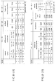
- FIG. 20 (A) composed of a bit-line B11 and a memory cell M1 with a transistor Q1 and a memory capacitor C1.
- Cb as the capacitance of the bit-line B11
- Cs as the capacitance of the memory capacitor C1
- Vs as an initial potential of the node S1 of the memory cell M1
- Vh as a potential of the opposite electrode of the node S1
- a following equation is obtained when the potential of the bit-line changes from Vi to Vx by stimulating a word-line WL1.
- Vx (Cb ⁇ Vi + Cs ⁇ Vs)/(Cb + Cs)
- Vx (Cb ⁇ Vi + Cs ⁇ Vs)/(Cb + Cs)
- Vx 2.19V.
- two other initial values should be defined. When they are Vcc/3 (1.67V) and 2Vcc/3 (3.33V), the corresponding values of Vx become 2.4V and 2.6V respectively.
- FIG. 20 (B) illustrates the relation among the four values (a), (b), (c) and (d) of Vx thus obtained and the referential potentials VR1, VR2 and VR3 referred to by the sense amplifiers of the third prior example.
- the potential difference between VR1 and (b) or (c), VR2 and (a) or (b) and VR3 and (c) or (d) is about 100mV. This is an example and the values of (b) and (c) of Vs or the values of VR1, VR2 and VR3 might be shifted, but no difference can be enlarged without reducing another difference. And, to reduce the source voltage Vcc, the differences must be reduced still more.
- a primary object of the present invention is to provide a multi-valued semiconductor memory device with shorter access times including read-out times. Another important object is to provide a multi-valued semiconductor memory device having a larger operating margin for a sense amplifier even with a low source voltage.
- a semiconductor memory device of the present invention has a plurality of bit-memory units.
- Each of the bit-memory units comprises: a first and a second bit-lines; a plurality of memory cells, each of the memory cells having a memory capacitor for storing a charge which generates a differential potential between the first and the second bit-lines and is recharged with potentials of the first and the second bit-lines when a word-line is charged; at least two sets of means for generating a read-out potential, each of the at least two sets of means for generating a read-out potential having a first and a second in-out terminal and a sense amplifier which discriminates a potential difference between the first and the second in-out terminals and turns to logic '1' by charging the first in-out terminal with a potential of a positive sense amplifier activating signal and the second in-out terminals with a potential of a negative sense amplifier activating signal in case the first in-out terminal is at a higher potential than the second in-out
- the first and the second bit-lines are pre-charged with a potential of a middle reference voltage by a pre-charge circuit when a pre-charge control signal is at high level; an electrode of the memory capacitor is connected to the middle reference voltage and the other electrode of the memory capacitor is connected through a transistor to one of the first and the second bit-line when the word-line is at high level; the differential potential is transfered through the data transfer control circuit to each of the at least two sets of means for generating a read-out potential when a first and one of a second and a third transfer control signals are at high level after the word-line is turned to high level, the second transfer control signal being at high level in case the memory capacitor is connected to the first bit-line and the third transfer control signal being at high level in case the memory capacitor is connected to the second bit-line; the potential shift control signal is turned to high level after the at least two sets of means for generating a read-out potential are separated from the first and the second bit-lines by turnning the first and the one
- N sets of means for generating a read-out potential for example, N + 1 levels of a charge stored in an ordinal memory cell of a capacitor and a transistor can be discriminated by arranging properly the potential shift values of the N sets of means for generating a read-out potential.
- a read-out time equivalent to that of ordinal binary DRAMs is obtained, as the differential potential of the first and the second bit-lines generated with the memory cell is transferred to the sense amplifiers at once and sensed at which level by a cooperation of the sense amplifiers for outputting as binary data. And a memory cell refreshment is performed with a refreshing potential obtained simply by transferring the potentials generated by the sense amplifiers to the first and the second bit-lines and unifying them, providing a write time equivalent to that of ordinary DRAMs.
- the first and the second bit-lines are pre-charged with a potential of a middle reference voltage by a pre-charge circuit when a pre-charge control signal is at high level; a first electrode of the memory capacitor is connected through a transistor to the first bit-line when the word-line is at high level and a second electrode of the memory capacitor is connected through another transistor to the second bit-line when the word-line is at high level; the differential potential is transfered to each of the at least two sets of means for generating a read-out potential through the data transfer control circuit when a first and a second transfer control signals are at high level after the word-line is turned to high level; the potential shift control signal is turned to high level after the at least two sets of means for generating a read-out potential are separated from the first and the second bit-lines by turnning the first and the second transfer control signals to low level; the second transfer control signal is turned to high level for controlling the data transfer control circuit for recharging the memory capacitor after the sense amplifiers of the at least
- 4(Cb + Cs)/(Cb + Cs) times, or about 3.7 times in an example, of the potential difference for the sense amplifier can be obtained compared with the third prior example with a memory cell composed of two transistor and a capacitor driven by same source voltage, where Cb is the capacitance of a bit-line and Cs is the capacitance of a memory cell, and a still faster memory cell refreshment is performed compared with the previous embodiment as unifying operation of the potentials of the bit-lines is eliminated.
- FIG. 1 is a block diagram of a first embodiment of the invention.
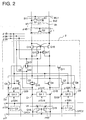
- FIG. 2 is a circuit diagram of a principal part of the embodiment of FIG. 1.
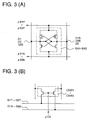
- FIG. 3 (A) is a circuit diagram of a sense amplifier in FIG. 1.
- FIG. 3 (B) is a circuit diagram of a column switch circuit in FIG. 1.
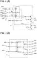
- FIG. 4 (A) is a circuit diagram of the AD converter 3 and the output buffer 4 of FIG. 1.
- FIG. 4 (B) is a circuit diagram of the input buffer 5 of FIG. 1.
- FIG. 5 illustrates wave forms and control timings of the control signals in the embodiment of FIG. 1.
- FIG. 6 illustrates an example of the wave form transitions of generated signals in the embodiment of FIG. 1.
- FIG. 7 illustrates another example of the wave form transitions of generated signals in the embodiment of FIG. 1.
- FIG. 8 illustrates second another example of the wave form transitions of generated signals in the embodiment of FIG. 1.
- FIG. 9 illustrates still another example of the wave form transitions of generated signals in the embodiment of FIG. 1.
- FIG. 10 (A) shows a first part of a table illustrating potentials of each part, logics of the sense amplifiers and a part of control of the data transfer circuit 5 in the embodiment of FIG. 1.
- FIG. 10 (B) shows the latter part of the table shown in FIG. 10 (A).
- FIG. 11 (A) shows a table illustrating relations among logics of the sense amplifiers, sets of output data and parallel binary output data in the embodiment of FIG. 1.
- FIG. 11 (B) shows a table illustrating relations among parallel binary input data, logics of the sense amplifiers, a part of control of the data transfer circuit 5 and potentials of each part in the embodiment of FIG. 1.
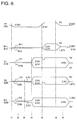
- FIG. 12 is a circuit diagram of a principal part of a second embodiment.
- FIG. 13 illustrates wave forms and control timings of the control signals in the embodiment of FIG. 12.
- FIG. 14 illustrates an example of the wave form transitions of generated signals in the embodiment of FIG. 12.
- FIG. 15 illustrates another example of the wave form transitions of generated signals in the embodiment of FIG. 12.
- FIG. 16 illustrates second another example of the wave form transitions of generated signals in the embodiment of FIG. 12.
- FIG. 17 illustrates still another example of the wave form transitions of generated signals in the embodiment of FIG. 12.
- FIG. 18 (A) shows a first part of a table illustrating potentials of each part, logics of the sense amplifiers and a part of control of the data transfer circuit 5 in the embodiment of FIG. 12.
- FIG. 18 (B) shows the latter part of the table shown in FIG. 18 (A).
- FIG. 19 (A) shows a table illustrating relations among logics of the sense amplifiers, sets of output data and parallel binary output data in the embodiment of FIG. 12.
- FIG. 19 (B) shows a table illustrating relations among parallel binary input data, logics of the sense amplifiers, a part of control of the data transfer circuit 5 and potentials of each part in the embodiment of FIG. 12.
- FIG. 20 (A) shows a memory cell with a capacitor and a transistor.
- FIG. 20 (B) shows relation among initial values Vs, differential potentials Vx and reference potentials VR1, VR2 and VR3.
- FIG. 21 is a circuit diagram of a modification of the circuit shown in FIG. 12.
- FIG. 1 is a block diagram of a first embodiment of the invention and FIG. 2 is a circuit diagram of a principal part of the embodiment.
- a pair of bit-lines is composed of a first bit-line B11 and a second bit-line B12.
- a plurality of memory cells M1 comprises a transistor Q1 for switching and a memory capacitor C1 for storing a charge, the transistor Q1 being connected between the bit-line B11 and an electrode of the memory capacitor C1 with its source and drain and also connected to a word-line WL1 with its gate, the other electrode of the memory capacitor C1 being supplied with a middle reference voltage Vh which is a half of a source voltage Vcc.
- To the bit-line B12 there are also connected plurality of memory cells M2 having the same contrivance as the memory cells M1.
- Write signals or read-out signals from/to selected one of the memory cells M1 or M2 are transferred by the two bit-lines B11 and B12.
- One of the memory cells M1 or M2 stores the signal delivered by the bit-lines B11 and B12 and sends out the stored signal to the bit-lines B11 and B12, when selected by stimulating a corresponding word-line of the word-lines WL1, WL2, ... .
- a pre-charge circuit PRE pre-charges the bit-lines B11 and B12 at an appointed timing by a pre-charge control signal ⁇ P.
- a word-line selects a memory cell and a differential potential is generated between the bit-lines B11 and B12.
- composition of the embodiment is described for the first place, assuming that a memory cell connected to the bit-line B11 is selected and the potential of the bit-line B11 is changed.
- a first sense amplifier SA1 amplifies and outputs the differential potential between the bit-lines B11 and B12 according to first sense amplifier activating signals ⁇ S1P and ⁇ S1N.
- the sense amplifier SA1 outputs a first read-out potential of the source voltage Vcc at its first in-out terminal D1 (and a fourth read-out potential 0V at its second in-out terminal D1B), or outputs the fourth read-out potential at the in-out terminal D1 when the read-out signal corresponds to one of the two lower levels (and the first read-out potential at the second in-out terminal D1B).
- Second means 62 for generating a read-out potential are composed of a second sense amplifier SA2 and a first potential shift circuit DPC1.
- a potential shift capacitor C2 of the potential shift circuit DPC1 To an electrode of a potential shift capacitor C2 of the potential shift circuit DPC1 is supplied with the potential of the bit-line B11, which is shifted to lower side by a fixed value with a potential shift control signal ⁇ DB supplied to the other electrode of the potential shift capacitor C2.
- the sense amplifier SA2 amplifies the differential potential between the shifted potential and the middle reference voltage Vh of the bit-line B12 according to second sense amplifier activating signals ⁇ S2P and ⁇ S2N.
- the input potential at a first in-out terminal D2 is so shifted as to be higher than the middle reference voltage Vh only when the potential of the bit-line B11 corresponds to the highest level of the four levels.
- the sense amplifier SA2 outputs the first read-out potential of the source voltage Vcc at the in-out terminal D2 and a third read-out potential Vcc/3 at a second in-out terminal D2B of the sense amplifier SA2 only when the potential of the bit-line B11 corresponds the highest level of the four levels, otherwise outputting the third read-out potential at the in-out terminal D2 and the first read-out potential at the in-out terminal D2B.
- Third means 63 for generating a read-out potential are composed of a third sense amplifier SA3 and a second potential shift circuit DPC2 with a potential shift capacitor C3 which shifts here the supplied potential from the bit-line B12 to lower side by a fixed value with the potential shift control signal ⁇ DB.
- the sense amplifier SA3 amplifies the differential potential between the potential supplied from the bit-line B11 and the shifted middle reference voltage according to third sense amplifier activating signals ⁇ S3P and ⁇ S3N, outputting the fourth read-out potential of 0V at the in-out terminal D3 and a second read-out potential of 2Vcc/3 at a second in-out terminal D3B only when the potential of the bit-line B11 corresponds the lowest level of the four levels, and otherwise outputting 2Vcc/3 at the in-out terminal D3 and the fourth read-out potential at the in-out terminal D3B of the sense amplifier SA3.
- An AD converter receives the read-out potentials from the first and the second in-out terminals D1 and D1B, D2 and D2B and D3 and D3B of the sense amplifiers SA1, SA2 and SA3 through column switch circuits CSW1, CSW2 and CSW3, which selects a column (a pair of bit-lines) appointed by a column select signal ⁇ CS, and through I/O data busses IO1T, IO1B, IO2T, IO2B, IO3T and IO3B.
- the AD converter 3 outputs three data R1, R2 and R3, the data R1 being at logic '1' when the first in-out terminal D1 of the sense amplifier SA1 is at the first read-out potential and otherwise at logic '0', the data R2 being at logic '1' when the first in-out terminal D2 of the sense amplifier SA2 is at the first read-out potential and otherwise at logic '0', and the data R3 being at logic '0' when the first in-out terminal D3 of the sense amplifier SA3 is at the fourth read-out potential and otherwise at logic '1'.
- An output buffer circuit 4 receives the data R1, R2 and R3 from the AD converter and outputs the data R1 to a first I/O terminal IOT1, and to a second I/O terminal IOT2, the data R2 when the logic of the data R1 is '1', or the data R3 when the logic of the data R1 is '0'.
- Means for generating a refreshing potential are composed of a data transfer control circuit 2 and a bit-line balancing circuit 1.
- the date transfer circuit 2 has transistors Q3 to Q17.
- the transistors Q3 to Q8 and transistors Q10 and Q14 to Q17 are for controlling signal transfer from the bit-lines B11 and B12 to the in-out terminals D1 and D1B, D2 and D2B and D3 and D3B of the sense amplifiers SA1, SA2 and SA3, or vice versa, according to transfer control signals ⁇ 1B, ⁇ 2B and ⁇ 3B.
- the transistors Q4 to Q8 are controlled by the transfer control signal ⁇ 1B
- the transistors Q10, Q12, Q14 and Q16 are controlled by the transfer control signal ⁇ 2B
- the transistors Q10, Q13, Q15 and Q17 are controlled by the transfer control signal ⁇ 3B.
- the transistors Q9 and Q11 are controlled by potentials of the in-out terminal D1 and D1B respectively of the sense amplifier SA1.
- the data transfer circuit 2 transfers the signal potentials of the bit-lines B11 and B12 to the three sense amplifiers SA1, SA2 and SA3, and it transfers the amplified potentials from the sense amplifiers to the bit-lines B11 and B12 as follows.
- the potential at the first in-out terminal D1 of the sense amplifier SA1 is transferred to the bit-line B11. And to the bit-line B12, the potential at the first in-out terminal D2 of the sense amplifier SA2 is transferred when the potential at the in-out terminal D1 is at the first read-out potential of Vcc, while the potential at the first in-out terminal D3 of the sense amplifier SA3 being transferred when the in-out terminal D1 is at the fourth read-out potential of 0V.
- the bit-lines B11 and B12 are connected for unifying the two read-out potentials to obtain a write potential to be stored at the node S1 of the selected memory cell at an appointed timing by the bit-line balancing circuit 1 having a transistor Q2 connected to the bit-lines B11 and B12 with its source and drain and controlled by a control signal ⁇ 4B supplied to its gate.
- Means for buffering and DA converting input data are composed of an input buffer 5 and the sense amplifiers SA1, SA2 and SA3.
- the input buffer 5 transfers parallel binary input data from the first I/O terminal IOT1 to the sense amplifier SA1 through the I/O data busses IO1T and IO1B and the column switch circuit CSW1, and data input from the second I/O terminal IOT2 to the sense amplifiers SA2 and SA3 through the I/O data busses IO2T, IO2B, IO3T and IO3B and the column switch circuit CSW2 and CSW3.
- the sense amplifiers SA1, SA2 and SA3 According to the binary input data, the sense amplifiers SA1, SA2 and SA3 generate a first, a second, a third or a fourth write potentials, which correspond to the first, the second, the third and the fourth read-out potentials respectively and two of them unified are supplied to the selected memory cell.
- each of the sense amplifiers SA1, SA2 and SA3 has a CMOS flip-flop type circuit as shown in FIG. 3 (A) for example, and each of the column switch circuits CSW1, CSW2 and CSW3 has a simple circuitry as shown in FIG. 3 (B).
- a circuitry of the AD converter circuit 3 and the output buffer 4 are shown in FIG. 4 (A) and a circuitry of the input buffer 5 is shown in FIG. 4 (B).
- FIG. 5 illustrates control timings of the control signals
- FIG. 6 illustrating the wave form transitions of the generated signals.
- the transfer control signals ⁇ 1B to ⁇ 3B, the control signal ⁇ 4B and the potential shift signal ⁇ DB remains at high levels.
- the potentials of the sense amplifier activating signals ⁇ S1P, ⁇ S1N, ..., ⁇ S3P and ⁇ S3N being a half (2.5V) of the source voltage Vcc (5V)
- the bit-lines B11 and B12 and the first and the second in-out terminals of the sense amplifiers SA1, SA2 and SA3 are all maintained at the middle reference voltage Vh. It is assumed here that an initial value Vs is stored at a node S1 of a memory cell connected to the bit-line B11.
- Capacitances of the bit-lines and the memory cells and so, differential potentials generated by stimulating a word-line will be described as having same values as described in connection with the third prior example and FIG. 20 (A) and FIG. 20 (B), FIG. 6 showing wave form transitions in case when the initial value Vs at the node S1 is 3.33V which corresponds to (b) in FIG. 20 (B).
- the pre-charge control signal ⁇ P, the transfer control signal ⁇ 3B and the control signal ⁇ 4B changes their status from the high levels (called H-levels) to a low level (called a L-level) of 0V, for preparing for a selection by a word-line.
- the transfer control signals ⁇ 1B and ⁇ 2B are shifted from H-level to L-level for cutting the bit-lines B11 and B12 from the sense amplifiers SA1, SA2 and SA3 electrically.
- the potential shift control signal ⁇ DB is changed from 5V to 0V for shifting the differential potentials at the in-out terminals D2 and D3B of the second and the third sense amplifiers SA2, SA3.
- the capacitance Cr of the capacitor C2 and C3 is prepared as follows.
- the potential (2.6V) at the first in-out terminal D2 of the sense amplifier SA2 should be shifted to a lower voltage (2.4V, corresponding Vx of (c) in FIG. 20) by one level of the four levels to be discriminated by the sense amplifier SA2 comparing with the middle reference voltage Vh at the second in-out terminal D2B.
- Cr Cd/ ⁇ 5/(Vj - Vy) - 1 ⁇
- Vj 2.6V
- Vy 2.4V
- Cd 30fF
- the sense amplifier 2 is able to decide only the highest level (a) (in FIG. 20 (B)) as logic '1', and others as logic '0'.
- the sense amplifier SA3 can decide the levels (a), (b) and (c) as logic '1' and only the level (d) as logic '0'.
- the potentials at each in-out terminal are 2.6V at D1, 2.5V at D1B, 2.4V at D2, 2.5V at D2B, 2.6V at D3 or 2.3V at D3B. Therefore, when the sense amplifiers SA1, SA2 and SA3 are activated at the timing t4, the in-out terminals D1, D2B and D3 become at H-levels, the in-out terminals D1B, D2 and D3B at L-levels.
- the sense amplifier activating signals all having initial values 2.5V, ⁇ S1P changes to 5V, ⁇ S1N changes to 0V, ⁇ S2P changes to 5V, ⁇ S2N changes to 1.67V, ⁇ S3P changes to 3.33V and ⁇ S3N changes to 0V. Therefore, the amplified potential of the in-out terminal D1 becomes 5V a time after the timing t4, while D1B 0V, D2 1.67V, D2B 5V, D3 3.33V and D3B 0V.
- the bit-line B12 is connected to either of the in-out terminal D2 or D3 through the NMOS type transistors Q9 to Q17.
- the in-out terminal D2 is connected to the bit-line B12 through the transistor Q9 and Q12, since the transistor Q11 controled by the potential of the in-out terminal D1B remains OFF because of the L-level of the in-out terminal D1B and the transistor Q15 and Q17 remain OFF among the transistors Q14, Q15, Q16 and Q17 controlled by the transfer control signals ⁇ 2B and ⁇ 3B because of the L-level of the transfer control signal ⁇ 3B.
- the potentials of the bit-lines B11 and B12 remaining unstable because of the selection of the word-line just after the timing t5 when the transfer control signal ⁇ 2B is turned to H-level, the potential of the bit-line B11 finally becomes 5V, which is the potential of the sense amplifier activating signal ⁇ S1P, and the potential of the bit-line B12 finally becomes 1.67V, which is the potential of the sense amplifier activating signal ⁇ S3N.
- the transfer control signal ⁇ 2B is returned to L-level and the control signal ⁇ 4B is returned to H-level, for separating the bit-lines B11 and B12 from the sense amplifiers SA1, SA2 and SA3 and connecting them to each other. Since the bit-line B11 and B12 have same capacitances and are charged with 5V and 1.67V respectively, the potential of the bit-lines B11 and B12 and consequently the potential of the node S1 of the selected memory cell becomes 3.33V.
- the potentials of the bit-lines B11 and B12, the in-out terminals D1, D1B, D2, D2B, D3 and D3B are returned to the standby status of 2.5V by returning the transfer control signals ⁇ 1B, ⁇ 2B and ⁇ 3B and the pre-charge control signal ⁇ P to H-levels and returning the sense amplifier activating signals to 2.5V.
- the column select signal ⁇ CS becomes at H-level, and the first, the second, the third and the fourth read-out potentials generated by the sense amplifiers SA1, SA2 and SA3 are transfered for AD converting to the AD converter 3 through the column switch circuits CSW1, CSW2 and CSW3 and through the data I/O busses IO1T, IO1B, ..., IO3T and IO3B.
- the AD converter 3 outputs a set of three out-put data R1, R2 and R3, the data R1 being at logic '1' when the logic of the sense amplifier SA1 is '1' and otherwise at logic '0', the data R2 being at logic '1' when the logic of the sense amplifier SA2 is '1' and otherwise at logic '0', and the data R3 being at logic '0' when the logic of the sense amplifier is '0' and otherwise at logic '1'.
- the data R1 is output. From the second I/O terminal IOT2 the data R2 is output when the logic of the data R1 is '1', or the data R3 when the logic of the data R1 is '0'.
- a pair of parallel binary output data corresponding to a level of the four levels storable in a memory cell is obtained as shown in FIG. 11 (A).
- FIG. 11 (B) the relation among data logics and potentials at each part of the embodiment is tabled when a pair of parallel binary input data is written and stored as one of the four levels in one of the memory cells M1 and M2.
- the operations being apparent from the descriptions concerning to the means for buffering and DA converting and to the means for generating a refreshing potential, the detailed descriptions thereof are omitted.
- a read-out time equivalent to that of ordinary binary DRAMs is obtained, as signal potentials of the bit-lines B11 and B12 read-out from a memory cell are transferred to the three sense amplifiers SA1, SA2 and SA3 at once and sensed at which level of the four levels by a cooperation of the three sense amplifiers for outputting as a pair of parallel binary output data. And a memory cell refreshment is performed with a refreshing potential obtained simply by transferring the read-out potentials to the bit-lines B11 and B12 and unifying them.
- FIG. 12 is a circuit diagram illustrating a principal part of a second embodiment of the present invention.
- each of memory cells M1a, M2a, ... is a 2-transistor-1-capacitor type memory cell comprising a first transistor Q1a connected between a first bit-line B11 and an electrode of a memory capacitor C1 with its source and drain and connected to a word-line WL1 with its gate, and a second transistor Q1b connected between a second bit-line B12 and another electrode of the memory capacitor C1 with its source and drain and connected to the word-line WL1 with its gate.
- First means 61 for generating a read-out potential comprises a first sense amplifier SA1.
- the sense amplifier SA1 compares signal potentials rea-out and transfered to the bit-lines B11 and B12 with the four levels for generating a first read-out potential of 5V at its first in-out terminal D1 connected to the bit-line B11 and a fourth read-out potential of 0V at its second in-out terminal D1B connected to the bit-line B12 when the potential of the bit-line B11 is higher than the potential of the bit-line B12, that means the read-out differencial potential corresponds to one of higher two levels of the four levels, or generating the fourth read-out potential at its first in-out terminal D1 and the first read-out potential at the in-out terminal D1B when the potential of the bit-line B11 is lower than the potential of the bit-line B12.
- Second and third means 62 and 63 for generating a read-out potential comprise a first potential shift circuit DPC1a, a second sense amplifier SA2, a second potential shift circuit DPC2a and a third sense amplifier SA3 respectively.
- the first potential shift circuit DPC1a receives and shifts the signal potential read-out and generated at the bit-line B11 beforehand pre-charged by the pre-charge circuit PRE to lower side by a fixed value.
- the second sense amplifier SA2 compares the shifted potential by the potential shift circuit DPC1a with the potential of the bit-line B12 for generating a fourth read-out potential of 0V at its second inout terminal D2B connected to the bit-line B12 when the potential of the bit-line B12 is lower than the shifted potential, that means the read-out differential potential corresponds to the highest level of the four levels, or generating the second read-out potential of 3.33V at the in-out terminal D2B when the potential of the bit-line B12 is higher, that means the read-out differential potential corresponds to one of the three levels other than the highest level.
- the second potential shift circuit DPC2a receives and shifts the signal potential read-out and generated at the bit-line B12 beforehand pre-charged by the pre-charge circuit PRE to lower side by a fixed value.
- the sense amplifier SA3 compares the shifted potential by the potential shift circuit DPC2a with the potential of the bit-line B11 for generating a first read-out potential of 5V at its second in-out terminal D3B connected to the bit-line B12 when the potential of the bit-line B11 is lower than the shifted potential, that means the read-out differential potential corresponds to the lowest level of the four levels, or generating the third read-out potential of 1.67V at the in-out terminal D3B when the potential of the bit-line B11 is higher, that means the read-out differential potential corresponds to one of the three levels other than the lowest level.
- Means for generating a refreshing potential are a part of a data transfer control circuit 2a comprising transistors Q3 to Q12.
- the transistor Q3 transfers the potential at the in-out terminal D1 of the sense amplifier SA1 as a first write potential to the bit-line B11.
- the transistors Q9, Q10, Q11 and Q12 transfer the potential at the in-out terminal D2B of the sense amplifier SA2 as a second write potential to the bit-line B12 when the potential at the first in-out terminal D1 of the sense amplifier SA1 is the first read-out potential of 5V, or the potential at the second in-out terminal D3B of the sense amplifier SA3 as the second write potential to the bit-line B12 when the potential at the in-out terminal D1 is the fourth read-out potential of 0V.
- the transistors Q3 to Q8 are for controlling signal transfer from the bit-lines B11 and B12 to the in-out terminals D1 and D1B, D2 and D2B and D3 and D3B of the sense amplifiers SA1, SA2 and SA3, transistor Q3 being used also for transferring the first write potential as described.
- the differential potentials obtained between the bit-lines B11 and B12 are calculated.
- the value of the floating capacitance of each bit-line is Cb and the capacitance of the memory capacitor C1 is Cs for a comparison with the third prior example, where Cb is a sum total of the gate capacitances of MOS transistors in the sense amplifiers, lead line capacitances to the in-out terminals of the sense amplifiers, diffusion capacitances of the transistor Q3 or Q4 and so on as same as other binary or multi-valued DRAMs.
- the potentials of the bit-line B11 and B12 being both Vh and the potentials of two nodes (two electrodes of the memory capacitor C1) S1 and S2 of a memory cell being Vs1 and Vs2 respectively, when the potentials of the bit-line B11 and B12 is changed to Vx1 and Vx2 by selecting the memory cell by a word-line, following two equations are obtained from total charges of both B11 side and B12 side before and after the selection.
- FIG. 13 and FIG. 14 illustrating control timings of the transfer control signals and the wave form transitions in case when the differential potential corresponds to the second lowest level of the four levels (the case ⁇ in FIG. 18 (A)) of the generated signals respectively.
- bit-lines B11 and B12 and the first and second in-out terminals D1, D1B, ..., D3 and D3B of the sense amplifiers SA1, SA2 and SA3 are all maintained at the middle reference voltage Vh (2.5V) by the pre-charge circuit PRE, the potentials Vs1 and Vs2 (initial values) at the nodes S1 and S2 of a memory cell being 0V and 1.67V.
- the pre-charge control signal ⁇ P is changed from H-level to L-level for preparing for a selection by a word-line.
- the transfer control signals ⁇ 1B and ⁇ 2B are shifted from H-level to L-level for cutting the bit-lines B11 and B12 from the sense amplifiers SA1, SA2 and SA3 electrically.
- the potential shift control signal ⁇ DB is changed from 5V to 0V for shifting the differential potentials at the first in-out terminal D2 and the second in-out terminal D3B of the second and the third sense amplifiers SA2 and SA3.
- the capacitance Cr of the potential shift capacitor C2 and C3 of the potential shift circuits DPC1a and DPC2a is prepared as follows.
- the potentials at the in-out terminal D2 is shifted so that the second highest value at the in-out terminal D2 (2.68V, the value in case ⁇ in FIG. 18 (A)) be shifted to the lowest value at the in-out terminal D2B (1.95V, the value in case ⁇ in FIG. 18 (A)), for the sense amplifier SA2 discriminating only the highest level of the differential potential (the case ⁇ in FIG. 18 (A)) as logic '1' and otherwise as logic '0'.
- the capacitance Cr is set to the value obtained as follows.
- the sense amplifier SA3 can decide only the lowest level (the case ⁇ in FIG. 18 (A)) of the four levels of the differential potential as logic '0', and other levels as logic '1'.
- the potentials at each in-out terminal are 2.31V at D1, 2.68V at D1B, 1.57V at D2, 2.68V at D2B, 2.31V at D3 or 1.95V at D3B. Therefore, when the sense amplifiers SA1, SA2 and SA3 are activated, the in-out terminals D1, D2 and D3B become at L-levels, the in-out terminals D1B, D2B and D3 at H-levels.
- the sense amplifier activating signals all having initial values 2.5V, ⁇ S1P and ⁇ S3P change to 5V, ⁇ S1N and ⁇ S2N change to 0V, ⁇ S2P changes to 3.33V, and ⁇ S3N changes to 1.67V. Therefore, the amplified potential of the in-out terminal D1 becomes 0V a time after the timing t4, while D1B and D3 5V, D2 0V, D2B 3.33V and D3B 1.67V.
- the bit-line B12 is connected to either of the in-out terminal D2B or D3B through the transistors Q9 to Q12.
- the in-out terminal D3B is connected to the bit-line B12 through the transistor Q11 and Q12, since the transistor Q9 remains OFF.
- the potentials of the bit-lines B11 and B12 remaining unstable because of the selection of the word-line WL1 just after the timing t5 when the transfer control signal ⁇ 2B is turned to H-level, the potential of the bit-line B11 finally becomes 0V, which is the potential at the in-out terminal D1 of the sense amplifier SA1, and the potential of the bit-line B12 finally becomes 1.67V, which is the potential at the in-out terminal D3B of the sens amplifier SA3.
- the transfer control signals ⁇ 1B and the pre-charge control signal ⁇ P is returned to H-levels and the sense amplifier activating signals ⁇ S1P, ⁇ S1N, ..., ⁇ S3P and ⁇ S3N are returned to 2.5V, for returning the potentials of the bit-lines B11 and B12 and the in-out terminals of the sense amplifiers SA1, SA2 and SA3 to the middle referencial voltage of 2.5V.
- FIG. 15 The wave form transitions of generated signals in other three cases ⁇ , ⁇ and ⁇ of the four cases corresponding to the four levels are shown in FIG. 15, FIG. 16 and FIG. 17.
- FIG. 18 (A) and FIG. 18 (B) The wave form transitions of generated signals in other three cases ⁇ , ⁇ and ⁇ of the four cases corresponding to the four levels are shown in FIG. 15, FIG. 16 and FIG. 17.
- FIG. 18 (A) and FIG. 18 (B) The wave form transitions of generated signals in other three cases ⁇ , ⁇ and ⁇ of the four cases corresponding to the four levels are shown in FIG. 15, FIG. 16 and FIG. 17.
- FIG. 18 (A) and FIG. 18 (B) The wave form transitions of generated signals in other three cases ⁇ , ⁇ and ⁇ of the four cases corresponding to the four levels are shown in FIG. 15, FIG. 16 and FIG. 17.
- FIG. 18 (B) The wave form transitions of generated signals in other three cases ⁇ , ⁇ and ⁇ of the four cases corresponding
- the data output or the data input of the embodiment is performed in the same way as the first embodiment, and detailed descriptions are also omitted.
- the relation among data logics and potentials at each part of the embodiment is tabled in FIG. 19 (A) and in FIG. 19 (B).
- a potential differnce Def1 between the highest level and the lowest level of the differential potential in the first embodiment, or the third prior example is calculated as folllows from the equation (1).
- a potential difference Def2 between the highest level and the lowest level is represented as follows from the equation (4).
- Still anoter merit is that the write times are still shotened as the bit-line balancing is not necessary in the second embodiment.
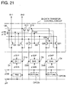
- FIG. 21 is a circuit diagram of a modification of the circuit shown in FIG. 12 for discriminating five valued information stored between the node S1 and the node S2.
- the modified circuit further comprises a fourth sense amplifier SA4 activated with sense amplifier signals ⁇ S4P and ⁇ S4N, a third potential shift circuit DPC3b composed of a potential shift capacitor C4b, transistors Q20 and Q21 controlled with the transfer control signal ⁇ 1B for connecting in-out terminals D4 and D4B of the sense amplifier SA4 to the bit-lines B11 and B12, a transistor Q22 for connecting the in-out terminal D3B to the bit-line B12 when logic of the sense amplifier SA4 is '1', and a transistor Q23 diode connected for connecting the bit-line B12 to the in-out terminal D4B when the sense amplifier SA4 is at logic '0'.
- the potential of the bit-line B11 becomes 2.13V and the potential of the bit-line B12 becomes 2.87V when a memory cell at the fifth level is selected.
- the potential at the second in-out terminal D3B of the sense amplifier SA3 is shifted by 0.56V to lower side and the potential at the second in-out terminal D4B of the sense amplifier SA4 is shifted by 0.92V to lower side.
- the capacitances of the potential shift capacitors C3b and C4b are set to about 3.8fF and 6.8fF respectively.
- the sense amplifier SA3 becomes logic '0' when the differential potential is at the fifth level (-0.74V) or the fourth level (-1.10V, ⁇ in FIG. 18 (A)) and otherwise becomes logic '1', while the sense amplifier SA4 becomes logic '0' only when the differential potential is at the fourth level.
- first embodiment and the second embodiment of the invention are both applicable for DRAMs with memory cells storing any valued information by adding sense amplifiers, arranging the capacitances of the potential shift capacitors and preparing potentials of sense amplifier activating signals in a similar way, on condition that a sufficient differential potential is secured, although levels of differential potentials should be better divided equally into 2 n levels in consideration for an interface with binary data.
Landscapes
- Engineering & Computer Science (AREA)
- Computer Hardware Design (AREA)
- Microelectronics & Electronic Packaging (AREA)
- Dram (AREA)
Applications Claiming Priority (3)
| Application Number | Priority Date | Filing Date | Title |
|---|---|---|---|
| JP32266194 | 1994-12-26 | ||
| JP322661/94 | 1994-12-26 | ||
| JP6322661A JPH08180688A (ja) | 1994-12-26 | 1994-12-26 | 半導体記憶装置 |
Publications (3)
| Publication Number | Publication Date |
|---|---|
| EP0720174A2 true EP0720174A2 (fr) | 1996-07-03 |
| EP0720174A3 EP0720174A3 (fr) | 1998-01-21 |
| EP0720174B1 EP0720174B1 (fr) | 2000-10-04 |
Family
ID=18146195
Family Applications (1)
| Application Number | Title | Priority Date | Filing Date |
|---|---|---|---|
| EP95120254A Expired - Lifetime EP0720174B1 (fr) | 1994-12-26 | 1995-12-21 | Dispositif de mémoire à semi-conducteurs à multi-états |
Country Status (5)
| Country | Link |
|---|---|
| US (1) | US5610855A (fr) |
| EP (1) | EP0720174B1 (fr) |
| JP (1) | JPH08180688A (fr) |
| KR (2) | KR960025780A (fr) |
| DE (1) | DE69519015T2 (fr) |
Cited By (1)
| Publication number | Priority date | Publication date | Assignee | Title |
|---|---|---|---|---|
| EP0851427A3 (fr) * | 1996-12-23 | 1999-07-14 | Lsi Logic Corporation | Système de mémoire ayant un capteur sur puce de température pour réguler le débit de rafraíchissement d'un réseau de mémoire DRAM |
Families Citing this family (5)
| Publication number | Priority date | Publication date | Assignee | Title |
|---|---|---|---|---|
| KR100224769B1 (ko) * | 1995-12-29 | 1999-10-15 | 김영환 | 고속 버스트 리드/라이트 동작에 적합한 데이타 버스 라인 구조를 갖는 반도체 메모리 장치 |
| US8339159B2 (en) | 2008-08-13 | 2012-12-25 | Hynix Semiconductor Inc. | Input buffer circuit of semiconductor apparatus |
| KR101053524B1 (ko) | 2009-06-08 | 2011-08-03 | 주식회사 하이닉스반도체 | 반도체 버퍼 회로 |
| KR20160074826A (ko) | 2014-12-18 | 2016-06-29 | 삼성전자주식회사 | 반도체 장치 |
| CA3030723C (fr) | 2019-01-21 | 2024-06-04 | Mitchell B. Miller | Systeme et procede de stockage, de traitement et de transmission des renseignements electriques bidirectionnels |
Citations (3)
| Publication number | Priority date | Publication date | Assignee | Title |
|---|---|---|---|---|
| JPS6295796A (ja) | 1985-10-21 | 1987-05-02 | Hitachi Ltd | 半導体多値記憶装置 |
| JPS63195896A (ja) | 1987-02-06 | 1988-08-12 | Mitsubishi Electric Corp | 多値記憶ダイナミツクram装置 |
| JPH01196791A (ja) | 1988-02-02 | 1989-08-08 | Toshiba Corp | 半導体記憶装置 |
Family Cites Families (4)
| Publication number | Priority date | Publication date | Assignee | Title |
|---|---|---|---|---|
| US4719600A (en) * | 1986-02-18 | 1988-01-12 | International Business Machines Corporation | Sense circuit for multilevel storage system |
| JPS63149900A (ja) * | 1986-12-15 | 1988-06-22 | Toshiba Corp | 半導体メモリ |
| JPH01171194A (ja) * | 1987-12-25 | 1989-07-06 | Nec Ic Microcomput Syst Ltd | 半導体記憶装置 |
| JP2573416B2 (ja) * | 1990-11-28 | 1997-01-22 | 株式会社東芝 | 半導体記憶装置 |
-
1994
- 1994-12-26 JP JP6322661A patent/JPH08180688A/ja active Pending
-
1995
- 1995-12-21 DE DE69519015T patent/DE69519015T2/de not_active Expired - Fee Related
- 1995-12-21 EP EP95120254A patent/EP0720174B1/fr not_active Expired - Lifetime
- 1995-12-21 US US08/576,574 patent/US5610855A/en not_active Expired - Fee Related
- 1995-12-26 KR KR1019950072155A patent/KR960025780A/ko active Granted
- 1995-12-26 KR KR1019950072155A patent/KR100226951B1/ko not_active Expired - Fee Related
Patent Citations (3)
| Publication number | Priority date | Publication date | Assignee | Title |
|---|---|---|---|---|
| JPS6295796A (ja) | 1985-10-21 | 1987-05-02 | Hitachi Ltd | 半導体多値記憶装置 |
| JPS63195896A (ja) | 1987-02-06 | 1988-08-12 | Mitsubishi Electric Corp | 多値記憶ダイナミツクram装置 |
| JPH01196791A (ja) | 1988-02-02 | 1989-08-08 | Toshiba Corp | 半導体記憶装置 |
Cited By (1)
| Publication number | Priority date | Publication date | Assignee | Title |
|---|---|---|---|---|
| EP0851427A3 (fr) * | 1996-12-23 | 1999-07-14 | Lsi Logic Corporation | Système de mémoire ayant un capteur sur puce de température pour réguler le débit de rafraíchissement d'un réseau de mémoire DRAM |
Also Published As
| Publication number | Publication date |
|---|---|
| DE69519015T2 (de) | 2001-02-15 |
| KR960025780A (ko) | 1996-07-20 |
| EP0720174B1 (fr) | 2000-10-04 |
| JPH08180688A (ja) | 1996-07-12 |
| KR100226951B1 (ko) | 1999-10-15 |
| DE69519015D1 (de) | 2000-11-09 |
| EP0720174A3 (fr) | 1998-01-21 |
| US5610855A (en) | 1997-03-11 |
Similar Documents
| Publication | Publication Date | Title |
|---|---|---|
| US5828611A (en) | Semiconductor memory device having internal voltage booster circuit coupled to bit line charging/equalizing circuit | |
| US5293563A (en) | Multi-level memory cell with increased read-out margin | |
| KR910006112B1 (ko) | 다수값 정보기억방식의 반도체기억장치 | |
| JPS60242592A (ja) | 金属酸化膜半導体ダイナミック・ランダム アクセス・メモリ | |
| JP4583703B2 (ja) | 半導体記憶装置 | |
| US5475642A (en) | Dynamic random access memory with bit line preamp/driver | |
| KR100284468B1 (ko) | Dram의글로벌비트라인을이용한싱글-엔드센싱 | |
| JPH04219698A (ja) | ダイナミック型半導体記憶装置 | |
| US6049493A (en) | Semiconductor memory device having a precharge device | |
| US5208773A (en) | Semiconductor memory device having bit lines and word lines different in data reading and data writing | |
| EP0720174B1 (fr) | Dispositif de mémoire à semi-conducteurs à multi-états | |
| US4991142A (en) | Dynamic random access memory with improved sensing and refreshing | |
| US5329479A (en) | Dynamic semiconductor memories | |
| KR100231404B1 (ko) | 다수의 값을 갖는 소형 반도체 메모리 디바이스 | |
| US4858193A (en) | Preamplification method and apparatus for dram sense amplifiers | |
| JPH04219689A (ja) | 半導体記憶装置およびその読出方法 | |
| JP2011222091A (ja) | 半導体装置及び情報処理システム | |
| JPS5935114B2 (ja) | 増巾回路 | |
| JPS63195896A (ja) | 多値記憶ダイナミツクram装置 | |
| JP2622179B2 (ja) | ダイナミック型半導体記憶装置 | |
| US6018486A (en) | Reading method and circuit for dynamic memory | |
| JPS60258793A (ja) | ダイナミック型半導体記憶装置 | |
| EP0920029A2 (fr) | Mémoire RAM multi-étâts | |
| KR100218305B1 (ko) | 분산형 센스앰프를 갖는 디램 | |
| KR100351690B1 (ko) | 다중값 메모리셀들을 갖는 반도체메모리장치 |
Legal Events
| Date | Code | Title | Description |
|---|---|---|---|
| PUAI | Public reference made under article 153(3) epc to a published international application that has entered the european phase |
Free format text: ORIGINAL CODE: 0009012 |
|
| AK | Designated contracting states |
Kind code of ref document: A2 Designated state(s): DE FR GB |
|
| PUAL | Search report despatched |
Free format text: ORIGINAL CODE: 0009013 |
|
| AK | Designated contracting states |
Kind code of ref document: A3 Designated state(s): DE FR GB |
|
| 17P | Request for examination filed |
Effective date: 19971210 |
|
| GRAG | Despatch of communication of intention to grant |
Free format text: ORIGINAL CODE: EPIDOS AGRA |
|
| 17Q | First examination report despatched |
Effective date: 19990917 |
|
| GRAG | Despatch of communication of intention to grant |
Free format text: ORIGINAL CODE: EPIDOS AGRA |
|
| GRAG | Despatch of communication of intention to grant |
Free format text: ORIGINAL CODE: EPIDOS AGRA |
|
| GRAH | Despatch of communication of intention to grant a patent |
Free format text: ORIGINAL CODE: EPIDOS IGRA |
|
| GRAH | Despatch of communication of intention to grant a patent |
Free format text: ORIGINAL CODE: EPIDOS IGRA |
|
| GRAH | Despatch of communication of intention to grant a patent |
Free format text: ORIGINAL CODE: EPIDOS IGRA |
|
| GRAA | (expected) grant |
Free format text: ORIGINAL CODE: 0009210 |
|
| AK | Designated contracting states |
Kind code of ref document: B1 Designated state(s): DE FR GB |
|
| REF | Corresponds to: |
Ref document number: 69519015 Country of ref document: DE Date of ref document: 20001109 |
|
| ET | Fr: translation filed | ||
| PLBE | No opposition filed within time limit |
Free format text: ORIGINAL CODE: 0009261 |
|
| STAA | Information on the status of an ep patent application or granted ep patent |
Free format text: STATUS: NO OPPOSITION FILED WITHIN TIME LIMIT |
|
| 26N | No opposition filed | ||
| PGFP | Annual fee paid to national office [announced via postgrant information from national office to epo] |
Ref country code: FR Payment date: 20011212 Year of fee payment: 7 |
|
| PGFP | Annual fee paid to national office [announced via postgrant information from national office to epo] |
Ref country code: GB Payment date: 20011219 Year of fee payment: 7 |
|
| REG | Reference to a national code |
Ref country code: GB Ref legal event code: IF02 |
|
| PGFP | Annual fee paid to national office [announced via postgrant information from national office to epo] |
Ref country code: DE Payment date: 20020109 Year of fee payment: 7 |
|
| PG25 | Lapsed in a contracting state [announced via postgrant information from national office to epo] |
Ref country code: GB Free format text: LAPSE BECAUSE OF NON-PAYMENT OF DUE FEES Effective date: 20021221 |
|
| PG25 | Lapsed in a contracting state [announced via postgrant information from national office to epo] |
Ref country code: DE Free format text: LAPSE BECAUSE OF NON-PAYMENT OF DUE FEES Effective date: 20030701 |
|
| GBPC | Gb: european patent ceased through non-payment of renewal fee |
Effective date: 20021221 |
|
| PG25 | Lapsed in a contracting state [announced via postgrant information from national office to epo] |
Ref country code: FR Free format text: LAPSE BECAUSE OF NON-PAYMENT OF DUE FEES Effective date: 20030901 |
|
| REG | Reference to a national code |
Ref country code: FR Ref legal event code: ST |