EP0720260A1 - Gettergehäuse für eine elektronische Packung - Google Patents
Gettergehäuse für eine elektronische Packung Download PDFInfo
- Publication number
- EP0720260A1 EP0720260A1 EP95119163A EP95119163A EP0720260A1 EP 0720260 A1 EP0720260 A1 EP 0720260A1 EP 95119163 A EP95119163 A EP 95119163A EP 95119163 A EP95119163 A EP 95119163A EP 0720260 A1 EP0720260 A1 EP 0720260A1
- Authority
- EP
- European Patent Office
- Prior art keywords
- getter
- package
- enclosure
- housing
- laser
- Prior art date
- Legal status (The legal status is an assumption and is not a legal conclusion. Google has not performed a legal analysis and makes no representation as to the accuracy of the status listed.)
- Granted
Links
Images

Classifications
-
- H—ELECTRICITY
- H01—ELECTRIC ELEMENTS
- H01S—DEVICES USING THE PROCESS OF LIGHT AMPLIFICATION BY STIMULATED EMISSION OF RADIATION [LASER] TO AMPLIFY OR GENERATE LIGHT; DEVICES USING STIMULATED EMISSION OF ELECTROMAGNETIC RADIATION IN WAVE RANGES OTHER THAN OPTICAL
- H01S5/00—Semiconductor lasers
- H01S5/02—Structural details or components not essential to laser action
- H01S5/024—Arrangements for thermal management
-
- H—ELECTRICITY
- H10—SEMICONDUCTOR DEVICES; ELECTRIC SOLID-STATE DEVICES NOT OTHERWISE PROVIDED FOR
- H10H—INORGANIC LIGHT-EMITTING SEMICONDUCTOR DEVICES HAVING POTENTIAL BARRIERS
- H10H20/00—Individual inorganic light-emitting semiconductor devices having potential barriers, e.g. light-emitting diodes [LED]
- H10H20/80—Constructional details
- H10H20/85—Packages
- H10H20/8506—Containers
-
- H—ELECTRICITY
- H01—ELECTRIC ELEMENTS
- H01S—DEVICES USING THE PROCESS OF LIGHT AMPLIFICATION BY STIMULATED EMISSION OF RADIATION [LASER] TO AMPLIFY OR GENERATE LIGHT; DEVICES USING STIMULATED EMISSION OF ELECTROMAGNETIC RADIATION IN WAVE RANGES OTHER THAN OPTICAL
- H01S5/00—Semiconductor lasers
- H01S5/02—Structural details or components not essential to laser action
- H01S5/022—Mountings; Housings
- H01S5/02235—Getter material for absorbing contamination
-
- H—ELECTRICITY
- H10—SEMICONDUCTOR DEVICES; ELECTRIC SOLID-STATE DEVICES NOT OTHERWISE PROVIDED FOR
- H10W—GENERIC PACKAGES, INTERCONNECTIONS, CONNECTORS OR OTHER CONSTRUCTIONAL DETAILS OF DEVICES COVERED BY CLASS H10
- H10W76/00—Containers; Fillings or auxiliary members therefor; Seals
- H10W76/40—Fillings or auxiliary members in containers, e.g. centering rings
- H10W76/42—Fillings
- H10W76/48—Fillings including materials for absorbing or reacting with moisture or other undesired substances
-
- H—ELECTRICITY
- H01—ELECTRIC ELEMENTS
- H01S—DEVICES USING THE PROCESS OF LIGHT AMPLIFICATION BY STIMULATED EMISSION OF RADIATION [LASER] TO AMPLIFY OR GENERATE LIGHT; DEVICES USING STIMULATED EMISSION OF ELECTROMAGNETIC RADIATION IN WAVE RANGES OTHER THAN OPTICAL
- H01S5/00—Semiconductor lasers
- H01S5/0014—Measuring characteristics or properties thereof
- H01S5/0021—Degradation or life time measurements
Definitions
- This invention relates to containers for electronic and optoelectronic packages such as a semiconductor lasers, and more particularly, to getter housings for such containers.
- a possible mechanism for shortened laser life in the standard package is accumulation of solid or liquid material on intensely illuminated surfaces, such as the laser front facet, lenses in the laser beam or the fiber lenses and windows.
- the surface accumulation may occur as follows. Mobile hydrocarbons from solder flux residue, cleaning solvents, contaminants in the assembly environment, or the like are present in the hermetically sealed laser container.
- a photo-reaction may occur when a hydrocarbon encounters the laser photon flux.
- the products of the photo-reaction may form a deposit on the intensely illuminated surfaces.
- Laser performance is degraded when these deposits inordinately reflect or absorb the laser light. If the deposits absorb photons, heat build up can occur, causing melting of an active or passive surface. The heat buildup may cause accelerated diffusion of dopants at or near the laser diode junction thereby destroying the junction or reducing the junction efficiency.
- oxygen in the sealed atmosphere of the package may lengthen laser life, by action of the oxygen combining with a hydrocarbon contaminant or the products of a photo-reacted hydrocarbon to prevent or remove accumulations on passive or active components in the laser enclosure, oxygen in the enclosure can form water when combined with hydrogen present in the enclosure atmosphere.
- the hydrogen may be present as a contaminant in the gas filling the enclosure or may outgas from the metal walls of the enclosure as temperature of the enclosure increases. It is known that water causes electrical shorts, corrosion or electro-migration in the electrical circuits present in the enclosure.
- a suitable cleaning agent such as isopropyl alcohol can be used to remove residues of the manufacturing process, such as solder flux.
- the getter material should be used in block form to facilitate its incorporation in the laser enclosure.
- Mechanical mounting means were preferred rather than organic materials, e.g., epoxies or glues.
- wire or spring clip or screw mounting was considered suitable, as well as mechanical solder attachment wherein, for example, through-holes are formed in the block of getter material, the getter being placed on the inside surface of the enclosure's cover, and the getter being soldered to the cover by pouring molten solder through the through-holes.
- Getter materials are subject to particulate shedding. This could cause failure of components within a shared package, e.g. by shorting of closely spaced electrical paths or by more direct damage to optoelectronic components, such as the intrusion of an absorbing particle into the emitting path of a laser diode.
- Protective packaging is required to reduce the likelihood of getter particulate shedding and/or to reduce the likelihood of device failure in the event that such shedding does occur.
- An object of the invention is to prevent damage to electronic devices such as semiconductor lasers caused by the particulate shedding of getter material. Another object is to provide an improved technique for retaining getter material within electronic and optoelectronic packages.
- a hermetically sealed electronic package comprising a hermetically sealed enclosure in which there is disposed a device that is sealed in an atmosphere.
- the device is one that can be adversely affected by the presence of an impurity in the atmosphere.
- a getter housing for enclosing a getter.
- the getter housing has at least one surface that is permeable to the impurity but which is adapted to resist the passage of particles of the getter, the getter housing completely sealing the getter from the device.
- the permeable surface of the getter housing can be formed of porous metal or sheet metal having apertures therein.
- the getter housing optionally contains a spring for retaining the getter.
- the packaged device is a semiconductor laser
- the enclosure is filled with a gaseous medium whose oxygen content is greater than 100 ppm
- the getter is effective for adsorbing or absorbing mobile hydrocarbons and water.
- Fig. 1 is a cross-sectional view of a laser enclosure incorporating a getter.
- Fig. 2 is an exploded side view showing typical components of a high power laser.
- Fig. 3 is a cross-sectional view of a porous metal getter housing.
- Fig. 4 is a cross-sectional view taken along lines 4-4 of Fig. 3.
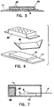
- Fig. 5 is a cross-sectional view of a further getter housing.
- Fig. 6 is an exploded view showing a modification of Fig. 5.
- Fig. 7 is a cross-sectional view of a laser enclosure incorporating yet another getter housing.
- the getter housing of the present invention is described in connection with high power laser packaging. However, this getter package is also applicable to various other kinds of electronic packaging.
- FIG. 1 shows a hermetically sealed, high power laser package or enclosure 12 including a housing 10 and cover 11.
- the high power laser 6 is fixed to substrate 2.
- the electronic devices and circuitry which are associated with the laser and typically contained in the enclosure are not shown.
- the means for coupling the laser light to a receiving device or to an optical fiber is shown as optical fiber 4.
- Other coupling means such as lenses or integrated waveguide devices may be employed as couplers.
- the laser light may be coupled to a receiving device or a waveguide located within the enclosure.
- the coupling means may allow the laser light to pass out of the enclosure through a sealed aperture.
- FIG. 2 is an illustration of the parts of a high power laser.
- the lasing body 13 is shown as having front and rear facets 14 and 15.
- the front and back facet partially reflective mirrors 20 and 18, respectively, support the lasing action. Possible mechanisms for the failure of the laser are discussed above. Briefly, photo-reactions, which may cause deposits on mirror 20 or other optical components within the enclosure, take place in the flux path beginning at mirror 20.
- the laser container is preferably filled with a gaseous medium whose oxygen content is greater than 100 ppm.
- the oxygen within the packaging atmosphere minimizes laser damage by organic impurities.
- the oxygen can react with hydrogen to form within the laser enclosure water which can adversely affect the overall operation of the electronic components within the enclosure.
- the water problem can be partially addressed by reducing the amount of hydrogen available within the enclosure for reaction with the oxygen of the oxygen-containing atmosphere.
- the metals used to form the walls of the container are pretreated; specifically, they are baked at an elevated temperature and for an extended period of time in order to substantially reduce the amount of hydrogen adsorbed or absorbed therein.
- enclosure 10 is provided with a getter 8 which acts to immobilize pre-selected type and size molecules.
- the getter is shown as a thin slab attached to the top inside surface of cover 11. Because of the typically small inside volume of the enclosure, a single getter body attached to an inside surface should be effective to immobilize the water and organic impurities which may be present.
- Getter materials must have sufficient porosity to provide them with surface area that is sufficiently great that small pieces thereof can be used to adsorb or absorb useful quantities of undesired molecules within a hermetically sealed container. Thus, such materials, especially glass and glass ceramic getter materials, are fragile and subject to particulate shedding.
- the housing of the present invention is adapted to prevent damage to components and/or prevent obstruction of light paths in the event that particulate shedding occurs.
- a preferred getter housing 26 is shown in Figs. 3 and 4.
- the housing consists of a porous metal container 28 that can be formed by pressing or electro-discharge machining.
- Container 28 can be affixed to intermediate plate 30 which can be attached to the inner surface of cover 11.
- container 28 can be affixed directly to the cover.
- the entire periphery of container 28 is preferably welded to plate 30 so that there are no gaps through which particles of getter material could pass. Any seams, such as those that occur where two sides converge to form a corner, should also be attached by welding, soldering or the like.
- Cover 11 is then affixed to housing 10.
- the resultant package 12 protects the laser and electronics from particles that might shed or flake from getter 8, thereby reducing the likelihood of device failure.
- the getter When a porous metal container is employed, the getter need not be in the form of a pellet or slab. Rather, it could be in powder or granular form, since the porous metal would prevent even powder from escaping from the getter container to the device within enclosed container 12.
- the getter housing consists of a sheet metal container 38 having a plurality of apertures 40 therethrough.
- Apertures 40 could be formed by water jet machining, laser machining, or the like. Smaller apertures are obviously preferred since they are more effective in protecting the devices within container 12 from getter particles.
- FIG. 6 A modification of the embodiment of Fig. 5 is shown in Fig. 6.
- Getter 8 is positioned on cover 11.
- a sheet metal spring 42 is placed on getter 8.
- housing 38 After housing 38 has been placed over the spring and getter and is welded to cover 11, the ends of the spring contact housing 38 and secure getter 8 to cover 11. This construction prevents the getter from shifting within the container when the package is moved or vibrated.
- Getter containers may be fixedly attached to any or all of the inside surfaces of the enclosure.
- Fig. 7 shows a getter container comprising a bent porous metal sheet 48 that is affixed to the bottom, end and two side walls of housing 10.
- a laser and other components for using the laser to provide power to an optical fiber in a fiber amplifier are packaged along with a getter in a low-hydrogen Kovar container filled with an oxygen-containing atmosphere as follows.
- the container for the laser is fabricated from Kovar plated with gold and nickel in two sections -- a body section for holding the laser and other components and a cover for carrying the getter.
- the two sections are baked in a N 2 purged oven at 150°C for 200 hours.
- the internal volume of the container is approximately 5 cm 3 .
- the getter was formed in accordance with the teachings of the aforementioned Bartholomew et al. patent application S.N. 08/320,549.
- a batch of 35 weight percent zeolite ZSM-5, 35 weight percent zeolite 4A, and about 20 weight percent porous VycorTM brand glass was dry mixed.
- Nineteen weight percent of Dow Corning silicone resin Q6-2230 was added and dry mixed into the batch. This amount was sufficient to yield about 10 weight percent silica in the finished getter.
- Dow Corning methyl cellulose at about 6 weight percent super-addition was also dry mixed into the batch. The base weight percent is taken as the combined weight of the zeolites, the porous VycorTM brand glass and the silica.
- a super-addition weight percent is calculated on the base weight but is not included in the base weight for weight percent calculations.
- An organic solvent either isopropyl alcohol or Dupont dibasic ester, and water were added to the dry mixture to produce an extrudable batch consistency.
- the plasticized batch was extruded into flat sheets, having a thickness no greater than 1 mm.
- the green body sheets were dried in air at about 85°C to 100°C for at least 3 days. Tablets were cut from these sheets with allowance for shrinkage to form finished pieces 3mm x 9mm x 1 mm after calcining at 500-620°C for a minimum of 10 hours.
- One of the tablets of getter material is enclosed in a housing formed of porous metal as described in conjunction with Figs. 3 and 4. This assembly is fastened to the inner surface of the laser package cover.
- the semiconductor laser and other components are mounted in the housing section of the package. That section along with the cover section with its attached getter are then baked for 4 hours at 300°C. Finally, the two sections are sealed together in an atmosphere of the 00.1 air product referred to above. The sealing is performed by fluxless, electrical-resistance heating.
- the semiconductor laser has been found to operate successfully over an extended period of time, i.e., for over 5000 hours, with minimal free water in the package, i.e., a water concentration in the package atmosphere of less than 5000 ppm at the end of the test period.
- the packaged high power semiconductor laser is thus suitable for use in providing power to an amplifier fiber in a fiber optic system.
Landscapes
- Physics & Mathematics (AREA)
- Condensed Matter Physics & Semiconductors (AREA)
- General Physics & Mathematics (AREA)
- Electromagnetism (AREA)
- Optics & Photonics (AREA)
- Semiconductor Lasers (AREA)
- Optical Couplings Of Light Guides (AREA)
Applications Claiming Priority (2)
| Application Number | Priority Date | Filing Date | Title |
|---|---|---|---|
| US36426494A | 1994-12-27 | 1994-12-27 | |
| US364264 | 1994-12-27 |
Publications (2)
| Publication Number | Publication Date |
|---|---|
| EP0720260A1 true EP0720260A1 (de) | 1996-07-03 |
| EP0720260B1 EP0720260B1 (de) | 2001-02-14 |
Family
ID=23433742
Family Applications (1)
| Application Number | Title | Priority Date | Filing Date |
|---|---|---|---|
| EP95119163A Revoked EP0720260B1 (de) | 1994-12-27 | 1995-12-06 | Gettergehäuse für eine optoelektronische Packung |
Country Status (7)
| Country | Link |
|---|---|
| EP (1) | EP0720260B1 (de) |
| JP (1) | JPH08236660A (de) |
| KR (1) | KR960027093A (de) |
| CN (1) | CN1132932A (de) |
| AU (1) | AU4054495A (de) |
| CA (1) | CA2162095A1 (de) |
| DE (1) | DE69520091T2 (de) |
Cited By (13)
| Publication number | Priority date | Publication date | Assignee | Title |
|---|---|---|---|---|
| US6123464A (en) * | 1999-02-10 | 2000-09-26 | The Furukawa Electric Co., Ltd. | Optical module package and method for manufacturing the same |
| US6220767B1 (en) | 1999-05-14 | 2001-04-24 | Corning Incorporated | Semiconductor laser optical waveguide telecommunications module and method of making |
| WO2001097348A1 (en) * | 2000-06-16 | 2001-12-20 | Saes Getters S.P.A. | Water getter devices for laser amplifiers and process for the manufacture thereof |
| WO2002043098A1 (en) * | 2000-11-22 | 2002-05-30 | Johnson Matthey Plc | Getters |
| US6867543B2 (en) | 2003-03-31 | 2005-03-15 | Motorola, Inc. | Microdevice assembly having a fine grain getter layer for maintaining vacuum |
| US6936354B2 (en) | 2001-09-27 | 2005-08-30 | Saes Getters S.P.A. | Systems for conversion of water into hydrogen and sorption of hydrogen in electronic devices |
| US6987304B2 (en) * | 2003-05-07 | 2006-01-17 | Honeywell International Inc. | Methods and apparatus for particle reduction in MEMS devices |
| US7534658B2 (en) | 2001-07-20 | 2009-05-19 | Saes Getters S.P.A. | Process for manufacturing microelectronic, microoptoelectronic or micromechanical devices |
| EP1675170A3 (de) * | 2004-12-22 | 2009-09-09 | Nissan Motor Company, Limited | Verpackungselemente und Verfahren zum Befestigen eines Getters |
| DE102008017553A1 (de) * | 2008-04-07 | 2009-10-08 | Siemens Aktiengesellschaft | Elektronisches System |
| EP1745513A4 (de) * | 2004-04-15 | 2010-02-24 | Getters Spa | Integrierter getter für vakuum- oder inertgas gekapselte leds |
| US8105860B2 (en) | 2001-07-20 | 2012-01-31 | Saes Getters, S.P.A. | Support with integrated deposit of gas absorbing material for manufacturing microelectronic microoptoelectronic or micromechanical devices |
| DE102005008750B4 (de) * | 2004-03-24 | 2012-02-09 | Hewlett-Packard Development Company, L.P. | Struktur zum Enthalten von Trocknungsmitteln, Verfahren zum Herstellen und Verwendung der Struktur |
Families Citing this family (12)
| Publication number | Priority date | Publication date | Assignee | Title |
|---|---|---|---|---|
| JPH1146042A (ja) * | 1997-07-25 | 1999-02-16 | Kyocera Corp | 光半導体素子収納用パッケージ |
| JPH1146043A (ja) * | 1997-07-25 | 1999-02-16 | Kyocera Corp | 光半導体素子収納用パッケージ |
| JPH1146041A (ja) * | 1997-07-25 | 1999-02-16 | Kyocera Corp | 光半導体素子収納用パッケージ |
| WO2000004580A1 (fr) * | 1998-07-14 | 2000-01-27 | The Furukawa Electric Co., Ltd. | Dispositif optique, enceinte de dispositif electronique, et ensemble piegeur |
| JP2003110180A (ja) | 2001-07-25 | 2003-04-11 | Furukawa Electric Co Ltd:The | 半導体レーザモジュール並びに光測定方法及び光測定装置 |
| US20050238803A1 (en) * | 2003-11-12 | 2005-10-27 | Tremel James D | Method for adhering getter material to a surface for use in electronic devices |
| JP4557133B2 (ja) * | 2004-02-05 | 2010-10-06 | 日亜化学工業株式会社 | 半導体光学装置 |
| JP4517894B2 (ja) * | 2005-03-01 | 2010-08-04 | 日産自動車株式会社 | 真空パッケージ |
| JP2007299905A (ja) * | 2006-04-28 | 2007-11-15 | Nichia Chem Ind Ltd | 半導体装置 |
| JP4895791B2 (ja) | 2006-12-14 | 2012-03-14 | 株式会社リコー | 光学装置、半導体レーザモジュール、光走査装置及び画像形成装置 |
| US8829634B2 (en) | 2009-03-23 | 2014-09-09 | Dow Global Technologies Llc | Optoelectronic device |
| WO2014129666A1 (ja) | 2013-02-25 | 2014-08-28 | 京セラ株式会社 | 電子部品収納用パッケージおよび電子装置 |
Citations (6)
| Publication number | Priority date | Publication date | Assignee | Title |
|---|---|---|---|---|
| JPS607739A (ja) * | 1983-06-27 | 1985-01-16 | Nec Corp | 半導体装置の製造方法 |
| JPS60186076A (ja) * | 1984-03-05 | 1985-09-21 | Nippon Telegr & Teleph Corp <Ntt> | 半導体発光装置 |
| DE3511323A1 (de) * | 1985-03-28 | 1986-10-02 | Siemens AG, 1000 Berlin und 8000 München | Getterkoerper und verfahren zu dessen herstellung |
| US4740985A (en) * | 1986-12-31 | 1988-04-26 | Honeywell Inc. | Getter assembly |
| JPH05343812A (ja) * | 1992-06-12 | 1993-12-24 | Kubota Corp | 半導体装置 |
| EP0634822A1 (de) * | 1993-07-14 | 1995-01-18 | Corning Incorporated | Verpacken von Hochleistungshalbleiterlasers |
-
1995
- 1995-11-03 CA CA002162095A patent/CA2162095A1/en not_active Abandoned
- 1995-12-06 DE DE69520091T patent/DE69520091T2/de not_active Revoked
- 1995-12-06 EP EP95119163A patent/EP0720260B1/de not_active Revoked
- 1995-12-15 CN CN95119870A patent/CN1132932A/zh active Pending
- 1995-12-18 JP JP7347501A patent/JPH08236660A/ja active Pending
- 1995-12-20 AU AU40544/95A patent/AU4054495A/en not_active Abandoned
- 1995-12-27 KR KR1019950072358A patent/KR960027093A/ko not_active Withdrawn
Patent Citations (6)
| Publication number | Priority date | Publication date | Assignee | Title |
|---|---|---|---|---|
| JPS607739A (ja) * | 1983-06-27 | 1985-01-16 | Nec Corp | 半導体装置の製造方法 |
| JPS60186076A (ja) * | 1984-03-05 | 1985-09-21 | Nippon Telegr & Teleph Corp <Ntt> | 半導体発光装置 |
| DE3511323A1 (de) * | 1985-03-28 | 1986-10-02 | Siemens AG, 1000 Berlin und 8000 München | Getterkoerper und verfahren zu dessen herstellung |
| US4740985A (en) * | 1986-12-31 | 1988-04-26 | Honeywell Inc. | Getter assembly |
| JPH05343812A (ja) * | 1992-06-12 | 1993-12-24 | Kubota Corp | 半導体装置 |
| EP0634822A1 (de) * | 1993-07-14 | 1995-01-18 | Corning Incorporated | Verpacken von Hochleistungshalbleiterlasers |
Non-Patent Citations (3)
| Title |
|---|
| PATENT ABSTRACTS OF JAPAN vol. 009, no. 118 (E - 316) 23 May 1985 (1985-05-23) * |
| PATENT ABSTRACTS OF JAPAN vol. 010, no. 027 (E - 378) 4 February 1986 (1986-02-04) * |
| PATENT ABSTRACTS OF JAPAN vol. 018, no. 174 (E - 1530) 24 March 1994 (1994-03-24) * |
Cited By (24)
| Publication number | Priority date | Publication date | Assignee | Title |
|---|---|---|---|---|
| US6123464A (en) * | 1999-02-10 | 2000-09-26 | The Furukawa Electric Co., Ltd. | Optical module package and method for manufacturing the same |
| US6220767B1 (en) | 1999-05-14 | 2001-04-24 | Corning Incorporated | Semiconductor laser optical waveguide telecommunications module and method of making |
| WO2000070425A3 (en) * | 1999-05-14 | 2001-05-10 | Corning Inc | Optical module and method of making |
| CN1301577C (zh) * | 2000-06-16 | 2007-02-21 | 工程吸气公司 | 激光放大器的吸水装置和制造这种装置的方法 |
| WO2001097348A1 (en) * | 2000-06-16 | 2001-12-20 | Saes Getters S.P.A. | Water getter devices for laser amplifiers and process for the manufacture thereof |
| US6842473B2 (en) | 2000-06-16 | 2005-01-11 | Saes Getters S.P.A. | Water getter devices for laser amplifiers and process for the manufacture thereof |
| KR100809140B1 (ko) * | 2000-06-16 | 2008-02-29 | 사에스 게터스 에스.페.아. | 레이저 증폭기용 수분 흡착 장치 및 그 제조 방법 |
| WO2002043098A1 (en) * | 2000-11-22 | 2002-05-30 | Johnson Matthey Plc | Getters |
| US7808091B2 (en) | 2001-07-20 | 2010-10-05 | Saes Getters S.P.A. | Wafer structure with discrete gettering material |
| US8105860B2 (en) | 2001-07-20 | 2012-01-31 | Saes Getters, S.P.A. | Support with integrated deposit of gas absorbing material for manufacturing microelectronic microoptoelectronic or micromechanical devices |
| USRE44255E1 (en) | 2001-07-20 | 2013-06-04 | Saes Getter S.P.A. | Support for microelectronic, microoptoelectronic or micromechanical devices |
| US7534658B2 (en) | 2001-07-20 | 2009-05-19 | Saes Getters S.P.A. | Process for manufacturing microelectronic, microoptoelectronic or micromechanical devices |
| US7566957B2 (en) | 2001-07-20 | 2009-07-28 | Saes Getters S.P.A. | Support device with discrete getter material microelectronic devices |
| US8193623B2 (en) | 2001-07-20 | 2012-06-05 | Saes Getters S.P.A. | Support with integrated deposit of gas absorbing material for manufacturing microelectronic, microoptoelectronic or micromechanical devices |
| US6936354B2 (en) | 2001-09-27 | 2005-08-30 | Saes Getters S.P.A. | Systems for conversion of water into hydrogen and sorption of hydrogen in electronic devices |
| US6867543B2 (en) | 2003-03-31 | 2005-03-15 | Motorola, Inc. | Microdevice assembly having a fine grain getter layer for maintaining vacuum |
| US6987304B2 (en) * | 2003-05-07 | 2006-01-17 | Honeywell International Inc. | Methods and apparatus for particle reduction in MEMS devices |
| US7297573B2 (en) | 2003-05-07 | 2007-11-20 | Honeywell International Inc. | Methods and apparatus for particle reduction in MEMS devices |
| DE102005008750B4 (de) * | 2004-03-24 | 2012-02-09 | Hewlett-Packard Development Company, L.P. | Struktur zum Enthalten von Trocknungsmitteln, Verfahren zum Herstellen und Verwendung der Struktur |
| EP1745513A4 (de) * | 2004-04-15 | 2010-02-24 | Getters Spa | Integrierter getter für vakuum- oder inertgas gekapselte leds |
| US7660495B2 (en) | 2004-12-22 | 2010-02-09 | Nissan Motor Co., Ltd. | Package elements and methods for securing a getter |
| EP1675170A3 (de) * | 2004-12-22 | 2009-09-09 | Nissan Motor Company, Limited | Verpackungselemente und Verfahren zum Befestigen eines Getters |
| DE102008017553A1 (de) * | 2008-04-07 | 2009-10-08 | Siemens Aktiengesellschaft | Elektronisches System |
| DE102008017553B4 (de) * | 2008-04-07 | 2012-12-13 | Siemens Aktiengesellschaft | Elektronisches System |
Also Published As
| Publication number | Publication date |
|---|---|
| JPH08236660A (ja) | 1996-09-13 |
| CN1132932A (zh) | 1996-10-09 |
| KR960027093A (ko) | 1996-07-22 |
| DE69520091T2 (de) | 2001-06-21 |
| DE69520091D1 (de) | 2001-03-22 |
| AU4054495A (en) | 1996-07-04 |
| CA2162095A1 (en) | 1996-06-28 |
| EP0720260B1 (de) | 2001-02-14 |
Similar Documents
| Publication | Publication Date | Title |
|---|---|---|
| EP0720260B1 (de) | Gettergehäuse für eine optoelektronische Packung | |
| EP0634822B1 (de) | Verpacken von Hochleistungshalbleiterlasern | |
| KR100399376B1 (ko) | 레이저봉입용기내의불순물게터 | |
| EP0655813B1 (de) | Lichtemittierende Diode in einem hermetisch verschlossenen Behälter | |
| US5845031A (en) | Optical module having an improved heat dissipation and reduced mechanical distortion | |
| WO2003005500A2 (en) | Hermetically sealed external cavity laser system and method | |
| JP5036308B2 (ja) | 半導体レーザ装置およびその製造方法 | |
| JP3132868B2 (ja) | 半導体レーザモジュール | |
| JP3801143B2 (ja) | 発光装置の組立方法 | |
| US20040046247A1 (en) | Hermetic semiconductor package | |
| CN100420110C (zh) | 制造激光器件的方法 | |
| EP1022781A1 (de) | Optische anordnung, elektronisches gehäuse und getteranordnung | |
| JP2000091690A (ja) | Ldモジュ―ル用パッケ―ジ及びゲッタ―・アセンブリ | |
| JP2000133868A (ja) | 半導体レーザモジュール | |
| US7377961B2 (en) | Hydrogen vent for optoelectronic packages with resistive thermal device (RTD) | |
| WO2005027196A2 (en) | Radiation shielded semiconductor device package | |
| JP2009183962A (ja) | レーザ加工装置用パレット、およびレーザ加工装置 | |
| JPS62219673A (ja) | 光電子装置 | |
| JP2003222767A (ja) | 光半導体素子収納用パッケージ | |
| JPH0291606A (ja) | 光半導体装置 | |
| JPH10142457A (ja) | 光素子モジュール | |
| JP2001272580A (ja) | 光半導体素子収納用パッケージ | |
| JP2004146395A (ja) | 光半導体素子収納用パッケージおよび光半導体装置 |
Legal Events
| Date | Code | Title | Description |
|---|---|---|---|
| PUAI | Public reference made under article 153(3) epc to a published international application that has entered the european phase |
Free format text: ORIGINAL CODE: 0009012 |
|
| AK | Designated contracting states |
Kind code of ref document: A1 Designated state(s): DE FR GB IE IT NL |
|
| 17P | Request for examination filed |
Effective date: 19961203 |
|
| 17Q | First examination report despatched |
Effective date: 19971117 |
|
| RTI1 | Title (correction) |
Free format text: GETTER HOUSING FOR OPTOELECTRONIC PACKAGES |
|
| GRAG | Despatch of communication of intention to grant |
Free format text: ORIGINAL CODE: EPIDOS AGRA |
|
| 17Q | First examination report despatched |
Effective date: 19971117 |
|
| GRAG | Despatch of communication of intention to grant |
Free format text: ORIGINAL CODE: EPIDOS AGRA |
|
| GRAG | Despatch of communication of intention to grant |
Free format text: ORIGINAL CODE: EPIDOS AGRA |
|
| GRAH | Despatch of communication of intention to grant a patent |
Free format text: ORIGINAL CODE: EPIDOS IGRA |
|
| RIC1 | Information provided on ipc code assigned before grant |
Free format text: 7H 01S 5/02 A, 7H 01S 3/00 B, 7H 01L 33/00 B, 7H 01L 23/26 B |
|
| GRAH | Despatch of communication of intention to grant a patent |
Free format text: ORIGINAL CODE: EPIDOS IGRA |
|
| GRAA | (expected) grant |
Free format text: ORIGINAL CODE: 0009210 |
|
| AK | Designated contracting states |
Kind code of ref document: B1 Designated state(s): DE FR GB IE IT NL |
|
| REG | Reference to a national code |
Ref country code: IE Ref legal event code: FG4D |
|
| REF | Corresponds to: |
Ref document number: 69520091 Country of ref document: DE Date of ref document: 20010322 |
|
| ET | Fr: translation filed | ||
| ITF | It: translation for a ep patent filed | ||
| PLBQ | Unpublished change to opponent data |
Free format text: ORIGINAL CODE: EPIDOS OPPO |
|
| PLBI | Opposition filed |
Free format text: ORIGINAL CODE: 0009260 |
|
| PLBF | Reply of patent proprietor to notice(s) of opposition |
Free format text: ORIGINAL CODE: EPIDOS OBSO |
|
| REG | Reference to a national code |
Ref country code: GB Ref legal event code: IF02 |
|
| 26 | Opposition filed |
Opponent name: SAES GETTERS S.P.A, Effective date: 20011109 |
|
| NLR1 | Nl: opposition has been filed with the epo |
Opponent name: SAES GETTERS S.P.A, |
|
| PLBF | Reply of patent proprietor to notice(s) of opposition |
Free format text: ORIGINAL CODE: EPIDOS OBSO |
|
| PGFP | Annual fee paid to national office [announced via postgrant information from national office to epo] |
Ref country code: IE Payment date: 20021023 Year of fee payment: 8 |
|
| PGFP | Annual fee paid to national office [announced via postgrant information from national office to epo] |
Ref country code: GB Payment date: 20021104 Year of fee payment: 8 |
|
| PGFP | Annual fee paid to national office [announced via postgrant information from national office to epo] |
Ref country code: NL Payment date: 20021112 Year of fee payment: 8 |
|
| PGFP | Annual fee paid to national office [announced via postgrant information from national office to epo] |
Ref country code: FR Payment date: 20021202 Year of fee payment: 8 |
|
| PGFP | Annual fee paid to national office [announced via postgrant information from national office to epo] |
Ref country code: DE Payment date: 20021230 Year of fee payment: 8 |
|
| RDAH | Patent revoked |
Free format text: ORIGINAL CODE: EPIDOS REVO |
|
| RDAG | Patent revoked |
Free format text: ORIGINAL CODE: 0009271 |
|
| STAA | Information on the status of an ep patent application or granted ep patent |
Free format text: STATUS: PATENT REVOKED |
|
| 27W | Patent revoked |
Effective date: 20030526 |
|
| GBPR | Gb: patent revoked under art. 102 of the ep convention designating the uk as contracting state |
Free format text: 20030526 |
|
| NLR2 | Nl: decision of opposition |
Effective date: 20030526 |