EP0721116A1 - Elément optique de polarisation - Google Patents
Elément optique de polarisation Download PDFInfo
- Publication number
- EP0721116A1 EP0721116A1 EP95402957A EP95402957A EP0721116A1 EP 0721116 A1 EP0721116 A1 EP 0721116A1 EP 95402957 A EP95402957 A EP 95402957A EP 95402957 A EP95402957 A EP 95402957A EP 0721116 A1 EP0721116 A1 EP 0721116A1
- Authority
- EP
- European Patent Office
- Prior art keywords
- grid
- grids
- wavelength
- polarization
- cross
- Prior art date
- Legal status (The legal status is an assumption and is not a legal conclusion. Google has not performed a legal analysis and makes no representation as to the accuracy of the status listed.)
- Withdrawn
Links
Images




Classifications
-
- G—PHYSICS
- G02—OPTICS
- G02B—OPTICAL ELEMENTS, SYSTEMS OR APPARATUS
- G02B5/00—Optical elements other than lenses
- G02B5/30—Polarising elements
-
- G—PHYSICS
- G02—OPTICS
- G02B—OPTICAL ELEMENTS, SYSTEMS OR APPARATUS
- G02B5/00—Optical elements other than lenses
- G02B5/30—Polarising elements
- G02B5/3025—Polarisers, i.e. arrangements capable of producing a definite output polarisation state from an unpolarised input state
- G02B5/3058—Polarisers, i.e. arrangements capable of producing a definite output polarisation state from an unpolarised input state comprising electrically conductive elements, e.g. wire grids, conductive particles
Definitions
- This invention relates to a polarization optical element, and more particularly, is suitable for a polarizer and a polarization beam splitter which use wire grids.
- wire grid polarizers For conventional wire grid polarizers, it has been believed that the grid period "d" must be 1/5 or less the wavelength of light striking them (Reference 1: J. P. Auton, "Infrared Transmission Polarizer by Photolithography", Applied Optics, Vol. 6, 1023, 1967). Thus, wire grid polarizers receiving light in the visible and the near-infrared region require so short a grid period "d" of 160 nm or less when the light wavelength is 800 nm that they have been difficult to fabricate.
- a wire grid polarizer which causes minimum loss (the S polarization transmittance Ts is large) and has a satisfactory extinction ratio (Ts/Tp) of 30 or more, for example, can be fabricated even at a comparatively large grid period "d" meeting the condition wavelength/2 ⁇ d ⁇ wavelength.
- Ts/Tp extinction ratio
- the reports do not indicate the effectiveness of resonance at light wavelengths less than 1000 nm, nor do they study in terms of calculation or experiments the behavior of reflected light as exhibited when resonance occurs, and thus the feasibility of a polarization beam splitter cannot be known from the reports.
- the reports do not describe the effect of the angle of incidence on metal grids, either.
- an object of this invention is to provide a polarization optical element which causes minimum loss and provides light in the visible and near-infrared regions with practically satisfactory polarization contrast at a long grid period compared to wavelength.
- a polarization optical element which polarizes light in the visible and near-infrared regions, ranging in wavelength from 400 to 2000 nm, in which metal grids formed on a substrate with a refractive index n 1 satisfies conditions 0.2 ⁇ h/d ⁇ 0.9, 0.5 ⁇ b/d ⁇ 0.9, and 70° ⁇ s ⁇ 110°, where "h” is the thickness of a cross section of grids; "b” is the width of the cross section, measured along a line passing 0.5h away from, and in parallel with, the base of the cross section; “d” is the grid period; and “s” is the angle between the base and a leg of the cross section.
- a polarization optical element of the present invention is also adapted so that the grid period "d" satisfies a condition wavelength/2n 1 ) ⁇ d ⁇ wavelength/(1.1n 1 ).
- the refractive index n 2 of a substance between the metal grids and the refractive index n 3 of a substance over the metal grids satisfy conditions
- a polarization optical element of the present invention is still further adapted to adjust the resonance wavelength by adaptively selecting the angle of incidence.
- h is the thickness of a cross section of metal grids formed on a substrate with a refractive index n 1 ;
- b is the width of the cross section, measured along a line passing 0.5h away from, and in parallel with, the base of the cross section;
- d is the grid period; and
- s is the angle between the base and a leg of the cross section, enables light in the visible and near-infrared regions, ranging in wavelength from 400 to 2000 nm, to be polarized.
- This invention effectively utilizes S polarization resonance to embody, by use of metal grids formed on a substrate with a refractive index n 1 , a reflection type wire grid polarizer with a large Rp (P polarization reflectance) and a high ratio of Rp to Rs (S polarization reflectance), a transmittance type wire grid polarizer with a large Ts (S polarization transmittance) and a high ratio of Ts to Tp (P polarization transmittance), or a polarization beam splitter with a large Ts and a large Rp and high ratios of Ts to Tp and Rp to Rs, any of which optical elements causes minimum loss and has a practically satisfactory extinction ratio of 30 or more, for example, for light in the visible and near-infrared regions, ranging in wavelength from 400 to 2000 nm.
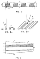
- Fig. 1 shows a resonance type wire grid polarizer, which can be used as a polarization beam splitter, according to this invention.
- Numeral 1 designates a metal grid, formed from a metal with a high reflectance, such as Au or Al, or a combination of these.
- the grids are designed to satisfy the following equations: 0.2 ⁇ h/d ⁇ 0.9 0.5 ⁇ b/d ⁇ 0.9 70° ⁇ s/d ⁇ 110°
- h is the thickness of the grid
- b is the width of the cross section, measured along a line passing 0.5h away from, and in parallel with, the base of the cross section
- s is the angle which is made by the base and a leg of the grid when a trapezoid is used to approximate the cross section of the grid
- "d” is the grid period
- "n 1 " is the refractive index of a substrate 2
- n 2 is the refractive index of a substance between grids
- n 3 is the refractive index of a substance over the grids.
- the angle of incidence on a wire grid polarizer is ⁇ when measured from the normal for the incidence surface of wire grid polarizer toward the direction V 1 of the wave vector of a grid and is ⁇ when measured from the normal toward the vertical direction V 2 to the wave vector of the grid.
- a laser direct lithography system is used to form a resist pattern of a 550-nm grid period "d" on a glass substrate with a refractive index n 1 of 1.50.
- Al is first deposited on the substrate to a thickness of about 2 nm, and then Au is deposited to a thickness of about 136 nm using an electron beam depositor to form grids composed of an Al layer (2 nm thick) and an Au layer (136 nm thick) by the lift-off method (the grids are hereinafter called Au grids).
- the cross section of a grid when observed under a scanning electron microscope, is found to be of a trapezoidal shape approximating to a rectangle wherein s ⁇ 80°, b/d ⁇ 0.6, and h/d ⁇ 0.25.
- the substrate to both sides of which matching oil 3 is applied, is sandwiched between wedge glass plates 4 (wedge angle: 1°) with a refractive index "n" of 1.50 to obtain a sample.
- the wedge glass plates 4 are used to accurately measure light reflected from a grid and transmitted light. Surfaces 5 and 6 may be covered with coating which reflects no light.
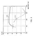
- Fig. 4 shows a curve (A) obtained by plotting S polarization reflectance Rs data measured in a wavelength range from 840 to 980 nm.
- the S polarization reflectance Rs has a minimum value of 1% or less at a wavelength of 950 nm.
- This S polarization resonance is expected to be the first to be observed for reflected light from an Au grid in a medium with a refractive index of 1.50.
- the P polarization reflectance is Rp ⁇ 60%, indicating that a resonance type wire grid polarizer is embodied for reflected light 950 nm in wavelength when the P polarization reflectance Rp ⁇ 60%, and Rp/Rs > 60.
- the curve (B) of Fig. 4 shows the results of measurements which are made in the same way as in the case of the curve (A) when a substrate is covered with the matching oil 3 having a refractive index "n" of 1.50 and the wedge glass plate 4, with Au grids of the same shape as in the first embodiment formed only on the back of a substrate (side on which grids are not formed in the first embodiment), and air on the face (side on which grids are formed in the first embodiment).
- the curve (B) shows that the S polarization reflectance Rs is almost constant, at about 70% and that resonance does not occur.
- the results show that, without nearly equalizing the refractive indexes n 1 , n 2 , and n 3 with each other (n 2 ⁇ n 3 ⁇ n 1 ), grids formed on the substrate 2 with a refractive index n 1 cannot be prompted to markedly resonate so that the S polarization reflectance has a minimum value of 2% or less, for example.
- the refractive indexes must satisfy the conditions
- the metal grids 1 made of Au show that, in activating resonance, it is essential for the cross section of the grids to be of a rectangular shape or a trapezoidal shape approximating to the rectangular shape. It is desired that the value of "s" be more than 70° and less that 110°.
- the angle of incidence ⁇ on a sample was about 10°.
- Fig. 5 shows that the ratio h/d must be adjusted to fabricate a resonance type wire grid polarizer which can be used for light with a specific wavelength.
- the resonance wavelength ⁇ res shifts to longer wavelengths, and thus the ratio b/d needs to be adjusted.
- the grid period "d" is selected so that ⁇ /2(n 1 ) ⁇ d ⁇ ⁇ /n 1 . This is because the grid period "d" is increased to facilitate grid fabrication. It is concluded by theoretical analysis that h/d ⁇ 0.9 in the case.
- the value of h/d is limited to the range from 0.2 to 0.9 exclusive (0.2 ⁇ h/d ⁇ 0.9).
- the minimum value of Rs was 2% or less for all data in Fig. 5, causing marked resonance to occur.
- the value of Rp was increased with increasing value of b/d. To satisfy a condition Rp > 60%, the value of b/d had to be larger than 0.5. Because of difficulty in grid fabrication, the value of b/d is less than 0.9, and thus the ratio b/d is limited so that it ranges from 0.5 to 0.9 exclusive (0.5 ⁇ b/d ⁇ 0.9).
- the S polarization transmittance Ts reached a peak at a wavelength a little longer than the resonance wavelength ⁇ res . That wavelength is represented by the symbol T s,res .
- the relationships between T s,res and metal materials for grids are shown in Fig. 6.
- the value of T s,res is low, at 50% for copper. It is also about 59% for an aluminum layer and about 57% for an Au layer underlaid with a titanium layer 5 nm thick. For the Au layer underlaid with the aluminum layer, the value of Ts,res was increased from 67% to 71% to 77% as the thickness of the aluminum layer is reduced from 5 nm to 2 nm to 1 nm.
- Au grids whose values of b/d and h/d are 0.65 and 0.45, respectively, are fabricated based on the results of experiments with the fourth embodiment.
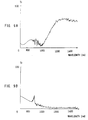
- the results of the determination of the dependence on wavelength of the S polarization transmittance Ts and the P polarization transmittance Tp are shown in Figs. 9A and 9B, respectively.
- a Ts value of approximately 70% and a Tp value of approximately 2% are obtained, resulting in a wire grid polarizer for transmitted light for which the value of Ts/Tp is approximately 35.
- the S polarization reflectance Rs was found to have a minimum value less than 2% at a wavelength of approximately 1300 nm, thus leading to marked resonance.
- the P polarization reflectance was about 70%.
- the fifth embodiment was found to offer polarization performance for reflected light for which Rp/Rs > 35, and a resonance type polarization beam splitter is ascertained to operate satisfactorily.
- angles of incidence ⁇ and ⁇ can properly be selected to adjust the resonance wavelength ⁇ res of a sample over a considerably wide range.
- increasing the angle of incidence ⁇ allows the resonance wavelength ⁇ res to shift to shorter wavelengths.
- setting the angle of incidence ⁇ larger allows a longer grid period in favor of wire grid polarizer fabrication when the wavelength of light to be used is determined.
- a matching oil with an refractive index "n" of 1.46 is applied to the grids, and they are sandwiched between wedge quartz substrates to obtain a sample.
- Fig. 12 shows the results of measurements of the dependence on wavelength of the S polarization reflectance Rs by use of the sample. The angle of incidence ⁇ was approximately 3°.
- the S polarization reflectance Rs had a minimum value of 1% or less near a wavelength of 840 nm. This and the results obtained from the sixth embodiment have shown that resonance is found to occur not only at specific wavelengths more than 1000 nm but at those around 800 nm.
- a resonance type wire grid polarizer is embodied for satisfactory reflected light.
- the S polarization reflectance Rs had a minimum value of 1% or less. Since aluminum has a high reflectance at short wavelengths of the order of 400 nm, setting the grid period "d" to approximately 400 nm / (1.44n 1 ) allows resonance to be utilized even at a wavelength of 400 nm.
- a resist pattern is first formed using a laser direct lithography system or an electron beam direct lithography system, then an Au coating or an Al coating is deposited on the pattern using an electron beam depositor, and finally, the resist and metal thereon are removed by immersing the resist in resist stripper, that is, by the "lift-off method.”
- Other methods can be used instead of the lift-off method.
- a metal coating is first deposited on the entire surface of a substrate by the evaporation method or by the spattering method, then a resist pattern is formed on the substrate, and finally, reactive ion etching (RIE) or Ar ion trimming is done to form metal grids.
- RIE reactive ion etching
- Mask exposure using an ultraviolet source, such as an excimer laser, and the two-light beam interference method are effective in forming a resist pattern.
Landscapes
- Physics & Mathematics (AREA)
- General Physics & Mathematics (AREA)
- Optics & Photonics (AREA)
- Polarising Elements (AREA)
Applications Claiming Priority (2)
| Application Number | Priority Date | Filing Date | Title |
|---|---|---|---|
| JP6340382A JPH08184711A (ja) | 1994-12-29 | 1994-12-29 | 偏光光学素子 |
| JP340382/94 | 1994-12-29 |
Publications (1)
| Publication Number | Publication Date |
|---|---|
| EP0721116A1 true EP0721116A1 (fr) | 1996-07-10 |
Family
ID=18336419
Family Applications (1)
| Application Number | Title | Priority Date | Filing Date |
|---|---|---|---|
| EP95402957A Withdrawn EP0721116A1 (fr) | 1994-12-29 | 1995-12-28 | Elément optique de polarisation |
Country Status (6)
| Country | Link |
|---|---|
| US (1) | US5748368A (fr) |
| EP (1) | EP0721116A1 (fr) |
| JP (1) | JPH08184711A (fr) |
| KR (1) | KR100390162B1 (fr) |
| CN (1) | CN1106581C (fr) |
| SG (1) | SG45132A1 (fr) |
Cited By (5)
| Publication number | Priority date | Publication date | Assignee | Title |
|---|---|---|---|---|
| WO2003032029A1 (fr) * | 2001-10-09 | 2003-04-17 | Koninklijke Philips Electronics N.V. | Dispositifs optiques |
| WO2003054619A3 (fr) * | 2001-12-21 | 2004-06-17 | Koninkl Philips Electronics Nv | Enceinte hermetique pour un polariseur a grille metallique et sous-ensemble pour systeme d'affichage |
| EP1390811A4 (fr) * | 2001-05-21 | 2009-03-18 | Moxtek Inc | Systeme de projection d'image a diviseur de faisceau polarisant |
| EP2228671A1 (fr) * | 2009-03-11 | 2010-09-15 | Giesecke & Devrient GmbH | Elément de sécurité |
| ITBO20090502A1 (it) * | 2009-07-30 | 2011-01-31 | Michele Giocondo | Filtro polarizzatore lineare con particolare efficienza di polarizzazione |
Families Citing this family (65)
| Publication number | Priority date | Publication date | Assignee | Title |
|---|---|---|---|---|
| US6208463B1 (en) * | 1998-05-14 | 2001-03-27 | Moxtek | Polarizer apparatus for producing a generally polarized beam of light |
| US6108131A (en) | 1998-05-14 | 2000-08-22 | Moxtek | Polarizer apparatus for producing a generally polarized beam of light |
| US6081376A (en) * | 1998-07-16 | 2000-06-27 | Moxtek | Reflective optical polarizer device with controlled light distribution and liquid crystal display incorporating the same |
| US6288840B1 (en) | 1999-06-22 | 2001-09-11 | Moxtek | Imbedded wire grid polarizer for the visible spectrum |
| US6122103A (en) * | 1999-06-22 | 2000-09-19 | Moxtech | Broadband wire grid polarizer for the visible spectrum |
| US6666556B2 (en) | 1999-07-28 | 2003-12-23 | Moxtek, Inc | Image projection system with a polarizing beam splitter |
| US6234634B1 (en) | 1999-07-28 | 2001-05-22 | Moxtek | Image projection system with a polarizing beam splitter |
| US7306338B2 (en) * | 1999-07-28 | 2007-12-11 | Moxtek, Inc | Image projection system with a polarizing beam splitter |
| US6243199B1 (en) * | 1999-09-07 | 2001-06-05 | Moxtek | Broad band wire grid polarizing beam splitter for use in the visible wavelength region |
| US6391528B1 (en) | 2000-04-03 | 2002-05-21 | 3M Innovative Properties Company | Methods of making wire grid optical elements by preferential deposition of material on a substrate |
| WO2002025325A1 (fr) * | 2000-09-20 | 2002-03-28 | Namiki Seimitsu Houseki Kabushiki Kaisha | Element polarisant, isolateur optique, module a diode laser et procede de production d'un element polarisant |
| JP2002090543A (ja) * | 2000-09-20 | 2002-03-27 | Namiki Precision Jewel Co Ltd | 偏光機能素子,光アイソレータ素子並びに光アイソレータ及びレーザダイオードモジュール |
| US6542307B2 (en) | 2000-10-20 | 2003-04-01 | Three-Five Systems, Inc. | Compact near-eye illumination system |
| US6563648B2 (en) | 2000-10-20 | 2003-05-13 | Three-Five Systems, Inc. | Compact wide field of view imaging system |
| US6532111B2 (en) | 2001-03-05 | 2003-03-11 | Eastman Kodak Company | Wire grid polarizer |
| US6585378B2 (en) | 2001-03-20 | 2003-07-01 | Eastman Kodak Company | Digital cinema projector |
| US7375887B2 (en) | 2001-03-27 | 2008-05-20 | Moxtek, Inc. | Method and apparatus for correcting a visible light beam using a wire-grid polarizer |
| RU2219570C2 (ru) * | 2001-08-31 | 2003-12-20 | Институт проблем лазерных и информационных технологий | Фазосдвигающий отражательный элемент |
| US6714350B2 (en) | 2001-10-15 | 2004-03-30 | Eastman Kodak Company | Double sided wire grid polarizer |
| US7061561B2 (en) * | 2002-01-07 | 2006-06-13 | Moxtek, Inc. | System for creating a patterned polarization compensator |
| US6909473B2 (en) * | 2002-01-07 | 2005-06-21 | Eastman Kodak Company | Display apparatus and method |
| US6785050B2 (en) * | 2002-05-09 | 2004-08-31 | Moxtek, Inc. | Corrosion resistant wire-grid polarizer and method of fabrication |
| US7131737B2 (en) * | 2002-06-05 | 2006-11-07 | Moxtek, Inc. | Housing for mounting a beamsplitter and a spatial light modulator with an output optical path |
| US6805445B2 (en) | 2002-06-05 | 2004-10-19 | Eastman Kodak Company | Projection display using a wire grid polarization beamsplitter with compensator |
| US6665119B1 (en) * | 2002-10-15 | 2003-12-16 | Eastman Kodak Company | Wire grid polarizer |
| US7113335B2 (en) * | 2002-12-30 | 2006-09-26 | Sales Tasso R | Grid polarizer with suppressed reflectivity |
| JP2005148416A (ja) * | 2003-11-14 | 2005-06-09 | Seizo Miyata | 偏光光学素子及びその連続的製造方法、並びに該偏光光学素子を使用した反射光学素子 |
| JP2005172844A (ja) * | 2003-12-05 | 2005-06-30 | Enplas Corp | ワイヤグリッド偏光子 |
| CN1316265C (zh) * | 2003-12-16 | 2007-05-16 | 财团法人工业技术研究院 | 具有双金属层光栅的偏光组件及其制造方法 |
| JP2005242080A (ja) * | 2004-02-27 | 2005-09-08 | Victor Co Of Japan Ltd | ワイヤグリッドポラライザ |
| US7304719B2 (en) * | 2004-03-31 | 2007-12-04 | Asml Holding N.V. | Patterned grid element polarizer |
| US7670758B2 (en) * | 2004-04-15 | 2010-03-02 | Api Nanofabrication And Research Corporation | Optical films and methods of making the same |
| US20050275944A1 (en) | 2004-06-11 | 2005-12-15 | Wang Jian J | Optical films and methods of making the same |
| US20060001969A1 (en) * | 2004-07-02 | 2006-01-05 | Nanoopto Corporation | Gratings, related optical devices and systems, and methods of making such gratings |
| US7414784B2 (en) * | 2004-09-23 | 2008-08-19 | Rohm And Haas Denmark Finance A/S | Low fill factor wire grid polarizer and method of use |
| US7630133B2 (en) | 2004-12-06 | 2009-12-08 | Moxtek, Inc. | Inorganic, dielectric, grid polarizer and non-zero order diffraction grating |
| US20080055719A1 (en) * | 2006-08-31 | 2008-03-06 | Perkins Raymond T | Inorganic, Dielectric Grid Polarizer |
| US7570424B2 (en) * | 2004-12-06 | 2009-08-04 | Moxtek, Inc. | Multilayer wire-grid polarizer |
| US7800823B2 (en) | 2004-12-06 | 2010-09-21 | Moxtek, Inc. | Polarization device to polarize and further control light |
| US7961393B2 (en) | 2004-12-06 | 2011-06-14 | Moxtek, Inc. | Selectively absorptive wire-grid polarizer |
| US7619816B2 (en) * | 2004-12-15 | 2009-11-17 | Api Nanofabrication And Research Corp. | Structures for polarization and beam control |
| US20060127830A1 (en) * | 2004-12-15 | 2006-06-15 | Xuegong Deng | Structures for polarization and beam control |
| US20070165308A1 (en) * | 2005-12-15 | 2007-07-19 | Jian Wang | Optical retarders and methods of making the same |
| US20070139771A1 (en) * | 2005-12-15 | 2007-06-21 | Jian Wang | Optical retarders and methods of making the same |
| US20070217008A1 (en) * | 2006-03-17 | 2007-09-20 | Wang Jian J | Polarizer films and methods of making the same |
| US8755113B2 (en) | 2006-08-31 | 2014-06-17 | Moxtek, Inc. | Durable, inorganic, absorptive, ultra-violet, grid polarizer |
| KR20080075753A (ko) * | 2007-02-13 | 2008-08-19 | 삼성전자주식회사 | 와이어 그리드 편광자 및 그 제조 방법 |
| US7789515B2 (en) | 2007-05-17 | 2010-09-07 | Moxtek, Inc. | Projection device with a folded optical path and wire-grid polarizer |
| JP2009031537A (ja) * | 2007-07-27 | 2009-02-12 | Seiko Epson Corp | 光学素子およびその製造方法、液晶装置、ならびに電子機器 |
| JP5349793B2 (ja) * | 2007-12-10 | 2013-11-20 | キヤノン株式会社 | 光学素子およびその製造方法 |
| CN101738668B (zh) | 2008-11-19 | 2011-12-07 | 上海丽恒光微电子科技有限公司 | 偏振立方体及其制造方法 |
| JP2010197764A (ja) * | 2009-02-26 | 2010-09-09 | Ricoh Co Ltd | 偏光制御素子及びそれを使用した画像表示装置 |
| US8248696B2 (en) | 2009-06-25 | 2012-08-21 | Moxtek, Inc. | Nano fractal diffuser |
| US8913321B2 (en) | 2010-09-21 | 2014-12-16 | Moxtek, Inc. | Fine pitch grid polarizer |
| US8611007B2 (en) | 2010-09-21 | 2013-12-17 | Moxtek, Inc. | Fine pitch wire grid polarizer |
| KR101282138B1 (ko) * | 2011-02-14 | 2013-07-04 | 삼성전자주식회사 | 디스플레이패널 및 이를 포함하는 디스플레이장치 |
| JP5762086B2 (ja) * | 2011-03-31 | 2015-08-12 | キヤノン株式会社 | 偏光分離素子および画像投射装置 |
| US8552439B2 (en) * | 2011-04-07 | 2013-10-08 | Himax Display, Inc. | Light-emitting diode package |
| US8873144B2 (en) | 2011-05-17 | 2014-10-28 | Moxtek, Inc. | Wire grid polarizer with multiple functionality sections |
| US8913320B2 (en) | 2011-05-17 | 2014-12-16 | Moxtek, Inc. | Wire grid polarizer with bordered sections |
| CN102323677B (zh) * | 2011-09-29 | 2013-06-19 | 上海丽恒光微电子科技有限公司 | 偏振分光器件及其形成方法 |
| US8922890B2 (en) * | 2012-03-21 | 2014-12-30 | Moxtek, Inc. | Polarizer edge rib modification |
| US9354374B2 (en) | 2013-10-24 | 2016-05-31 | Moxtek, Inc. | Polarizer with wire pair over rib |
| JP6534114B2 (ja) * | 2014-02-12 | 2019-06-26 | 国立大学法人三重大学 | 光学装置の製造方法及び光学装置 |
| CN111308596A (zh) * | 2020-02-13 | 2020-06-19 | 中国科学院福建物质结构研究所 | 一种偏振分束光栅及其制作方法 |
Citations (6)
| Publication number | Priority date | Publication date | Assignee | Title |
|---|---|---|---|---|
| US2224214A (en) * | 1937-12-28 | 1940-12-10 | Polaroid Corp | Light polarizing body |
| US3436143A (en) * | 1965-11-30 | 1969-04-01 | Bell Telephone Labor Inc | Grid type magic tee |
| US3536373A (en) * | 1964-03-09 | 1970-10-27 | Polaroid Corp | Light polarizer |
| US4009933A (en) * | 1975-05-07 | 1977-03-01 | Rca Corporation | Polarization-selective laser mirror |
| US4289381A (en) * | 1979-07-02 | 1981-09-15 | Hughes Aircraft Company | High selectivity thin film polarizer |
| EP0416157A1 (fr) * | 1989-09-07 | 1991-03-13 | Max-Planck-Gesellschaft zur Förderung der Wissenschaften e.V. | Polariseur |
Family Cites Families (1)
| Publication number | Priority date | Publication date | Assignee | Title |
|---|---|---|---|---|
| JPH03289692A (ja) * | 1990-04-06 | 1991-12-19 | Matsushita Electric Ind Co Ltd | 空間光変調素子及びこれを用いたホログラム画像情報記録装置 |
-
1994
- 1994-12-29 JP JP6340382A patent/JPH08184711A/ja active Pending
-
1995
- 1995-12-21 US US08/576,686 patent/US5748368A/en not_active Expired - Fee Related
- 1995-12-22 SG SG1995002284A patent/SG45132A1/en unknown
- 1995-12-27 KR KR1019950058358A patent/KR100390162B1/ko not_active Expired - Fee Related
- 1995-12-28 EP EP95402957A patent/EP0721116A1/fr not_active Withdrawn
- 1995-12-29 CN CN95113172A patent/CN1106581C/zh not_active Expired - Fee Related
Patent Citations (6)
| Publication number | Priority date | Publication date | Assignee | Title |
|---|---|---|---|---|
| US2224214A (en) * | 1937-12-28 | 1940-12-10 | Polaroid Corp | Light polarizing body |
| US3536373A (en) * | 1964-03-09 | 1970-10-27 | Polaroid Corp | Light polarizer |
| US3436143A (en) * | 1965-11-30 | 1969-04-01 | Bell Telephone Labor Inc | Grid type magic tee |
| US4009933A (en) * | 1975-05-07 | 1977-03-01 | Rca Corporation | Polarization-selective laser mirror |
| US4289381A (en) * | 1979-07-02 | 1981-09-15 | Hughes Aircraft Company | High selectivity thin film polarizer |
| EP0416157A1 (fr) * | 1989-09-07 | 1991-03-13 | Max-Planck-Gesellschaft zur Förderung der Wissenschaften e.V. | Polariseur |
Non-Patent Citations (2)
| Title |
|---|
| LOCHBIHLER ET AL: "Characterization of Highly Conducting Wire Gratings using an Electromagnetic Theory of Diffraction", OPTICS COMMUNICATIONS, vol. 100, 1 July 1993 (1993-07-01), AMSTERDAM NL, pages 231 - 238, XP002001890 * |
| LOCHBIHLER H ET AL: "CHARACTERIZATION OF X-RAY TRANSMISSION GRATINGS", APPLIED OPTICS, vol. 31, no. 7, 1 March 1992 (1992-03-01), pages 964 - 971, XP000248796 * |
Cited By (5)
| Publication number | Priority date | Publication date | Assignee | Title |
|---|---|---|---|---|
| EP1390811A4 (fr) * | 2001-05-21 | 2009-03-18 | Moxtek Inc | Systeme de projection d'image a diviseur de faisceau polarisant |
| WO2003032029A1 (fr) * | 2001-10-09 | 2003-04-17 | Koninklijke Philips Electronics N.V. | Dispositifs optiques |
| WO2003054619A3 (fr) * | 2001-12-21 | 2004-06-17 | Koninkl Philips Electronics Nv | Enceinte hermetique pour un polariseur a grille metallique et sous-ensemble pour systeme d'affichage |
| EP2228671A1 (fr) * | 2009-03-11 | 2010-09-15 | Giesecke & Devrient GmbH | Elément de sécurité |
| ITBO20090502A1 (it) * | 2009-07-30 | 2011-01-31 | Michele Giocondo | Filtro polarizzatore lineare con particolare efficienza di polarizzazione |
Also Published As
| Publication number | Publication date |
|---|---|
| KR960025436A (ko) | 1996-07-20 |
| CN1157931A (zh) | 1997-08-27 |
| CN1106581C (zh) | 2003-04-23 |
| KR100390162B1 (ko) | 2003-09-22 |
| US5748368A (en) | 1998-05-05 |
| JPH08184711A (ja) | 1996-07-16 |
| SG45132A1 (en) | 1998-01-16 |
Similar Documents
| Publication | Publication Date | Title |
|---|---|---|
| EP0721116A1 (fr) | Elément optique de polarisation | |
| EP1411377B1 (fr) | Polariseur à grille métallique | |
| EP1212644B1 (fr) | Separateur de faisceau polarisant ameliore a grille metallique pour la region visible du spectre optique | |
| JP4800437B2 (ja) | 可視スペクトル用の広帯域ワイヤグリッド偏光子 | |
| Leyva et al. | Narrow bandwidth volume holographic optical filter operating at the Kr transition at 1547.82 nm | |
| US5007708A (en) | Technique for producing antireflection grating surfaces on dielectrics, semiconductors and metals | |
| EP0349309B1 (fr) | Polariseur de type de réseau de diffraction biréfringent | |
| US20040125449A1 (en) | Grid polarizer with suppressed reflectivity | |
| JP2004280050A5 (fr) | ||
| JP2006138842A (ja) | 金属光フィルタを用いた検出装置及び検出方法 | |
| US4501470A (en) | Christiansen-Bragg optical filter | |
| US5608577A (en) | Optical mirror and optical device using the same | |
| JP5137084B2 (ja) | 偏光子、その製造方法及び光モジュール | |
| JP3488776B2 (ja) | テーパ導波路およびそれを用いた光導波路素子 | |
| US7020373B2 (en) | Antireflective coating structure for photonic crystal and method for forming antireflective coating structure | |
| JPH09178943A (ja) | 偏光光学素子 | |
| JP2000137109A (ja) | 回折格子を利用した反射防止デバイス | |
| EP0484626B1 (fr) | Séparateur de faisceaux polarisant | |
| Kim et al. | Multilayer thin-film design as far-ultraviolet polarizers | |
| JPH07107561B2 (ja) | 多層光学素子 | |
| JP3874301B2 (ja) | 偏光光学素子 | |
| Pogossian et al. | Neutron low-index thin-film waveguides with antiresonant high-reflection layers | |
| Dansas et al. | Fast modelling of light beam diffraction by multilayer structures including a grating coupler | |
| CA2393924A1 (fr) | Dispositif de polarisation optique et dispositif de polarisation d'un laser | |
| Vertiy et al. | Application of multilayer structures at millimeter wavelengths |
Legal Events
| Date | Code | Title | Description |
|---|---|---|---|
| PUAI | Public reference made under article 153(3) epc to a published international application that has entered the european phase |
Free format text: ORIGINAL CODE: 0009012 |
|
| AK | Designated contracting states |
Kind code of ref document: A1 Designated state(s): DE FR GB |
|
| 17P | Request for examination filed |
Effective date: 19961220 |
|
| 17Q | First examination report despatched |
Effective date: 20001004 |
|
| STAA | Information on the status of an ep patent application or granted ep patent |
Free format text: STATUS: THE APPLICATION IS DEEMED TO BE WITHDRAWN |
|
| 18D | Application deemed to be withdrawn |
Effective date: 20010418 |