EP0721135B1 - Optische Wellenleitervorrichtung - Google Patents
Optische Wellenleitervorrichtung Download PDFInfo
- Publication number
- EP0721135B1 EP0721135B1 EP96103061A EP96103061A EP0721135B1 EP 0721135 B1 EP0721135 B1 EP 0721135B1 EP 96103061 A EP96103061 A EP 96103061A EP 96103061 A EP96103061 A EP 96103061A EP 0721135 B1 EP0721135 B1 EP 0721135B1
- Authority
- EP
- European Patent Office
- Prior art keywords
- optical waveguide
- conductive layer
- light
- optical
- control electrodes
- Prior art date
- Legal status (The legal status is an assumption and is not a legal conclusion. Google has not performed a legal analysis and makes no representation as to the accuracy of the status listed.)
- Expired - Lifetime
Links
- 230000003287 optical effect Effects 0.000 title claims description 180
- 239000013078 crystal Substances 0.000 claims description 49
- 239000000758 substrate Substances 0.000 claims description 34
- 230000000694 effects Effects 0.000 claims description 20
- 230000010287 polarization Effects 0.000 claims description 6
- 230000002269 spontaneous effect Effects 0.000 claims description 5
- 230000008878 coupling Effects 0.000 claims description 4
- 238000010168 coupling process Methods 0.000 claims description 4
- 238000005859 coupling reaction Methods 0.000 claims description 4
- 238000003780 insertion Methods 0.000 description 27
- 230000037431 insertion Effects 0.000 description 27
- 230000007613 environmental effect Effects 0.000 description 15
- 230000000052 comparative effect Effects 0.000 description 14
- 239000013307 optical fiber Substances 0.000 description 14
- 238000000034 method Methods 0.000 description 11
- 229910003327 LiNbO3 Inorganic materials 0.000 description 9
- RTAQQCXQSZGOHL-UHFFFAOYSA-N Titanium Chemical compound [Ti] RTAQQCXQSZGOHL-UHFFFAOYSA-N 0.000 description 9
- 238000010276 construction Methods 0.000 description 9
- 238000012538 light obscuration Methods 0.000 description 9
- 239000010936 titanium Substances 0.000 description 9
- 229910052719 titanium Inorganic materials 0.000 description 9
- 239000000835 fiber Substances 0.000 description 7
- 229910052751 metal Inorganic materials 0.000 description 7
- 239000002184 metal Substances 0.000 description 7
- 230000008033 biological extinction Effects 0.000 description 5
- 229910012463 LiTaO3 Inorganic materials 0.000 description 4
- 230000005684 electric field Effects 0.000 description 3
- 238000005259 measurement Methods 0.000 description 3
- 150000002739 metals Chemical class 0.000 description 3
- 239000004065 semiconductor Substances 0.000 description 3
- 238000005507 spraying Methods 0.000 description 3
- 238000007740 vapor deposition Methods 0.000 description 3
- OKTJSMMVPCPJKN-UHFFFAOYSA-N Carbon Chemical compound [C] OKTJSMMVPCPJKN-UHFFFAOYSA-N 0.000 description 2
- QPLDLSVMHZLSFG-UHFFFAOYSA-N Copper oxide Chemical compound [Cu]=O QPLDLSVMHZLSFG-UHFFFAOYSA-N 0.000 description 2
- 239000005751 Copper oxide Substances 0.000 description 2
- XLOMVQKBTHCTTD-UHFFFAOYSA-N Zinc monoxide Chemical compound [Zn]=O XLOMVQKBTHCTTD-UHFFFAOYSA-N 0.000 description 2
- AZWHFTKIBIQKCA-UHFFFAOYSA-N [Sn+2]=O.[O-2].[In+3] Chemical compound [Sn+2]=O.[O-2].[In+3] AZWHFTKIBIQKCA-UHFFFAOYSA-N 0.000 description 2
- 230000001174 ascending effect Effects 0.000 description 2
- 239000006229 carbon black Substances 0.000 description 2
- 229910000431 copper oxide Inorganic materials 0.000 description 2
- 238000002474 experimental method Methods 0.000 description 2
- 238000010438 heat treatment Methods 0.000 description 2
- 229910003437 indium oxide Inorganic materials 0.000 description 2
- PJXISJQVUVHSOJ-UHFFFAOYSA-N indium(iii) oxide Chemical compound [O-2].[O-2].[O-2].[In+3].[In+3] PJXISJQVUVHSOJ-UHFFFAOYSA-N 0.000 description 2
- 238000000206 photolithography Methods 0.000 description 2
- 238000007650 screen-printing Methods 0.000 description 2
- RYGMFSIKBFXOCR-UHFFFAOYSA-N Copper Chemical compound [Cu] RYGMFSIKBFXOCR-UHFFFAOYSA-N 0.000 description 1
- 239000007836 KH2PO4 Substances 0.000 description 1
- LFVGISIMTYGQHF-UHFFFAOYSA-N ammonium dihydrogen phosphate Chemical compound [NH4+].OP(O)([O-])=O LFVGISIMTYGQHF-UHFFFAOYSA-N 0.000 description 1
- 229910002113 barium titanate Inorganic materials 0.000 description 1
- 230000005540 biological transmission Effects 0.000 description 1
- 230000015572 biosynthetic process Effects 0.000 description 1
- 229910052799 carbon Inorganic materials 0.000 description 1
- 239000011203 carbon fibre reinforced carbon Substances 0.000 description 1
- 238000004891 communication Methods 0.000 description 1
- 229910052802 copper Inorganic materials 0.000 description 1
- 239000010949 copper Substances 0.000 description 1
- 238000010304 firing Methods 0.000 description 1
- 229910002804 graphite Inorganic materials 0.000 description 1
- 239000010439 graphite Substances 0.000 description 1
- 125000004435 hydrogen atom Chemical group [H]* 0.000 description 1
- 238000011835 investigation Methods 0.000 description 1
- 229910052744 lithium Inorganic materials 0.000 description 1
- 150000002641 lithium Chemical group 0.000 description 1
- 238000004519 manufacturing process Methods 0.000 description 1
- 229910000402 monopotassium phosphate Inorganic materials 0.000 description 1
- 230000001590 oxidative effect Effects 0.000 description 1
- 238000009832 plasma treatment Methods 0.000 description 1
- GNSKLFRGEWLPPA-UHFFFAOYSA-M potassium dihydrogen phosphate Chemical compound [K+].OP(O)([O-])=O GNSKLFRGEWLPPA-UHFFFAOYSA-M 0.000 description 1
- 230000008569 process Effects 0.000 description 1
- 230000004044 response Effects 0.000 description 1
- 230000008054 signal transmission Effects 0.000 description 1
Images


Classifications
-
- G—PHYSICS
- G02—OPTICS
- G02F—OPTICAL DEVICES OR ARRANGEMENTS FOR THE CONTROL OF LIGHT BY MODIFICATION OF THE OPTICAL PROPERTIES OF THE MEDIA OF THE ELEMENTS INVOLVED THEREIN; NON-LINEAR OPTICS; FREQUENCY-CHANGING OF LIGHT; OPTICAL LOGIC ELEMENTS; OPTICAL ANALOGUE/DIGITAL CONVERTERS
- G02F1/00—Devices or arrangements for the control of the intensity, colour, phase, polarisation or direction of light arriving from an independent light source, e.g. switching, gating or modulating; Non-linear optics
- G02F1/01—Devices or arrangements for the control of the intensity, colour, phase, polarisation or direction of light arriving from an independent light source, e.g. switching, gating or modulating; Non-linear optics for the control of the intensity, phase, polarisation or colour
- G02F1/03—Devices or arrangements for the control of the intensity, colour, phase, polarisation or direction of light arriving from an independent light source, e.g. switching, gating or modulating; Non-linear optics for the control of the intensity, phase, polarisation or colour based on ceramics or electro-optical crystals, e.g. exhibiting Pockels effect or Kerr effect
- G02F1/035—Devices or arrangements for the control of the intensity, colour, phase, polarisation or direction of light arriving from an independent light source, e.g. switching, gating or modulating; Non-linear optics for the control of the intensity, phase, polarisation or colour based on ceramics or electro-optical crystals, e.g. exhibiting Pockels effect or Kerr effect in an optical waveguide structure
-
- G—PHYSICS
- G02—OPTICS
- G02F—OPTICAL DEVICES OR ARRANGEMENTS FOR THE CONTROL OF LIGHT BY MODIFICATION OF THE OPTICAL PROPERTIES OF THE MEDIA OF THE ELEMENTS INVOLVED THEREIN; NON-LINEAR OPTICS; FREQUENCY-CHANGING OF LIGHT; OPTICAL LOGIC ELEMENTS; OPTICAL ANALOGUE/DIGITAL CONVERTERS
- G02F1/00—Devices or arrangements for the control of the intensity, colour, phase, polarisation or direction of light arriving from an independent light source, e.g. switching, gating or modulating; Non-linear optics
- G02F1/01—Devices or arrangements for the control of the intensity, colour, phase, polarisation or direction of light arriving from an independent light source, e.g. switching, gating or modulating; Non-linear optics for the control of the intensity, phase, polarisation or colour
- G02F1/03—Devices or arrangements for the control of the intensity, colour, phase, polarisation or direction of light arriving from an independent light source, e.g. switching, gating or modulating; Non-linear optics for the control of the intensity, phase, polarisation or colour based on ceramics or electro-optical crystals, e.g. exhibiting Pockels effect or Kerr effect
- G02F1/05—Devices or arrangements for the control of the intensity, colour, phase, polarisation or direction of light arriving from an independent light source, e.g. switching, gating or modulating; Non-linear optics for the control of the intensity, phase, polarisation or colour based on ceramics or electro-optical crystals, e.g. exhibiting Pockels effect or Kerr effect with ferro-electric properties
-
- G—PHYSICS
- G02—OPTICS
- G02F—OPTICAL DEVICES OR ARRANGEMENTS FOR THE CONTROL OF LIGHT BY MODIFICATION OF THE OPTICAL PROPERTIES OF THE MEDIA OF THE ELEMENTS INVOLVED THEREIN; NON-LINEAR OPTICS; FREQUENCY-CHANGING OF LIGHT; OPTICAL LOGIC ELEMENTS; OPTICAL ANALOGUE/DIGITAL CONVERTERS
- G02F1/00—Devices or arrangements for the control of the intensity, colour, phase, polarisation or direction of light arriving from an independent light source, e.g. switching, gating or modulating; Non-linear optics
- G02F1/29—Devices or arrangements for the control of the intensity, colour, phase, polarisation or direction of light arriving from an independent light source, e.g. switching, gating or modulating; Non-linear optics for the control of the position or the direction of light beams, i.e. deflection
- G02F1/31—Digital deflection, i.e. optical switching
- G02F1/313—Digital deflection, i.e. optical switching in an optical waveguide structure
- G02F1/3132—Digital deflection, i.e. optical switching in an optical waveguide structure of directional coupler type
-
- G—PHYSICS
- G02—OPTICS
- G02F—OPTICAL DEVICES OR ARRANGEMENTS FOR THE CONTROL OF LIGHT BY MODIFICATION OF THE OPTICAL PROPERTIES OF THE MEDIA OF THE ELEMENTS INVOLVED THEREIN; NON-LINEAR OPTICS; FREQUENCY-CHANGING OF LIGHT; OPTICAL LOGIC ELEMENTS; OPTICAL ANALOGUE/DIGITAL CONVERTERS
- G02F1/00—Devices or arrangements for the control of the intensity, colour, phase, polarisation or direction of light arriving from an independent light source, e.g. switching, gating or modulating; Non-linear optics
- G02F1/29—Devices or arrangements for the control of the intensity, colour, phase, polarisation or direction of light arriving from an independent light source, e.g. switching, gating or modulating; Non-linear optics for the control of the position or the direction of light beams, i.e. deflection
- G02F1/31—Digital deflection, i.e. optical switching
- G02F1/313—Digital deflection, i.e. optical switching in an optical waveguide structure
- G02F1/3137—Digital deflection, i.e. optical switching in an optical waveguide structure with intersecting or branching waveguides, e.g. X-switches and Y-junctions
-
- G—PHYSICS
- G02—OPTICS
- G02F—OPTICAL DEVICES OR ARRANGEMENTS FOR THE CONTROL OF LIGHT BY MODIFICATION OF THE OPTICAL PROPERTIES OF THE MEDIA OF THE ELEMENTS INVOLVED THEREIN; NON-LINEAR OPTICS; FREQUENCY-CHANGING OF LIGHT; OPTICAL LOGIC ELEMENTS; OPTICAL ANALOGUE/DIGITAL CONVERTERS
- G02F2203/00—Function characteristic
- G02F2203/21—Thermal instability, i.e. DC drift, of an optical modulator; Arrangements or methods for the reduction thereof
Definitions
- the present invention relates to optical waveguide devices comprising an optical waveguide substrate made of ferroelectric crystals.
- optical waveguide devices In the fields of optical measurement systems, optical communication systems, etc., it is known to manufacture optical waveguide devices by forming three dimensional optical waveguides in various electro-optics crystals.
- optical waveguide devices optical branch devices, optical modulation devices, optical polarization devices, optical switches, multiplexer, and so on are known.
- the optical waveguide devices have such advantages as small size, good stability, low necessary power and high speed signal transmission.
- a light impinging upon one end of the optical waveguide is divided by a ratio of 50:50% at a branch portion of the optical waveguide.
- One of the divided light is phase-modulated by applying a predetermined voltage.
- Phase differences due to Sagnac effects which are generated by a rotation of the objected optical systems, are detected by the optical waveguide device. The thus obtained phase difference is introduced into a formula showing the relation between a rotation angular rate of the optical system and a phase difference to obtain a rotation angular rate.
- the inventors further investigated an intensity modulator of Mach-Zehnder type formed by arranging an optical waveguide of Mach-Zehnder type in the substrate.
- this intensity modulator a light impinging upon the intensity modulator is divided. Respective divided lights are phase-modulated by applying a voltage thereto. Then, the modulated lights are interfered to vary the intensity.
- the inventors faced to the problems mentioned below.
- the modulator for fiber optic gyroscope it is necessary to set the dividing ratio substantially equal to 50:50.
- an admission range of the dividing ratio is very narrow. This is because, in the case that the dividing ratio is out of 50:50, the detected rotation angular rate is largely varied even if the rotation rate of the optical system is not varied.
- the dividing ratio is temporarily varied from 50:50 to 40:60, the obtained rotation angular rate is varied about 20%. Therefore, in the modulator for fiber optic gyroscope, it is required to set the dividing ratio within 48:52 ⁇ 50:50. Moreover, the optical waveguide device is principally required to act stably along a wide temperature range. However, if an environmental temperature of the optical waveguide device was varied, the dividing ratio at the branch portion of the optical waveguide was temporarily varied largely. As a result, the dividing ratio of 50:50 was varied to 30:70, especially to substantially 100:0. Moreover, in addition to the light dividing ratio variation, a light insertion loss of the optical waveguide device occurred.
- the Mach-Zehnder intensity modulator if the light dividing ratio was varied, an extinction ratio is varied largely, and the light insertion loss of the overall optical waveguide device is temporarily increased at the same time.
- JP-60-257325 discloses an optical waveguide device including branch arms diverging from a junction point, and extending to a modulating region.
- a rectangular guard electrode surrounds the branch point and modulating region. The guard electrode is said to reduce temperature dependence and a pyroelectric effect.
- It is an object of the invention to provide an optical waveguide device comprising an optical waveguide substrate made of ferroelectric crystals, and an optical waveguide formed in a principal plane of the optical waveguide substrate, at least one functional portion for a light dividing or a light coupling being formed in the light waveguide, in which, a light insertion loss, a light dividing ratio and an extinction ratio are not varied, even if an environmental temperature of the optical waveguide device is varied.
- the invention provides an optical waveguide device according to claim 1.
- the inventors investigated the reason for varying the light insertion loss, the light dividing ratio and the extinction ratio at the functional portion of the light waveguide.
- the pyroelectrical effects function to generate a large number of charges in a crystal plane of the optical waveguide substrate in a spontaneous electric polarization direction, and electric fields due to the charges were largely interfered to a light transmission at the functional portions.
- the first conductive layer was formed in one region defined from a boundary between the first crystal plane and the major plane to the functional portion, and the second conductive layer was formed in the other region defined from a boundary between the second crystal plane and the major plane to the functional portion. Then, the first conductive layer and the second conductive layer were electrically conducted. As a result, we found that variations of the light insertion loss, the light dividing ratio and the extinction ratio were extraordinarily reduced.
- the conductive layers are arranged in the regions defined from the functional portions of the optical waveguide to respective crystal planes in which the charges are generated due to the pyroelectrical effects. Therefore, if the charges are generated in respective crystal planes, lines of electric force become coarse near the conductive layers, and thus a potential gradient between the conductive layers becomes small accordingly. Therefore, we think that the pyroelectrical effects to the functional portions become small. Moreover, since the first conductive layer and the second conductive layer are electrically conducted, potentials of respective conductive layers arranged to both side portions of the functional portion become almost equal, and thus the pyroelectrical effects can be reduced.
- No conductive layers are preferably formed to both of the first crystal plane and the second crystal plane in which the charges are directly generated, and the charges instantaneously generated in the crystal planes are not neutralized. However, even if the charges generated in the crystal planes are not directly neutralized, it is possible to prevent the affections instantaneously applied to the functional portions at which a light is divided.
- a buffer layer is formed on a surface of an optical waveguide, and an antistatic layer is formed on the buffer layer. Moreover, a control electrode is formed on the antistatic layer.
- the charges generated by the pyroelectrical effects are deviated ununiformly in the crystal surface due to an effect of the control electrode.
- the antistatic layer only prevents the charge ununiformity, and does not function to neutralize instantaneously the charges generated by the pyroelectrical effects.
- the optical waveguide has a linear shape, and thus there is no problem about a variation of the light dividing ratio.
- a pair of ferroelectric substrates are connected via a conductive member in such a manner that respective spontaneous electric polarization are reversed with each other so as to reduce the pyroelectrical effects.
- the charges generated in connection surfaces of the ferro-electric substrates can be neutralized, but the charges generated in the other surfaces than the connection surfaces cannot be neutralized. Therefore, electric fields remain in the ferroelectric substrates, and thus the pyroelectrical effects cannot be eliminated.
- the optical waveguide has a linear shape, and thus there is no problem about a variation of the light dividing ratio.
- the electrical conduction between the first conductive layer and the second conductive layer is preferably performed in one of the following methods.
- control electrodes are preferably arranged at outer portions and inner portions of respective divided optical waveguides, and control voltages can be applied to respective divided optical waveguides by the control electrodes, the first conductive layer and the second conductive layer can be electrically conducted to the control electrodes of the outer portions respectively.
- the first conductive layer and the second conductive layer can be electrically isolated from the control electrodes of the outer portions respectively.
- the pyroelectrical effects can be preferably eliminated.
- third conductive layers are formed on regions between a plurality of divided optical waveguides, and the third conductive layers are electrically conducted to at least one of the first conductive layer and the second conductive layer. In this case, even in an inner region of the functional portions, the pyroelectrical effects can be preferably eliminated.
- the control electrodes are arranged at outer portions and inner portions of respective divided optical waveguides, and control voltages can be applied to respective divided optical waveguides by the control electrodes, it is preferred to isolate the third conductive layers from the control electrodes of the inner portions of respective divided optical waveguides. If the third conductive layers are electrically conducted to the control electrodes of the inner portion, potentials of respective conductive layers are affected by potential variations of the control electrodes of the inner portions. Especially, in the case that the first conductive layer and the second conductive layer are electrically conducted to the control electrodes of the outer portions, it is necessary to electrically isolate the third conductive layer from the control electrodes of the inner portions.
- ferroelectric crystals it is preferred to use one or more ferroelectric crystals selected from the group consisting of LiNbO 3 , LiTaO 3 , Li(Nb x , Ta 1-x ), BaTiO 3 , ZnO, NH 4 H 2 PO 4 , KH 2 PO 4 and KTiOPO 4 . Moreover, it is more preferred to use one or more ferroelectric crystal selected from LiNbO 3 , LiTaO 3 and Li(Nb x , Ta 1-x ).
- optical waveguide it is preferred to use (1) optical waveguide formed by thermally diffusing titanium or copper into ferroelectric crystal, or (2) optical waveguide formed by proton-exchange process in which lithium atom in LiNbO 3 crystal, LiTaO 3 crystal or Li(Nb x , Ta 1-x ) O 3 crystal is exchanged by hydrogen atom.
- the present invention can be applied to optical waveguides of ridge type, optical waveguides of dielectric load type, optical waveguide of metal load type, etc.
- At least one functional portions for dividing or coupling lights is arranged in the optical waveguide.
- a shape of the optical waveguide may be planar or may be curvature.
- the functional portions may be so-called Y-branch portion or directional couplers.
- the Y-branch portion is formed by coupling one row of the optical waveguide and two rows of the optical waveguides, and functions to divide and/or couple lights.
- the directional coupler is formed by arranging adjacent optical waveguides very closely and functions to shift a guided light from on optical waveguide to the other optical waveguide. Therefore, a guided light can be divided by the directional coupler at any light dividing ratios. Moreover, the directional coupler can be used together with the Y-branch.
- the optical waveguide devices according to the invention can be used for active devices and passive devices.
- the passive devices use is made of beam splitters, star couplers having a waveguide of cascade type consisting of a plurality of Y-branch portions, and so on.
- the active devices use is made of light intensity modulators, phase modulators, optical switching devices, acoustic-optics devices, logic devices for optical computer (AND element, OR element), multiple modulators having such a construction that optical modulation electrodes are arranged to the star coupler, and so on.
- the optical waveguide devices according to the invention can be preferably used for the above-mentioned aims.
- the Mach-Zehnder light intensity modulator there is a problem such that the extinction ration is varied.
- the present invention can preferably eliminate such a problem.
- the optical waveguide devices for dividing lights such as the beam splitters, the optical switching devices, the logic devices, and so on, they output erroneous values if the divided lights are varied. Therefore, the second aspect of the invention can be preferably applied for such devices.
- ON-OFF states are detected from the divided lights transmitted through two rows of optical waveguides. Therefore, if the divided lights are varied over the threshold level, the ON state and the OFF state are exchanged, and thus it is not possible to use them.
- a plurality of Y-branch portions are arranged to make the cascade construction. Therefore, if the light dividing ratio of respective Y-branch portions is varied out of the predetermined value, these variations are multiplied from input to output. Therefore, even if the variation of the light dividing ratio at one Y-branch portion is for example 5%, the multiplied variations become extraordinarily large value.
- the invention can be preferably applied to star couplers and multiple modulators.
- a resistivity R of the conducted portion should be set in such a manner that electric fields applied to the optical waveguide portion is always below 10 V/cm under thinkable temperature variation rate.
- V QR/d
- Q the charges (coulomb) generated during a unit time, which depends on the environmental temperatures
- R is a resistivity ( ⁇ ) of the conducted portion
- d is a distance between the first crystal plane and the second crystal plane.
- the resistivity R of the conducted portion should be designed to satisfy R ⁇ 10d/Q.
- the resistivities of both of the first conductive layer and the second conductive layer may be set below 100 ⁇ /cm 2 .
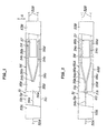
- Fig. 1 is a plane view showing one embodiment of the invention.
- an optical waveguide device 51 is formed by an X-cut plate made of LiNbO 3 , LiTaO 3 or Li(Nb x , Ta 1-x ).
- a three dimensional optical waveguide 54 is formed in a major plane 51a of the optical waveguide device 51.
- the optical waveguide 54 comprises a linear portion 54a in a light input side, a Y-branch portion 54b and a pair of linear portions 54c.
- An optical fiber support substrate 53A is connected to alight input side of the optical waveguide substrate 51 to support an optical fiber 52A.
- the optical fiber 52A is optically coupled with the linear portion 54a.
- An optical fiber support substrate 53B is connected to a light output side of the optical waveguide substrate 51 to support a pair of optical fibers 52B.
- the optical fibers 52B are optically coupled with the linear portions 54c respectively.
- a spontaneous electric polarization direction of the optical waveguide substrate 1 made of ferroelectric crystals is a direction shown by an arrow A and is substantially perpendicular to a light proceeding direction. It is sufficient to cross this spontaneous electric polarization direction to the light proceeding direction by a predetermined angle, but it is preferred to set the cross angle at 90°.
- the optical waveguide substrate 51 has a first crystal plane 51b and a second crystal plane 51c. Positive charges and negative charges are generated respectively in the first crystal plane 51b and the second crystal plane 51c due to the pyroelectrical effects.
- a first conductive layer 56a is formed in one region 55A extending from a boundary between the first crystal plane 51b and the major plane 51a to the Y-branch portion 54b, and a second conductive layer 56c is formed in the other region 55B extending from a boundary between the second crystal plane 51b and the major plane 51a to the Y-branch portion 54b.
- the first conductive layer 56a and the second conductive layer 56c are integrated to construct an integrated conductive layer 56.
- Respective conductive layers 56a, 56c has a rectangular shape. Outer sides of respective conductive layers 56a, 56c are linear along a boundary between the major plane 51a and respective crystal planes. Inner sides of respective conductive layers 56a, 56c are substantially along a shape of the optical waveguide. Respective conductive layers 56a, 56c are integrated by a connection portion 56e, and the connection portion 56e is arranged on the optical waveguide 54.
- respective conductive layers 56a, 56c are arranged symmetrically with respect to a horizontal line.
- Thin control electrodes 56b, 56d are extended parallelly from respective conductive layers 56a, 56c.
- Respective linear portions 54c is arranged between inner control electrode 57 and respective control electrodes 56b or 56d.
- Figs. 2 and 3 are plane views respectively showing another embodiment according to the invention.
- Figs. 2 and 3 portions similar to those of Fig. 1 are denoted by the same numerals, and the explanations thereof are omitted here.
- a pair of conductive layers 66A and 66B are arranged outside of the optical waveguide 54 and are arranged symmetrically with respect to a horizontal line.
- the conductive layer 66A comprises a first conductive layer 66a and a control electrode 66b.
- the conductive layer 66b comprises a second conductive layer 66c and a control electrode 66d.
- Respective conductive layers 66a, 66c has a rectangular shape. Outer sides of respective conductive layers 66a, 66c are linear along a boundary between the major plane 51a and respective crystal planes. Inner sides of respective conductive layers 66a, 66c are substantially along a shape of the optical waveguide.
- Thin control electrodes 66b, 66d are extended parallelly from respective conductive layers 66a, 66c.
- Respective linear portions 54c is arranged between the inner control electrode 57 and respective control electrodes 56b or 56d.
- first conductive layer 66a and the second conductive layer 66c are electrically conducted by a connection member 60.
- connection member 60 use is made of a conductive stripe, a conductive wire and so on.
- a conductive layer 76 is isolated from a pair of control electrodes 58. Therefore, the conductive layer 76 has no voltage apply function.
- Respective linear portions 54c are arranged respectively between the control electrode 57 and one of the control electrodes 58.
- the conductive layer 76 comprises a first conductive layer 76a, a second conductive layer 26b and a connection portion 76c.
- Respective conductive layers 76a, 76b has a rectangular shape. Outer sides of respective conductive layers 76a, 76b are linear along a boundary between the major plane 51a and respective crystal planes. Inner sides of respective conductive layers 76a, 76b are substantially along a shape of the optical waveguide.
- the connection portion 76c is arranged on the optical waveguide 54.
- the first conductive layer and the second conductive layer have a rectangular shape, and the inner sides of the conductive layers are along a shape of the optical waveguide. Therefore, a space between respective conductive layers and the optical waveguide and a space between the major plane 51a and an edge portion can be small, and thus the pyroelectrical effects for the Y-branch portions can be minimized.
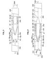
- FIGs. 4 and 5 are plane views respectively showing one embodiment of Mach-Zehnder light intensity modulator according to the invention.
- an optical waveguide 64 comprises a linear portion 64a in a light input side, a Y-branch portion 64b, a pair of linear portion 64c, a Y-branch portion 64d and a linear portion 64e in a light output side.
- the optical fiber 52A is coupled to the linear portion 64a, and the optical fiber 52B is coupled to the linear portion 64e.
- the conductive layer 56 is formed only in the side of the Y-branch portion 64b.
- Respective conductive layers 56a, 56c has a rectangular shape. Outer sides of the conductive layers 56a, 56c are linear along a boundary between the major plane 51a and respective crystal planes. Inner sides of the conductive layers 56a, 56c are substantially along a shape of the optical waveguide.
- Respective conductive layers 56a, 56c are integrated at the connection portion 56e, and the connection portion 56e is arranged on the optical waveguide 14.
- respective conductive layers 56a, 56c are arranged symmetrically with respect to a horizontal line.
- Thin control electrodes 56b, 56d are extended parallelly from respective conductive layers 56a, 56c.
- a control electrode 67 arranged between a pair of the linear portions 64c comprises a rectangular portion 67a and a triangular portion 67b.
- Respective linear portions 64c is arranged between the rectangular portion 67a and the control electrodes 56b or 56d.
- the triangular portion 67b is extended toward the Y-branch portion 64b.
- a shape of the conductive layer 86 will be explained.
- almost all region 55A is covered with a first conductive layer 86a and almost all region 55B is covered with a second conductive layer 86c.
- almost all region 55C extended from a boundary between the first conductive layer 51b and the major plane 51a to the Y-branch portion 64d is covered with a first conductive layer 86f.
- almost all region 55D extended from a boundary between the second crystal plane 51c and the major plane 51a to the Y-branch portion 64d is covered with a second conductive layer 86g.
- Respective conductive layers 86a, 86c, 86f and 86g has a rectangular shape. Outer sides of respective conductive layers 86a, 86c, 86f and 86g are linear along a boundary between the major plane 51a and respective crystal planes. Inner sides of these conductive layer are linear along a shape of the optical waveguide.
- the conductive layers 86a and 86c are integrated at a connection portion 86e, and the connection portion 86e is arranged on the optical waveguide 64.
- the conductive layers 86f and 86g are integrated at a connection portion 86h, and the connection portion 86h is arranged on the optical waveguide 64. In Fig.
- the conductive layers 86a and 86c and the conductive layers 86f and 86g are respectively arranged symmetrically with respect to a horizontal line.
- the conductive layers 86a and 86f and the conductive layers 86c and 86g are respectively connected by thin control electrodes 36a and 36d.
- the control electrode 77 comprises a rectangular portion 77a and triangular portions 77b and 77c.
- the linear portions 64c are respectively arranged between the rectangular portion 77a and the control electrode 86b or between the rectangular portion 77a and the control electrode 86d.
- the triangular portion 77b is extended toward the Y-branch portion 64b, and the triangular portion 77c is extended toward the Y-branch portion 64d.
- optical waveguide devices according to the examples of the invention and according to the comparative examples were manufactured. Then, properties as the phase modulator for use in fiber optics gyroscope were measured.
- optical waveguide devices As for the optical waveguide devices according to the examples of the invention, use was made of the optical waveguide device having the construction shown in Fig. 1.
- the optical waveguide devices were manufactured in the following manner. At first, a disk-shape wafer made of LiNbO 3 having X-cut plane was prepared. The wafer head a diameter of 3 inches and a thickness of 1 mm. A titanium thin layer having a width of 3 ⁇ m and a thickness of 500 angstrom was formed on the wafer by using the photolithography technic, and a titanium component was diffused into the LiNbO 3 wafer by effecting a heat treatment such as 1000°C ⁇ 6 hours to form the titanium diffused optical waveguide 54.
- conductive layer 56 and the control electrode 57 both made of metal layers, were respectively formed by a spraying method and so on. Gap distances between the electrode 57 and the control electrodes 56b or 56d were 10 ⁇ m, and a length of the electrode 57 was 15 mm. From this wafer, the optical waveguide substrates 51 for one chip were cut out.
- the optical fibers 52A and 52B were connected as shown in Fig. 1 to obtain specimens according to the invention.
- the optical waveguide devices having a construction shown in Fig. 6a according to the comparative example were manufactured in the same manner as mentioned above.
- the specimens according to the comparative examples have electrodes 58 in spite of the conductive layer 56.
- the optical waveguide devices according to the examples of the invention and according to the comparative examples were accommodated in the temperature adjusting apparatus shown in Fig. 13. Then, a light having a wavelength of 0.85 ⁇ m was introduced from a light source, and output lights transmitted through a pair of optical fibers 52B were measured by a pair of light amount measuring apparatuses. After that, a light insertion loss and a light dividing ratio were calculated from respective measured values.
- the environmental temperature of the optical waveguide devices were varied. That is to say, the environmental temperature was varied stepwise from 20°C to -40°C. In this case, a holding time at respective temperatures was about 45 minutes, and an ascending rate and a descending rate of temperature was 80°C/hour.
- Fig. 7 shows the results of the comparative example
- Fig. 8 shows the results of the example according to the invention.
- a region of the light insertion loss more 4dB and a region of the light dividing ratio more than 30:70 were cut out.
- both of the light insertion loss and the light dividing ratio were not varied as shown in Fig. 8.
- a variation of the light insertion loss was less than 0.4dB
- a variation of the light dividing ratio was in a range of 50:50 ⁇ 52:48.
- the optical waveguide devices according to the present invention and according to the comparative example were assembled in the fiber optics gyroscopes as modulators. Then, as shown in Figs. 7 and 8, the environmental temperature was varied. As a result, in the comparative example, the calculated rotation angular rate was varied by more than 20%, and sometimes it was not possible to measure the rotation angular rate.
- optical waveguide devices shown in Figs. 2 and 3 were manufactured in the same manner mentioned above. Then, the same experiment was performed with respect to respective optical waveguide devices. As a result, the same results as those shown in Fig. 8 were obtained.
- optical waveguide devices according to the examples of the invention and according to the comparative examples were manufactured. Then, properties of the Mack-Zehnder light intensity modulator were measured. As for the optical waveguide devices according to the examples of the invention, use was made of the optical waveguide devices having the constructions shown in Figs. 4 and 5.
- the optical waveguide devices were manufactured in the following manner. At first, a disk-shape wafer made of LiNbO 3 having X-cut plane was prepared. The wafer had a diameter of 3 inches and a thickness of 1 mm. A titanium thin layer having a width of 3 ⁇ m and a thickness of 500 angstrom was formed on the wafer by using the photolithography technic, and titanium component was diffused into the LiNbO 3 wafer by effecting a heat treatment such as 1000°C ⁇ 6 hours to form the titanium diffused optical waveguide 64.
- the conductive layers 56, 86 and the control electrodes 67, 77 both made of metal layers, were respectively formed by a spraying method and so on. Thicknesses of the conductive layers 56, 86 and the control electrodes 67, 77 were 2500 angstrom. From this wafer the optical waveguide substrates 51 for one chip were cut out.
- the optical fibers 52A and 52B were connected as shown in Figs. 4 and 5 to obtain specimens according to the invention.
- the optical waveguide devices having a construction shown in Fig. 6b according to the comparative example were manufactured in the same manner as mentioned above.
- the specimens according to the comparative example have electrodes 18 and 37 in spite of the conductive layers 56, 86 and the control electrodes 67, 77.
- the optical waveguide devices according to the examples of the invention and according to the comparative examples were accommodated in the temperature adjusting apparatus shown in Fig. 13. Then, a light having a wavelength of 0.85 ⁇ m was introduced from a light source, and output lights transmitted through a pair of optical fibers 52B were measured by a pair of light amount adjusting apparatuses. After that, a light insertion loss and a light extinction ratio in a temperature stable state (-20°C) were measured. Moreover, the light insertion loss and the light extinction ratio were measured when a temperature was varied at a rate of 80°C/hour.
- the light intensity in a temperature variable state was varied as shown in Fig. 10b.
- This light extinction ratio was 2dB.
- the light insertion loss in a temperature variable state was increased by 3dB as compared with that in a temperature stable state. In this manner, if the conductive layers 56a, 56c were arranged around the Y-branch portion 64b, the light extinction ratio in a temperature variable state can be extraordinarily improved.
- the light intensity in a temperature variable state was varied as shown in Fig. 10c.
- This light extinction ratio was 20dB.
- the light insertion loss in a temperature variable state was increased by only less than 0.1dB as compared with that in a temperature stable state. In this manner, if the conductive layers 86a, 86c, 86f, 86g were arranged around the Y-branch portions 64b and 64d, both of the light extinction ratio and the light insertion loss in a temperature variable state can be extraordinarily improved.
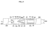
- Fig. 11 is a plan view showing another embodiment of the optical waveguide device according to the invention, which relates to the optical waveguide substrate having Y-branch portions shown in Figs. 1 to 3.
- a conductive layer 76 is isolated from a pair of the control electrodes 58, and does not function to apply a voltage.
- the linear portions 54c in a light output side are arranged respectively between the control electrode 57 and the control electrode 58.
- the integrated conductive layer 76 comprises a first conductive layer 76a, a second conductive layer 76b and a connection portion 76c.
- the conductive layers 76a, 76b have a rectangular shape.
- Outer sides of the conductive layers 76a, 76b are linear along a boundary between the major plane 51a and respective crystal planes. Inner sides of the conductive layers 76a, 76b are along a shape of the optical waveguide.
- the connection portion 76c is arranged on the optical waveguide 54.
- a third conductive layer 80 having a triangular shape is formed, and the third conductive layer 80 and the second conductive layer 76b are electrically conducted by means of the connection member 60.
- the third conductive layer 80 and the control electrode 57 are isolated.
- the optical waveguide device show in Fig. 11 was manufactured, and the same experiments as those of the example 1 were performed.
- the titanium diffused optical waveguide 54 was formed in the optical waveguide substrate 51 by using a titanium diffusing method.
- the conductive layers 76, 80 and the control electrodes 57, 58 both made of metal layers, were formed by a spraying method and so on. Thicknesses of the conductive layers 76, 80 and the control electrodes 57, 58 were 2500 angstrom. A gap distance between the control electrodes 57 and 58 was 10 ⁇ m, and a length of respective control electrodes was 15 mm. From this wafer, the optical waveguide substrates 51 for one chip were cut out. To both ends of the optical waveguide substrate 51, the optical fibers 52A, 52B are connected as shown in Fig. 11 to obtain the specimens.
- the thus obtained optical waveguide device shown in Fig. 11 was accommodated in the temperature adjusting apparatus. Then, a light having a wavelength of 0.85 ⁇ m was introduced from the light source, and output lights transmitted through a pair of optical fibers 2B were measured by a pair of light amount measuring apparatuses. After that, a light insertion loss and a light dividing ratio were calculated from respective measured values.
- the environmental temperature of the optical waveguide devices were varied. That is to say, the environmental temperature was varied stepwise from 80°C to -40°C. In this case, a holding time at respective temperature was about 45 minutes, and an ascending rate and a descending rate of temperature was 80°C/hour.
- both of the light insertion loss and the light dividing ratio were not varied. That is to say, in a wide temperature range of -40°C ⁇ +80°C, a variation of the light insertion loss was 0.3dB and a variation of the light dividing ratio was in a range of 48:52 ⁇ 49.8:50.2. Especially, in a temperature range of -40°C ⁇ +20°C, a variation of the light insertion loss was less than 0.2dB, and a variation of the light dividing ratio was in a range of 48:52 ⁇ 49:51.
- the optical waveguide device showing no variations of the light insertion loss, the light dividing ratio and the light extinction ratio at functional portions in the optical waveguide even if the environmental temperature is varied.
Landscapes
- Physics & Mathematics (AREA)
- Nonlinear Science (AREA)
- Chemical & Material Sciences (AREA)
- Engineering & Computer Science (AREA)
- Ceramic Engineering (AREA)
- Crystallography & Structural Chemistry (AREA)
- General Physics & Mathematics (AREA)
- Optics & Photonics (AREA)
- Optical Integrated Circuits (AREA)
Claims (8)
- Optische Wellenleiter-Vorrichtung, umfassend ein optisches Wellenleiter-Substrat (51), einen optischen Wellenleiter (54), der in einer Hauptebene (51a) des optischen Wellenleiter-Substrats (51) ausgebildet ist, wobei der optische Wellenleiter einen linearen Abschnitt (54a) umfasst, und zumindest einen Funktionsabschnitt (54b) zum Teilen oder Koppeln von Lichtstrahlen, umfassend Verzweigungsarme, die von einem Verbindungspunkt abzweigen, wobei das Wellenleiter-Substrat (51) aus einem ferroelektrischen Kristall besteht, dessen spontane elektrische Polarisationsrichtung quer zur Normalen auf die Hauptebene (51a) und zum linearen Abschnitt (54a) verläuft, eine erste im optischen Wellenleiter-Substrat ausgebildete Kristallebene (51b), in der Ladungen einer Polarität aufgrund des pyroelektrischen Effekts erzeugt werden, eine zweite im optischen Wellenleiter-Substrat ausgebildete Kristallebene (51c), in der Ladungen der anderen Polarität aufgrund des pyroelektrischen Effekts erzeugt werden, eine erste leitende Schicht (56a), die in einem Bereich (55A) ausgebildet ist, der von einer Grenze zwischen der ersten Kristallebene (51b) und der Hauptebene (51a) bis zum Funktionsabschnitt (54b) definiert ist, sowie eine zweite leitende Schicht (56c), die in einem anderen Bereich (55B) ausgebildet ist, der von einer Grenze zwischen der zweiten Kristallebene (51b) und der Hauptebene (51a) bis zum Funktionsabschnitt (54b) definiert ist, worin die erste leitende Schicht (56a) und die zweite leitende Schicht (56c) elektrisch miteinander verbunden sind,
dadurch gekennzeichnet, dass die Innenränder der jeweiligen leitenden Schichten (56a, 56c) entlang der Verzweigungsarme des optischen Wellenleiters (54) angeordnet sind. - Optische Wellenleiter-Vorrichtung nach Anspruch 1, worin die erste leitende Schicht (56a) und die zweite leitende Schicht (56c) über Drähte (60) oder Leiterstreifen elektrisch miteinander verbunden sind.
- Optische Wellenleiter-Vorrichtung nach Anspruch 1, worin die erste leitende Schicht (56a) und die zweite leitende Schicht (56c) einstückig ausgebildet sind.
- Optische Wellenleiter-Vorrichtung nach einem der Ansprüche 1 bis 3, worin Steuerelektroden (56b, 56d, 57) auf dem optischen Wellenleiter-Substrat (51) an einem äußeren Abschnitt und einem inneren Abschnitt des Funktionsabschnitts des optischen Wellenleiters (54) ausgebildet sind, um an den optischen Wellenleiter (54) eine Spannung anzulegen, und die erste leitende Schicht (56a) und die zweite leitende Schicht (56c) mit den jeweiligen Steuerelektroden (56b, 56d) an einem äußeren Abschnitt elektrisch verbunden sind.
- Optische Wellenleiter-Vorrichtung nach einem der Ansprüche 1 bis 3, worin Steuerelektroden (58, 57) auf dem optischen Wellenleiter-Substrat (51) an einem äußeren Abschnitt und einem inneren Abschnitt des Funktionsabschnitts des optischen Wellenleiters (54) ausgebildet sind, um an den optischen Wellenleiter (54) eine Spannung anzulegen, und die erste leitende Schicht (76a) und die zweite leitende Schicht (76b) von den Steuerelektroden (58) am äußeren Abschnitt elektrisch isoliert sind.
- Optische Wellenleiter-Vorrichtung nach einem der Ansprüche 1 bis 5, worin eine dritte leitende Schicht (80) auf dem optischen Wellenleiter-Substrat (51) in einem Bereich zwischen getrennten optischen Wellenleitern (54c) ausgebildet ist und die dritte leitende Schicht (80) mit zumindest einer von erster leitender Schicht (76a) und zweiter leitender Schicht (76b) elektrisch verbunden ist.
- Optische Wellenleiter-Vorrichtung nach Anspruch 6, worin Steuerelektroden (58, 57) auf dem optischen Wellenleiter-Substrat an einem äußeren Abschnitt und einem inneren Abschnitt des Funktionsabschnitts der optischen Wellenleiter ausgebildet sind, um eine Spannung an den optischen Wellenleiter (54) anzulegen, und die dritte leitende Schicht (80) von der Steuerelektrode (57) am inneren Abschnitt elektrisch isoliert ist.
- Optische Wellenleiter-Vorrichtung nach einem der Ansprüche 1 bis 7, worin der Funktionsabschnitt (54b) ein Y-Verzweigungsabschnitt oder ein Richtungskoppler ist.
Applications Claiming Priority (13)
| Application Number | Priority Date | Filing Date | Title |
|---|---|---|---|
| JP21160693 | 1993-08-26 | ||
| JP21160693 | 1993-08-26 | ||
| JP211606/93 | 1993-08-26 | ||
| JP221038/93 | 1993-09-06 | ||
| JP22103893 | 1993-09-06 | ||
| JP22103893 | 1993-09-06 | ||
| JP180102/94 | 1994-08-01 | ||
| JP18010294 | 1994-08-01 | ||
| JP18010294A JPH07120631A (ja) | 1993-09-06 | 1994-08-01 | 光導波路型部品 |
| JP181527/94 | 1994-08-02 | ||
| JP18152794A JPH07113992A (ja) | 1993-08-26 | 1994-08-02 | 光導波路型部品 |
| JP18152794 | 1994-08-02 | ||
| EP94306331A EP0640861B1 (de) | 1993-08-26 | 1994-08-26 | Optische Wellenleiter-Vorrichtung |
Related Parent Applications (2)
| Application Number | Title | Priority Date | Filing Date |
|---|---|---|---|
| EP94306331A Division EP0640861B1 (de) | 1993-08-26 | 1994-08-26 | Optische Wellenleiter-Vorrichtung |
| EP94306331.3 Division | 1994-08-26 |
Publications (2)
| Publication Number | Publication Date |
|---|---|
| EP0721135A1 EP0721135A1 (de) | 1996-07-10 |
| EP0721135B1 true EP0721135B1 (de) | 2001-11-07 |
Family
ID=27474919
Family Applications (2)
| Application Number | Title | Priority Date | Filing Date |
|---|---|---|---|
| EP96103061A Expired - Lifetime EP0721135B1 (de) | 1993-08-26 | 1994-08-26 | Optische Wellenleitervorrichtung |
| EP94306331A Expired - Lifetime EP0640861B1 (de) | 1993-08-26 | 1994-08-26 | Optische Wellenleiter-Vorrichtung |
Family Applications After (1)
| Application Number | Title | Priority Date | Filing Date |
|---|---|---|---|
| EP94306331A Expired - Lifetime EP0640861B1 (de) | 1993-08-26 | 1994-08-26 | Optische Wellenleiter-Vorrichtung |
Country Status (3)
| Country | Link |
|---|---|
| US (1) | US5621839A (de) |
| EP (2) | EP0721135B1 (de) |
| DE (2) | DE69421477T2 (de) |
Families Citing this family (12)
| Publication number | Priority date | Publication date | Assignee | Title |
|---|---|---|---|---|
| JP2873203B2 (ja) * | 1996-06-14 | 1999-03-24 | 住友大阪セメント株式会社 | 導波路型光デバイス |
| US6044184A (en) * | 1998-03-31 | 2000-03-28 | Litton Systems Inc. | Integrated optics chip with reduced thermal errors due to pyroelectric effects |
| DE60021996T2 (de) | 1999-12-15 | 2006-06-08 | Ngk Insulators, Ltd., Nagoya | Optischer Wanderwellenmodulator und Verfahren zu seiner Herstellung |
| JP2002023123A (ja) * | 2000-07-11 | 2002-01-23 | Fujitsu Ltd | 非主要光を導波する光導波路を備える光回路 |
| US20030031400A1 (en) * | 2001-06-28 | 2003-02-13 | Valerio Pruneri | Integrated optical waveguide device |
| JP2003043272A (ja) * | 2001-07-27 | 2003-02-13 | Nec Corp | 導波路型光デバイス |
| JP2004281742A (ja) * | 2003-03-17 | 2004-10-07 | Japan Science & Technology Agency | 半導体素子、半導体センサーおよび半導体記憶素子 |
| JP2005331885A (ja) * | 2004-05-21 | 2005-12-02 | Fujitsu Ltd | 音響光学デバイスおよび音響光学デバイスの製造方法 |
| JP4789460B2 (ja) * | 2004-12-22 | 2011-10-12 | 株式会社アドバンテスト | 光スイッチ及び光試験装置 |
| US20090225392A1 (en) * | 2008-03-10 | 2009-09-10 | Depriest Christopher Michael | Optical Modulator and Method of Providing the Same |
| KR101845514B1 (ko) * | 2010-12-17 | 2018-04-04 | 삼성전자주식회사 | 소형 광 변조기 및 이를 포함하는 광 송신기 |
| JP6911329B2 (ja) * | 2016-11-09 | 2021-07-28 | 富士通オプティカルコンポーネンツ株式会社 | 光変調器および光モジュール |
Family Cites Families (6)
| Publication number | Priority date | Publication date | Assignee | Title |
|---|---|---|---|---|
| JPS60257325A (ja) * | 1984-06-05 | 1985-12-19 | Yokogawa Hokushin Electric Corp | 光電圧センサ |
| JPH02257108A (ja) * | 1989-03-30 | 1990-10-17 | Nec Corp | 光導波路デバイス |
| JPH0727131B2 (ja) * | 1990-08-24 | 1995-03-29 | 日本航空電子工業株式会社 | 光導波路型変調器 |
| US5185823A (en) * | 1990-12-13 | 1993-02-09 | Japan Aviation Electronics Industry Limited | Waveguide type optical device |
| JPH0588125A (ja) * | 1991-09-26 | 1993-04-09 | Sumitomo Cement Co Ltd | 光導波路及びその作製方法 |
| CA2083219C (en) * | 1991-11-19 | 1999-01-05 | Hiroshi Nishimoto | Optical transmitter having optical modulator |
-
1994
- 1994-08-24 US US08/294,915 patent/US5621839A/en not_active Expired - Lifetime
- 1994-08-26 DE DE69421477T patent/DE69421477T2/de not_active Expired - Fee Related
- 1994-08-26 EP EP96103061A patent/EP0721135B1/de not_active Expired - Lifetime
- 1994-08-26 DE DE69429009T patent/DE69429009T2/de not_active Expired - Fee Related
- 1994-08-26 EP EP94306331A patent/EP0640861B1/de not_active Expired - Lifetime
Also Published As
| Publication number | Publication date |
|---|---|
| US5621839A (en) | 1997-04-15 |
| EP0640861A3 (de) | 1995-09-20 |
| DE69421477T2 (de) | 2000-05-04 |
| DE69421477D1 (de) | 1999-12-09 |
| DE69429009D1 (de) | 2001-12-13 |
| EP0640861B1 (de) | 1999-11-03 |
| EP0721135A1 (de) | 1996-07-10 |
| EP0640861A2 (de) | 1995-03-01 |
| DE69429009T2 (de) | 2002-06-06 |
Similar Documents
| Publication | Publication Date | Title |
|---|---|---|
| US7088875B2 (en) | Optical modulator | |
| US5862276A (en) | Planar microphotonic circuits | |
| US7447389B2 (en) | Optical modulator | |
| US5263102A (en) | Polarization-independent optical switches/modulators | |
| US4262993A (en) | Electrooptically balanced alternating Δβ switch | |
| EP0721135B1 (de) | Optische Wellenleitervorrichtung | |
| JP2002350796A (ja) | マッハ−ツェンダ電子−光学変調器 | |
| US20050123228A1 (en) | Optical deflector and optical switch | |
| US20210223657A1 (en) | Active photonic networks on integrated lithium niobate platforms | |
| JP2806425B2 (ja) | 導波型光デバイス | |
| JPH0667130A (ja) | 光制御素子 | |
| JP3043614B2 (ja) | 導波路型光デバイス | |
| JPH07120631A (ja) | 光導波路型部品 | |
| JP2000028979A (ja) | 偏波無依存光制御素子 | |
| Schmidt | Integrated optics switches and modulators | |
| JPH037910A (ja) | 導波路型光回路素子 | |
| US20040047533A1 (en) | Device for contolling polarisation in an optical connection | |
| US5050947A (en) | Optical waveguide control device employing directional coupler on substrate | |
| JP2877125B2 (ja) | 導波型光アレスター | |
| Okayama et al. | Directional coupler switch with reduced voltage-length product | |
| JPH05303022A (ja) | 単一モード光学装置 | |
| JPH0425524B2 (de) | ||
| JP3139712B2 (ja) | 光制御デバイス | |
| JPH02114243A (ja) | 光制御デバイス及びその製造方法 | |
| Pedersen et al. | A high-speed 4* 4 Ti: LiNbO 3 integrated optic switch at 1.5 μm |
Legal Events
| Date | Code | Title | Description |
|---|---|---|---|
| PUAI | Public reference made under article 153(3) epc to a published international application that has entered the european phase |
Free format text: ORIGINAL CODE: 0009012 |
|
| 17P | Request for examination filed |
Effective date: 19960315 |
|
| AC | Divisional application: reference to earlier application |
Ref document number: 640861 Country of ref document: EP |
|
| AK | Designated contracting states |
Kind code of ref document: A1 Designated state(s): DE FR GB IT |
|
| 17Q | First examination report despatched |
Effective date: 19981202 |
|
| GRAG | Despatch of communication of intention to grant |
Free format text: ORIGINAL CODE: EPIDOS AGRA |
|
| GRAG | Despatch of communication of intention to grant |
Free format text: ORIGINAL CODE: EPIDOS AGRA |
|
| GRAH | Despatch of communication of intention to grant a patent |
Free format text: ORIGINAL CODE: EPIDOS IGRA |
|
| GRAH | Despatch of communication of intention to grant a patent |
Free format text: ORIGINAL CODE: EPIDOS IGRA |
|
| GRAH | Despatch of communication of intention to grant a patent |
Free format text: ORIGINAL CODE: EPIDOS IGRA |
|
| GRAA | (expected) grant |
Free format text: ORIGINAL CODE: 0009210 |
|
| AC | Divisional application: reference to earlier application |
Ref document number: 640861 Country of ref document: EP |
|
| AK | Designated contracting states |
Kind code of ref document: B1 Designated state(s): DE FR GB IT |
|
| REF | Corresponds to: |
Ref document number: 69429009 Country of ref document: DE Date of ref document: 20011213 |
|
| REG | Reference to a national code |
Ref country code: GB Ref legal event code: IF02 |
|
| PGFP | Annual fee paid to national office [announced via postgrant information from national office to epo] |
Ref country code: GB Payment date: 20020816 Year of fee payment: 9 |
|
| PGFP | Annual fee paid to national office [announced via postgrant information from national office to epo] |
Ref country code: FR Payment date: 20020821 Year of fee payment: 9 |
|
| PGFP | Annual fee paid to national office [announced via postgrant information from national office to epo] |
Ref country code: DE Payment date: 20020824 Year of fee payment: 9 |
|
| PLBE | No opposition filed within time limit |
Free format text: ORIGINAL CODE: 0009261 |
|
| STAA | Information on the status of an ep patent application or granted ep patent |
Free format text: STATUS: NO OPPOSITION FILED WITHIN TIME LIMIT |
|
| 26N | No opposition filed | ||
| PG25 | Lapsed in a contracting state [announced via postgrant information from national office to epo] |
Ref country code: GB Free format text: LAPSE BECAUSE OF NON-PAYMENT OF DUE FEES Effective date: 20030826 |
|
| PG25 | Lapsed in a contracting state [announced via postgrant information from national office to epo] |
Ref country code: DE Free format text: LAPSE BECAUSE OF NON-PAYMENT OF DUE FEES Effective date: 20040302 |
|
| GBPC | Gb: european patent ceased through non-payment of renewal fee | ||
| PG25 | Lapsed in a contracting state [announced via postgrant information from national office to epo] |
Ref country code: FR Free format text: LAPSE BECAUSE OF NON-PAYMENT OF DUE FEES Effective date: 20040430 |
|
| REG | Reference to a national code |
Ref country code: FR Ref legal event code: ST |
|
| PG25 | Lapsed in a contracting state [announced via postgrant information from national office to epo] |
Ref country code: IT Free format text: LAPSE BECAUSE OF NON-PAYMENT OF DUE FEES Effective date: 20050826 |