EP0723366A2 - Procédé d'estimation du mouvement et appareil pour calculer un vecteur de mouvement - Google Patents
Procédé d'estimation du mouvement et appareil pour calculer un vecteur de mouvement Download PDFInfo
- Publication number
- EP0723366A2 EP0723366A2 EP96300175A EP96300175A EP0723366A2 EP 0723366 A2 EP0723366 A2 EP 0723366A2 EP 96300175 A EP96300175 A EP 96300175A EP 96300175 A EP96300175 A EP 96300175A EP 0723366 A2 EP0723366 A2 EP 0723366A2
- Authority
- EP
- European Patent Office
- Prior art keywords
- data sets
- candidate blocks
- pel
- calculating
- blocks
- Prior art date
- Legal status (The legal status is an assumption and is not a legal conclusion. Google has not performed a legal analysis and makes no representation as to the accuracy of the status listed.)
- Withdrawn
Links
Images


Classifications
-
- H—ELECTRICITY
- H04—ELECTRIC COMMUNICATION TECHNIQUE
- H04N—PICTORIAL COMMUNICATION, e.g. TELEVISION
- H04N5/00—Details of television systems
- H04N5/14—Picture signal circuitry for video frequency region
- H04N5/144—Movement detection
- H04N5/145—Movement estimation
-
- G—PHYSICS
- G06—COMPUTING OR CALCULATING; COUNTING
- G06T—IMAGE DATA PROCESSING OR GENERATION, IN GENERAL
- G06T7/00—Image analysis
- G06T7/20—Analysis of motion
- G06T7/223—Analysis of motion using block-matching
- G06T7/231—Analysis of motion using block-matching using full search
-
- H—ELECTRICITY
- H04—ELECTRIC COMMUNICATION TECHNIQUE
- H04N—PICTORIAL COMMUNICATION, e.g. TELEVISION
- H04N19/00—Methods or arrangements for coding, decoding, compressing or decompressing digital video signals
- H04N19/42—Methods or arrangements for coding, decoding, compressing or decompressing digital video signals characterised by implementation details or hardware specially adapted for video compression or decompression, e.g. dedicated software implementation
- H04N19/43—Hardware specially adapted for motion estimation or compensation
-
- H—ELECTRICITY
- H04—ELECTRIC COMMUNICATION TECHNIQUE
- H04N—PICTORIAL COMMUNICATION, e.g. TELEVISION
- H04N19/00—Methods or arrangements for coding, decoding, compressing or decompressing digital video signals
- H04N19/50—Methods or arrangements for coding, decoding, compressing or decompressing digital video signals using predictive coding
- H04N19/503—Methods or arrangements for coding, decoding, compressing or decompressing digital video signals using predictive coding involving temporal prediction
- H04N19/51—Motion estimation or motion compensation
- H04N19/523—Motion estimation or motion compensation with sub-pixel accuracy
-
- G—PHYSICS
- G06—COMPUTING OR CALCULATING; COUNTING
- G06T—IMAGE DATA PROCESSING OR GENERATION, IN GENERAL
- G06T2200/00—Indexing scheme for image data processing or generation, in general
- G06T2200/28—Indexing scheme for image data processing or generation, in general involving image processing hardware
-
- G—PHYSICS
- G06—COMPUTING OR CALCULATING; COUNTING
- G06T—IMAGE DATA PROCESSING OR GENERATION, IN GENERAL
- G06T2207/00—Indexing scheme for image analysis or image enhancement
- G06T2207/10—Image acquisition modality
- G06T2207/10016—Video; Image sequence
Definitions
- the present invention relates to motion estimation method and apparatus for calculating a motion vector, and more particularly to method and apparatus for calculating a motion vector to estimate a current picture partially forming a video sequence on the basis of a reference picture partially forming the video sequence.
- multimedia In the recent years, information transmitting media such as news paper, TV and radio have been flooded with information relative to "multimedia” to which ardent attention is paid by all the world.
- multimedia is considered to be information presented in the combination of text, graphics, video, sound and the like. Since such information is generally handled by a computer, data representative of the video and sound as well as the text and graphics are required to be digitized. When data representative of a video sequence such as a motion picture are digitized, the amount of digitized data is extremely large in comparison with data indicative of sound, text or graphics. For this reason, the data of a motion picture to be handled by the computer are required to be compressed when the data is stored in a storage device or transmitted over a communication line.
- This method comprises a step of calculating a difference between pel data of each pel (picture element) of a current picture 12 and pel data of each pel of a reference picture 11 corresponding in position to each other, the current picture 12 and the reference picture 11 partially forming a motion picture.
- the reference picture 11 may be either of feature and past pictures with respect to the current picture 12 upon condition that data indicative of the reference picture 11 have been already encoded.
- the method further comprises steps of comparing the difference with a predetermined threshold value, and dividing the pel data of the reference picture 11 into two data groups consisting of a significant pel data group having differences each larger than the threshold value and an insignificant pel data group having differences each equal to or less than the threshold value.
- the significant pel data are considered to be useful data that are not allowed to be omitted when the current picture 12 is estimated on the basis of the reference picture 11.
- the insignificant pel data are considered to be unnecessary data that are allowed to be omitted when the current picture 12 is estimated on the basis of the reference picture 11.
- the difference data between two pels decrease fast as the significant pel data is fewer.
- the number of the significant pel is decreased by setting the threshold value large and as a consequence the compression efficiency can be further enhanced. If, however, the threshold value becomes extremely large, motion of the image looks to be jerky, or moving portion of the image looks to be at a standstill in part, thereby resulting in an drawback of the fact that image quality becomes poor.
- the compression efficiency is enhanced under the condition that variation between the current picture and the reference picture is small because of the fact that the difference data are decreased in proportion to the see of standstill image regions of the current picture with respect to the reference picture.
- the following motion compensation inter-frame predicting coding method realizes higher compression efficiency in comparison with the basic inter-frame predicting coding method.
- the motion compensation inter-frame predicting coding method comprises a step of calculating a motion vector MV indicating the movement distance and movement direction of the person image 10 between the reference picture 11 and the current picture 12.
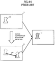
- the motion compensation inter-frame predicting coding method further comprises a step of estimating the person image 10 in the current picture 12 with the aid of the motion vector MV and pel data defining the person image 10 in the reference picture 11. In this case, there is produced only one significant pel data region 13 as shown in FIG. 44. Accordingly, the motion compensation inter-frame predicting coding method is superior to the basic inter-frame predicting coding method in the fact that the number of the significant pels can be sharply decreased and accordingly that the compression efficiency can be extremely enhanced.
- the motion compensation inter-frame predicting coding method comprises steps of dividing a current picture 20 shown in FIG. 45 into a plurality of blocks including a block (referred to hereinlater as a current block) 21, specifying a search window 31 including blocks (referred to hereinlater as candidate blocks) in a reference picture 30, and calculating distortion values each indicative a difference between the current block 21 and each of the candidate blocks.
- ITU-T International telecommunication Union-Telecommunication Standardization Sector
- the distortion value is calculated by converting, into positive numbers, local distortion values each indicative of a difference between pel data of each pel of the current block 21 and pel data of each pel of the candidate block corresponding in position to each other, and summing up the converted local distortion values.
- the motion compensation inter-frame predicting coding method further comprises steps of specifying a candidate block 32 which provides a minimum distortion value, i.e. the smallest in the distortion values calculated in the above mentioned manner, and calculating a motion vector representative of a distance between and a direction defined by the current block 21 and the candidate block 32.
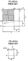
- FIGS. 46(a) and 46(b) represent relations between the current block 21, search window 31 and candidate blocks 32. If the current block 21 and the search window 31 contain N columns of M pels and L columns H pels as shown in FIGS. 46(b) and 46(a), respectively.
- the search window 31 includes (L-M+1) ⁇ (H-N+1) candidate blocks 32 similar to the current blocks 21. In the case that pel data of a pel at the top left-hand corner of current block 21 in FIG. 46(b) is indicated by a(0,0), pel data of each of the candidate blocks 32 corresponding in position to the pel data a(0,0) of the current block 21 are included in an area defined by oblique lines in FIG. 46 (a).
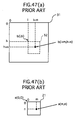
- FIGS. 47 (a) and 47 (b) represent a relations between pel data of the current block 21 and pel data of each of the candidate block 32 corresponding in position to each other.
- b(l+m, h+n) in Fig. 34(a) is indicated pel data of each of the candidate blocks corresponding in position to the pel data a(m, n)of the current block 21 shown in FIG. 47(b).
- Pel data b(l,h) in the search window 31 shown in FIG. 47 (a) is pel data at the upper left-hand corner of the candidate block 32 and accordingly corresponds in position to the pel data a(0, 0) of the current block 21.
- the norm arithmetic is absolute-value arithmetic, square arithmetic or the like.
- the above-mentioned process of comparing a block of the current picture with each of blocks of the reference picture in motion compensation inter-frame predicting coding method is so-called as a block matching method, particularly as a full search block matching method if the current block is compared with all the candidate blocks included in the search window.
- MPEG Motion Picture Experts Group
- MPEG2 Motion Picture Experts Group
- ISO/IEC International Organization for Standardization /International Electrotechnical Commission 11172-2 and 13818-2
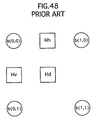
- the MPEG generates and handles half-pels each interposed between the adjoining integer pels.
- Four integer pels b(0,0), b(0,1), b(1,0) and b(1,1) are shown in FIG. 48 as forming a matrix array indicated by two columns of two pels.
- the generation of the half-pels makes it possible to search, from the search window, the candidate blocks horizontally, vertically and diagonally aligned at not one-pel pitches but half-pel pitches in the search window, so that the precision of the motion estimation can be enhanced more and more.
- the MPEG prepares the motion estimation a bi-directional prediction mode utilizing not only a forward prediction mode wherein the current picture is estimated with reference to the past picture, but also a backward prediction mode wherein the current picture is estimated with reference to the future picture.
- the implementation results of the forward and backward prediction modes are compared in prediction ability with each other. Between the forward prediction and the backward prediction is chosen one superior to the other. The implementation of the chosen mode is adopted, so that the prediction ability can be enhanced.
- the MPEG also prepares the motion estimation a bi-directional interpolation prediction mode wherein the current picture is estimated with reference to an interpolated picture that is representative of a mean between the past picture and the future picture.
- the bi-directional interpolation prediction mode is used in order to further enhance the prediction ability in comparison with the bi-directional prediction mode.
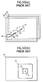
- the interpolated picture is formed depending upon a way which is described hereinafter with reference to FIGS. 50(a) and 50(b).
- reference numerals 50, 60 and 70 designate the current picture, a first reference picture previous to the current picture and a second reference picture subsequent to the current picture, respectively.
- a reference block B included in the first reference picture 60 and most similar to a current block A included in the current picture 50 is specified, thereby obtaining a motion vector MV indicative of a displacement between the reference block B and the current block A.
- the motion vector MV is scaled with respect to the second reference picture 70 to obtain a scaled vector SV.
- the motion vector MV is identical with the scaled vector SV because of the fact that a time-lag between the current picture 50 and the first reference picture 60 is equal to that between the current picture 50 and the second reference picture 70.
- a search window 72 partially forming the second reference picture 70 is specified. The search window 72 extends from a pel 71 included in the second reference picture 70 and most close to the end point of the scaled vector SV.
- the search window 72 includes a plurality of reference blocks C1, C2 ... Cn.
- interpolated blocks Dn (not shown) each indicative of a mean between the reference block 62 and each of the reference blocks Cn are calculated.
- the distortion values each indicative of a difference between each of the interpolated blocks Dn and the current block A are calculated by an expression indicated by ⁇ Dn-A ⁇ . This means that the number of the distortion values is "n".
- the minimum distortion value is selected from among the distortion values, and as a consequence a target interpolated block is specified from the interpolated blocks Dn.
- the MPEG further prepares the motion estimation a dual-prime prediction mode partly described hereinafter.
- reference numerals 81 and 82 designate a first field and a second field, respectively, of a current picture
- reference numerals 91 and 92 designate a first field and a second filed, respectively, of a reference picture.
- the current picture has a current block which consists of a field block 81a included in the first field 81 and a field block 82b included in the second field 82.
- the dual-prime prediction mode comprises a step of applying the aforementioned motion compensation inter-frame prediction to an estimation of the field block 81a with reference to the first field 91 of the reference picture to calculate a field motion vector FV.
- the field motion vector FV is scaled with respect to the second field 92 of the reference picture to obtain a scaled vector SV1.
- a search window for the motion estimation is formed by nine overlapping field blocks surrounding the half-pel 92.
- the nine field blocks consist of a center reference block including a half-pel 92P as an uppermost pel, and eight field blocks deviated vertically, horizontally and diagonally by half-pel pitch from the center reference block.
- the dual-prime prediction mode further comprises steps of calculating interpolated blocks each indicative of a mean between the reference block 91a of the first field 91 and each of the nine reference blocks included in the search window, and calculating distortion values each indicative of each interpolated block and the current block 81a. From among the calculated distortion values, the minimum distortion value is selected to obtain a differential motion vector representative of a displacement between the half-pel 92P and the uppermost pel of the reference block of the second field 92 which is used for the calculation of the minimum distortion value. In case that a reference block 92a is used for the calculation of the minimum distortion value, a vector DMV shown in FIG. 51 serves as the differential motion vector.
- the field motion vector FV is shifted from the field block 81a to the field block 82b until the endpoint of the field motion vector FV is coincided with the uppermost pel of the field block 82b.
- the shifted field block FV is denoted by "FV'" in FIG. 51.
- FV' By the starting point of the field motion vector FV' is specified a field block 92b of the second field 92.
- the field motion vector FV' is scaled with respect to the first field 91 of the reference picture to obtain a scaled vector SV2 so that a half-pel 91P of the first field 91 most closed to the starting point of the scaled vector SV2 is specified.
- the differential motion vector DMV is shifted from the half-pel 92P to the half-pel 91P, and consequently a field block 91b is specified.
- an interpolated block indicative of a mean between the field block 91b of the first field 91 and the field block 92b.
- a distortion value indicative of a difference between those blocks is calculated.
- the field motion vector FV and the differential motion vector DMV serve as motion vectors for the motion estimation.
- a drawback is encountered in the motion estimation according to a prior-art bi-directional interpolation prediction in that not only an apparatus or a circuit for performing the motion estimation becomes extremely large but also the motion vector calculation takes extremely long time. The reason is that it is required not only to calculate the distortion values the number of which is equal to that of the candidate blocks Cn included in the search window, but also to calculate the interpolated blocks the number of which is equal to that of the candidate blocks.
- the same drawback is encountered in the motion estimation according to a prior-art dual-prime prediction because of the fact that it is required to calculate the interpolated blocks the number of which is equal to that of candidate blocks.
- the present invention contemplates provision of a motion estimation method and apparatus overcoming the drawbacks of prior-art motion estimation method and apparatus of the described general nature.
- a motion estimation method for calculating a motion vector to estimate a current picture partially forming a video sequence on the basis of first and second reference pictures partially forming the video sequence.
- the current picture is partially formed by a current block including a plurality of pels represented by pel data sets, respectively.
- the first reference picture is formed by reference blocks each equal in size to the current block.
- Each of the reference blocks of the first reference picture includes a plurality of pels represented by pel data sets, respectively.
- the second reference picture is formed by reference blocks each equal in size to the current block.
- Each of the reference blocks of the second reference picture includes a plurality of pels represented by pel data sets, respectively.
- the motion vector is indicative of a displacement between the current block and one of the reference blocks of the second reference picture.
- the method comprises a step (a) of specifying a reference block similar to the current block from among the reference blocks of the first reference picture, a step (b) of multiplying each pel data set of the specified reference block by a first coefficient, a step (c) of obtaining a template block by calculating pel data sets each indicative of a difference between each multiplied pel data set of the specified reference block and each pel data set of the current block corresponding in position to each other, a step (d) of specifying part or the whole of the second reference picture as a search window, and a step (e) of obtaining candidate blocks by multiplying, by a second coefficient, each of the pel data sets of the reference blocks included in the search window, and a step (f) of calculating, on the basis of the pel data sets of each of candidate blocks and the pel data sets of the template block, distortion values each indicative of a difference between each of interpol
- Each of the interpolated blocks is indicative of a mean between the specified reference block of the first reference picture and each of the reference blocks of the search window.
- the method further comprises a step (g) of selecting a minimum distortion value from among the distortion values, and a step (h) of specifying a reference block of the second reference picture bringing the minimum distortion value to obtain the motion vector.
- a motion estimation apparatus for calculating a motion vector to estimate a current picture partially forming a video sequence on the basis of first and second reference pictures partially forming the video sequence.
- the current picture is partially formed by a current block including a plurality of pels represented by pel data sets, respectively.
- the first reference picture is formed by reference blocks each equal in size to the current block.
- Each of the reference blocks of the first reference picture includes a plurality of pels represented by pel data sets, respectively.
- the second reference picture is formed by reference blocks each equal in size to the current block.
- Each of the reference blocks of the second reference picture includes a plurality of pels represented by pel data sets, respectively.
- the motion vector is indicative of a displacement between the current block and one of the reference blocks of the second reference picture.
- the apparatus comprises block specifying means for specifying a reference block similar to the current block from among the reference blocks of the first reference picture, and template block obtaining means for obtaining a template block by multiplying each pel data set of the specified reference block by a first coefficient and by calculating pel data sets each indicative of a difference between each multiplied pel data set of the specified reference block and each pel data set of the current block corresponding in position to each other.
- the apparatus further comprises search window specifying means for specifying part or the whole of the second reference picture as a search window, candidate block obtaining means for obtaining candidate blocks by multiplying, by a second coefficient, each of the pel data sets of the reference blocks included in the search window, and distortion calculating means for calculating, on the basis of the pel data sets of each of candidate blocks and the pel data sets of the template block, distortion values each indicative of a difference between each of interpolated blocks and the current block.
- Each of the interpolated blocks is indicative of a mean between the specified reference block of the first reference picture and each of the reference blocks of the search window.
- the apparatus further comprises distortion selecting means for selecting a minimum distortion value from among the distortion values, and motion vector calculating means for calculating the motion vector by specifying a reference block of the second reference picture bringing the minimum distortion value.
- a motion estimation apparatus for calculating a motion vector to estimate a current picture partially forming a video sequence on the basis of first and second reference pictures partially forming the video sequence.
- the current picture is partially formed by a current block including a plurality of pels represented by pel data sets, respectively.
- the first reference picture is formed by reference blocks each equal in size to the current block.
- Each of the reference blocks of the first reference picture includes a plurality of pels represented by pel data sets, respectively.
- the second reference picture is formed by reference blocks each equal in size to the current block.
- Each of the reference blocks of the second reference picture includes a plurality of pels represented by pel data sets, respectively.
- the motion vector is indicative of a displacement between the current block and one of the reference blocks of the second reference picture.
- the apparatus comprises block specifying means for specifying a reference block similar to the current block from among the reference blocks of the first reference picture provisional template block obtaining means for obtaining a provisional template block by multiplying each pel data set of the specified reference block by a first coefficient and by subtracting the multiplied pel data sets of the specified reference block from the pel data sets of the current block, respectively, and first selecting means for selecting one from the current block and the provisional template block and outputting the selected current block as a template block.
- the apparatus further comprises search window specifying means for specifying part or the whole of the second reference picture as a search window, provisional candidate block obtaining means for obtaining provisional candidate blocks by multiplying, by a second coefficient, each pel data set of the reference blocks included in the search window, and second selecting means for selecting one from a group of the reference blocks and a group of the provisional candidate blocks and outputting the selected reference blocks as candidate blocks.
- the reference blocks is selected when the current blocks are selected by the provisional template block obtaining means.
- the provisional candidate blocks are selected when the provisional template blocks are selected by the provisional template block obtaining means.
- the apparatus further comprises distortion calculating means for calculating, on the basis of the pel data sets of each of candidate blocks and the pel data sets of the template block, distortion values each indicative of a difference between each of interpolated blocks and the current block.
- Each of the interpolated blocks is indicative of a mean between the specified reference block of the first reference picture and each of the reference blocks of the search window.
- the apparatus further comprises distortion selecting means for selecting a minimum distortion value from among the distortion values, and motion vector calculating means for calculating the motion vector by specifying a reference block of the second reference picture bringing the minimum distortion value.
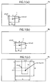
- the motion estimation apparatus is designed to calculate a motion vector to estimate a current picture Pa shown in FIG. 1(a) on the basis of first and second reference pictures Pb and Pc shown in FIGS. 1(b) and 1(c), respectively.
- the current picture Pa and the first and second reference pictures Pb and Pc partially form a video sequence.
- the current picture Pa is partially formed by a current block 1 including a plurality of integer pels represented by pel data sets, respectively.
- the first reference picture Pb is formed by reference blocks including a reference block 2.
- Each of the reference blocks of the first reference picture Pb is equal in size to the current block 1 and includes a plurality of integer pels represented by pel data sets, respectively.
- the second reference picture Pc is formed by reference blocks. Each of the reference blocks of the second reference picture Pc is equal in size to the current block Pa and includes a plurality of integer pels represented by pel data sets, respectively.
- the motion vector is indicative of a displacement between the current block 1 and a selected reference block of the second reference picture Pc. The selected reference block will become apparent as the description proceeds.
- the motion estimation apparatus is shown in FIG. 2 as comprising block specifying means 100, template block obtaining means 200a, search window specifying means 300, candidate block obtaining means 400, distortion calculating means 1000a, distortion selecting means 500 and motion vector calculating means 600.
- the block specifying means 100 is operated to specify one most similar to the current block 1 from among the reference blocks of the first reference picture Pb and to output integer pel data sets of the specified reference block. It is assumed that the specified reference block is the reference block 2 and that the pel data sets of the current block 1 and the reference block 2 are represented by a(m,n) and b(m,n), respectively, as shown in FIGS. 1(a) and 1(b).
- the specifying operation may be carried out by using of a motion compensation inter-frame predictive coding algorithm described hereinbefore with reference to FIGS. 45 through 47.
- the template block obtaining means 200a is operated to receive the integer pel data sets b(m,n) of the reference block 2 from the block specifying means 100 and subsequently to multiply each of the integer pel data sets b(m,n) by a first coefficient E.
- the template block obtaining means 200a is further operated to calculate a difference between each of the pel data sets a(m,n) of the current block 1 and each of the multiplied data sets b(m,n) ⁇ E corresponding in position to each other by subtracting each of the pel data sets b(m,n) ⁇ E from the each of the pel data sets a(m,n). Therefore, the difference is a(m,n)-b(m,n) ⁇ E .
- the search window specifying means 300 is operated to specify part or the whole of the second reference picture Pc as the search window. It is assumed that the specified search window is a search window denoted by reference numeral 3 in FIG. 3. Preferably, the search window 3 may be specified on the basis of a displacement between the current block 1 and the specified reference block 2. More specifically, the search window specifying means 300 is operated to calculate a motion vector indicative of the displacement between the current block 1 and the specified reference block 2, and scaling the motion vector with respect to the second reference picture Pc to obtain a point on the second reference picture Pc The search window 3 is specified so as to include and extending from the obtained point. The search window 3 includes part of the reference blocks of the second reference picture Pc. Each of the reference blocks included in the search window 3 are designated by reference numeral 3c and is represented by integer pels respectively having pel data sets c(x+m,y+n) .
- the candidate block obtaining means 400 is operated to receive the pel data sets c(x+m,y+n) of each of the reference blocks 3c from the search window specifying means 300 and to multiply each of the pel data sets c(x+m,y+n) by a second coefficient F, for obtaining candidate blocks. This means that each of the candidate blocks has the pel data sets c(x+m,y+n) ⁇ F .
- the distortion calculating means 1000a is operated to calculate distortion values each indicative of a difference between the current block 1 and each of interpolated blocks by subtracting each pel data set a(m,n)-b(m,n) ⁇ E of the template block from each pel data set c(x+m,y+n) ⁇ F of each of the candidate blocks, converting the subtracted data sets to positive data sets, and summing up the positive data sets in one block unit for calculating distortion values each indicative of a difference between each of the interpolated blocks and the current block 1.
- the distortion selecting means 500 is operated to select the minimum distortion value from among the distortion values calculated by the distortion calculating means 1000a.
- the motion vector calculating means 600 is operated to calculate the motion vector by specifying one of reference blocks 3c included in the search window 3.
- the specified reference block of the search window 3 defines, in cooperation with the specified reference block 2 of the first reference picture Pb, the interpolated block bringing the minimum distortion value selected by the distortion selecting means 500.
- the distortion calculating means 1000a comprises pel data outputting means 1020, first difference calculating means 1031, second difference calculating means 1032, third difference calculating means 1033, fourth difference calculating means 1034, first converting means 1041, a second converting means 1042, a third converting means 1043, fourth converting means 1044, first distortion calculating means 1110, second distortion calculating means 1120, third distortion calculating means 1130 and fourth distortion calculating means 1140.
- the candidate blocks will be described hereinafter in detail.
- the candidate blocks consist of first candidate blocks, second candidate blocks each vertically deviated by half-pel pitch from each of the first candidate blocks, third candidate blocks each horizontally deviated by half-pel pitch from each of the first candidate blocks, and fourth candidate blocks each diagonally deviated by half-pel pitch from each of the first candidate blocks.
- the first candidate blocks are formed by integer pels
- the second, third and fourth candidate blocks are formed by half-pels interposed between two of integer pels adjacent to each other.
- the integer pels of the first candidate blocks are represented by integer pel data sets, respectively
- the half pels of each of the second, third and fourth candidate blocks are represented by half pel data sets, respectively. Therefore, the distortion values consist of first distortion values based on the first candidate blocks, second distortion values based on the second candidate blocks, respectively, third distortion values based on the third candidate blocks, respectively, and fourth distortion values based on the fourth candidate blocks, respectively.
- the pel data outputting means 1020 is operated to receive the integer pel data sets a(m,n)-b(m,n) ⁇ E of the template block from the template block data calculating means 200a and the integer pel data sets c(x+m,y+n) ⁇ F of the first candidate block from the candidate block data calculating means 400.
- the pel data outputting means 1020 is further operated to output a pair of the integer pel data sets of the template block and the candidate block corresponding in position to each other to the first difference data calculating means 1031.
- the first difference data calculating means 1031 is operated to subtract the pel data sets a(m,n)-b(m,n) ⁇ E of the template block from the pel data sets c(x+m,y+n) ⁇ F of each candidate block, for calculating first difference data sets ⁇ c(x+m,y+n) ⁇ F ⁇ - ⁇ a(m,n)-b(m,n) ⁇ E ⁇ .
- the first converting means 1041 is operated to convert the first difference data sets to positive data sets
- the first distortion calculating means 1110 is operated to calculate the sum of the converted first difference data sets based on each of the candidate blocks to obtain each of the first distortion values.
- each of the first distortion values is indicative of a difference between each first interpolated block and the current block 1
- the second difference data calculating means 1032 is operated to calculate the sum of two of the first difference data sets ⁇ c(x+m,y+n) ⁇ F ⁇ - ⁇ a(m,n)-b(m,n) ⁇ E ⁇ and ⁇ c(x+m,y+1+n) ⁇ F ⁇ - ⁇ a(m,n)-b(m,n) ⁇ E ⁇ vertically deviated by half-pel pitch from each other and multiply the sum by 1/2 to obtain second difference data sets [ ⁇ c(x+m,y+n) ⁇ F ⁇ - ⁇ a(m,n)-b(m,n) ⁇ E ⁇ + ⁇ c(x+m,y+1+n) ⁇ F ⁇ - ⁇ a(m,n)-b(m,n) ⁇ E ⁇ ]/2 .
- the second converting means 1042 is operated to convert the second difference data sets to positive data sets
- the second distortion calculating means 1120 is operated to calculate the sum of the converted second difference data sets based on each of the candidate blocks to obtain each of the second distortion values.
- each of the second distortion values is indicative of a difference between each second interpolated block and the current block 1
- the third difference data calculating means 1033 is operated to calculate the sum of two of the first difference data sets ⁇ c(x+m,y+n) ⁇ F ⁇ - ⁇ a(m,n)-b(m,n) ⁇ E ⁇ and ⁇ c(x+1+m,y+n) ⁇ F ⁇ - ⁇ a(m,n)-b(m,n) ⁇ E ⁇ horizontally deviated by half-pel pitch from each other and multiply the sum by 1/2 to obtain third difference data sets [ ⁇ c(x+m,y+n) ⁇ F ⁇ - ⁇ a(m,n)-b(m,n) ⁇ E ⁇ + ⁇ c(x+1+m,y+n) ⁇ F ⁇ - ⁇ a(m,n)-b(m,n) ⁇ E ⁇ ]/2 .
- the third converting means 1043 is designed to convert the third difference data sets to positive data sets
- the third distortion calculating means 1130 is designed to calculate the sum of the converted third difference data sets based on each of the candidate blocks 6 to obtain each of the third distortion values.
- each of the third distortion values is indicative of a difference between each third interpolated block and the current block 1
- the fourth difference data calculating means 1034 is operated to calculate the sum of two of the third difference data sets [ ⁇ c(x+m,y+n) ⁇ F ⁇ - ⁇ a(m,n)-b(m,n) ⁇ E ⁇ + c(x+1+m,y+n) ⁇ F ⁇ - ⁇ a(m,n)-b(m,n) ⁇ E ⁇ ]/2 and [ ⁇ c(x+m,y+1+n)xF ⁇ - ⁇ a(m,n)-b(m,n) ⁇ E ⁇ + ⁇ c(x+1+m,y+1+n) ⁇ F ⁇ - ⁇ a(m,n)- b(m,n) ⁇ E ⁇ ]/2 vertically deviated by half-pel pitch from each other and multiply the sum by 1/2 to obtain fourth difference data sets [[ ⁇ c(x+m,y+n) ⁇ F ⁇ - ⁇ a(m,n)- b(m,n) ⁇ E ⁇ + c(x+1+m,y+n) ⁇ F ⁇ - ⁇ a(m,n)-b(m,
- the fourth converting means 1044 is operated to convert the fourth difference data sets to positive data sets
- the fourth distortion calculating means 1140 is designed to calculate the sum of the converted fourth difference data sets based on each of the candidate blocks to obtain each of the fourth distortion values.
- each of the fourth distortion values is indicative of a difference between each fourth interpolated block and the current block 1
- the aforementioned motion estimation apparatus will be described hereinafter in the concrete.
- the current picture Pa, the first reference picture Pb and the second reference picture Pc are shown in FIGS. 4(a), 4(b) and 4(c) as including the current block 1, the specified reference block 2 and the search window 3, respectively, shown in the concrete.
- both M and N are set to "2" and that both L and H are set to "4".
- the first and second coefficient are set to "1/2".
- the integer pels of the current block 1 are represented by integer pel data sets indicated by a(0,0), a(0,1), a(1,0) and a(1,1), respectively, as shown in FIG. 4(a).
- the integer pels of the reference block 2 are represented by integer pel data sets indicated by b(0,0), b(0,1), b(1,0) and b(1,1), respectively, as shown in FIG. 4(b).
- the template block 4a is shown in FIG. 5.
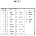
- the integer pels of the search window 3 are represented by integer pel data sets indicated by c(0,0), c(0,1), c(0,2), c(0,3), c(1,0), c(1,1), c(1,2), c(1,3), c(2,0), c(2,1), c(2,2), c(2,3), c(3,0), c(3,1), c(3,2) and c(3,3), respectively, as shown in FIG. 4(c).
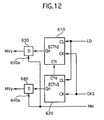
- the motion estimation apparatus is shown in FIG. 7 as further comprising a timing control unit 900 provided with signal output terminals P1 to P9 through which a clock signal CK1 and control signals LD, CK2, CLE, SU, SL, Si, UMASK and CK3 are outputted, respectively.
- the clock signal CK1 and the control signals CK2, CLE, SU and SL are transmitted to the distortion calculating means 1000a.
- the control signal LD is transmitted to the distortion calculating means 1000a, the distortion selecting means 500 and the motion vector calculating means 600.
- the control signals Si and UMASK are transmitted to the distortion selecting means 500.
- the control signal CK3 is transmitted to the distortion selecting means 500 and the motion vector calculating means 600.
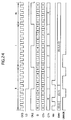
- the signals CK1, LD, CK2, CLE, SU, SL, Si, UMASK and CK3 are illustrated in FIGS. 13 and 24.
- the clock signal CK1 comprises clock pulses which not only serve as criteria of the control signals LD, CK2, CLE, SU, Si, UMASK and CK3 but also is used for regulation of the operations of the distortion calculating means 1000a, the distortion selecting means 500 and the motion vector calculating means 600.
- the control signal LD comprises a first pulse outputted in step with the sixth clock pulse of the clock signal CK1, and subsequent pulses outputted at a rate of one pulse per the four clock pulses of the clock signal CK1.
- Each of the pluses of the control signal LD is twice the width of that of the clock signal CK1.
- the control signal CK2 is formed similarly to the clock signal CK1.
- the control signal CLE comprises a first pulse outputted in step with the sixth clock pulse of the clock signal CK1, and subsequent pulses outputted at a rate of one pulse per the four clock pulses of the clock signal CK1.
- Each of the pluses of the control signal CLE is twice the width of that of the clock signal CK1.
- the control signal SU comprises a first pulse outputted in step with the second clock pulse of the clock signal CK1, and subsequent pulses outputted at a rate of one pulse per the four clock pulses of the clock signal CK1.
- Each of the pluses of the control signal SU is four times the width of that of the clock signal CK1.
- the control signal SL comprises a first pulse outputted in step with the first clock pulse of the clock signal CK1, and subsequent pulses outputted at a rate of one pulse per the two clock pulses of the clock signal CK1.
- Each of the pluses of the control signal SL is twice the width of that of the clock signal CK1.
- the control signal Si comprises count signals represented by "0" to "9".
- the count signals consist of a first count signal outputted in step with the eleventh clock pulse of the clock signal CK1, and subsequent count signals outputted in step with the pulse of the control signal CK3.
- the control signal UMASK comprises pulses outputted in accordance with a predetermined internal pattern to restrict the candidate blocks 6 to be compared with one another.
- the control signal CK3 comprises a first pulse outputted in step with the first clock pulse of the clock signal CK1, and subsequent pulses outputted at a rate of ten pulses per the one clock pulse of the clock signal CK1.
- Each of the pluses of the control signal CK3 is 1/10 times the width of that of the clock signal CK1.
- the template block obtaining means 200a is shown in FIG. 8 as comprising a multiplier 210 and a subtracter 220.
- the multiplier 210 has a data input terminal and a data output terminal.
- the multiplier 210 is designed to multiply data on the data input terminal by the first coefficient "1/2" and output the multiplied data through the data output terminal.
- the subtracter 220 has a first data input terminal A, a second data input terminal B and a data output terminal.
- the subtracter 220 is adapted to subtract data on the first data input terminal A from data on the second data input terminal B and output the subtracted data through the data output terminal.
- the data input terminal of the multiplier 210 is electrically connected to the data output terminal of the block data outputting means 100.
- the first data input terminal A of the subtracter 220 is electrically connected to the data output terminal of the multiplier 210, while the second data input terminal B of the subtracter 220 is electrically connected to a data output terminal (not shown) of the current block data outputting means.
- the pel data sets b(0,0), b(0,1), b(1,1) and b(1,0) are received in described order by the data input terminal of the multiplier 210 from the block specifying means 100.
- the multiplied data sets b(0,0)/2, b(0,1)/2, b(1,1)/2 and b(1,0)/2 are received in described order by the first data input terminal A of the subtracter 220 from the multiplier 210, while the pel data sets a(0,0), a(0,1), a(1,1) and a(1,0) are received in described order by the second data input terminal B of the subtracter 220 from the current block data outputting means.
- the candidate block obtaining means 400 is shown in FIG. 8 as comprising a pair of multipliers 411 and 412.
- Each of the multipliers 411 and 412 has a data input terminal and a data output terminal.
- Each of the multipliers 411 and 412 is designed to multiply data on the data input terminal by the second coefficient "1/2" and outputs the multiplied data through the data output terminal.
- the data input terminals of the multipliers 411 and 412 are electrically connected to data output terminals (not shown), respectively, of the search window specifying means 300.
- the pel data sets c(0,1), c(0,0), c(1,0), c(1,1), c(2,1), c(2,0), c(3,0) and c(3,1) are received in described order by the data input terminal of the multiplier 411 from the search window specifying means 300.
- the pel data sets c(0,1)/2, c(0,0)/2, c(1,0)/2, c(1,1)/2, c(2,1)/2, c(2,0)/2, c(3,0)/2 and c(3,1)/2 are outputted in described order through the data output terminal of the multiplier 411.
- the pel data sets c(0,3), c(0,2), c(1,2), c(1,3), c(2,3), c(2,2), c(3,2) and c(3,3) are received in described order by the data input terminal of the multiplier 412 from the search window specifying means 300.
- step with the pulses of the clock signal CK1 in the periods (a) to (h) as shown in FIG. 13, the pel data sets c(0,3)/2, c(0,2)/2, c(1,2)/2, c(1,3)/2, c(2,3)/2, c(2,2)/2, c(3,2)/2 and c(3,3)/2 are outputted in described order through the data output terminal of the multiplier 412.
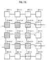
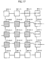
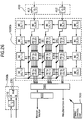
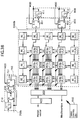
- the distortion calculating means 1000a comprises nine processor elements PE1a(0,0), PE1a(0,1), PE1a(0,2), PE1a(1,0), PE1a(1,1), PE1a(1,2), PE1a(2,0), PE1a(2,1), PE1a(2,2) and eleven shift registers RE(0,-1), RE(1,-1), RE(2,-1), RE(3,-1), RE(3,0), RE(3,1), RE(3,2), RE(0,3), RE(1,3), RE(2,3), RE(3,3).
- FIG. 9 is a plan view of each of the processor element PE1a(x,y).
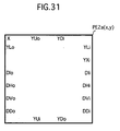
- each of the processor elements PE1a(x,y) has data input terminals X YDi, YLi, HLi, DIi, DHi, DVi, DDi, HXi, HUi and YUi, data output terminals YUo, HUo, HXo, YDo, DDo, DVo, DHo, DIo, HLo and YLo, signal input terminals (not shown) and signal output terminals (not shown).
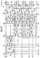
- Each of the processor elements PE1a(x,y) is shown in FIG. 10 as comprising a selector 1301, a D flip-flop 1302, a subtracter 1303, a positive value transducer 1305, an adder 1306, a D flip-flop 1307, a selector 1308 and a D flip-flop 1309.
- the selector 1301 has a first data input terminal A, a second data input terminal B, a third data input terminal C, first and second signal input terminals S0 and S1, and a data output terminal Y.
- first and second signal input terminals S0 and S1 of the selector 1301 receive signals representative of "0" and "0", respectively, data on the first data input terminal A of the selector 1301 are selected and outputted through the data output terminal Y of the selector 1301.
- the first and second signal input terminals S0 and S1 of the selector 1301 receive signals representative of "1" and "0", respectively, data on the second data input terminal B of the selector 1301 are selected and outputted through the data output terminal Y of the selector 1301.
- the D flip-flop 1302 has data input terminal, a signal input terminal 1302a and a data output terminal.
- the D flip-flop 1302 detects a rising edge of a pulse received by the signal input terminal 1302a, i.e., when a signal received by the signal input terminal 1302a of the D flip-flop 1302 is changed "0" to "1"
- the D flip-flop 1302 latches, on the data output terminal, data received at that time by the data input terminal.
- the subtracter 1303 has a first data input terminal A, a second data input terminal B and a data output terminal. The subtracter 1303 is adapted to subtract data received by the second data input terminal B from data received by the first data input terminal A and output the subtracted data through the data output terminal.
- the positive value transducer 1305 has a data input terminal and a data output terminal.
- the positive value transducer 1305 is an absolute value transducer or a square multiplier. If the positive value transducer 1305 is the absolute value transducer, the positive value transducer 1305 converts data on the data input terminal to positive value data by means of absolute value arithmetic and outputs the converted data through the data output terminal. If the positive value transducer 1305 is the square multiplier, the positive value transducer 1305 converts data on the data input terminal to positive value data by means of square arithmetic and outputs the converted data through the data output terminal.
- the adder 1306 has a first data input terminal A, a second data input terminal B and a data output terminal. The adder 1306 is designed to add data on the second data input terminal B to data on the first data input terminal A and output the added data through the data output terminal.
- the D flip-flop 1307 has a data input terminal, a first signal input terminal 1307a, a second signal input terminal 1307b and a data output terminal.
- the D flip-flop 1307 detects a low-to-high transition of a signal received by the first signal input terminal 1307a, the D flip-flop latches, on the data output terminal, data received at that time by the data input terminal.
- the D flip-flop 1307 detects a low-to-high transition of a signal received by the second signal input terminal 1307b
- the D flip-flop 1307 resets data on the data output terminal to "0".
- the selector 1308 has a first data input terminal A, a second data input terminal B, a signal input terminal S and a data output terminal Y.
- the signal input terminal S of the selector 1308 receives a signal representative of "0”
- data on the first data input terminal A of the selector 1308 are selected and outputted through the data output terminal Y of the selector 1308.
- the signal input terminal S of the selector 1308 receives a signal representative of "1”
- data on the second data input terminal B of the selector 1308 are selected and outputted through the data output terminal Y of the selector 1308.
- the D flip-flop 1309 has a data input terminal, a signal input terminal 1309a and a data output terminal. When the D flip-flop 1309 detects a rising edge of a pulse received by the signal input terminal 1309a, the D flip-flop 1309 latches, on the data output terminal, data received at that time by the data input terminal.
- the first data input terminal A of the selector 1301 of the present processor element PE1a(x,y) is electrically connected to the data output terminal of the D flip-flop 1302 of the upper side processor element PE(x,y-1) through the data input terminal YDi of the present processor element PE1a(x,y) and the data output terminal YDo of the upper side processor element PE1a(x,y-1). If there is no upper side processor element PE1a(x,y-1), the first data input terminal A of the selector 1301 of the present processor element PE1a(x,y) is electrically connected to a data output terminal of the upper side shift register RE(x,y-1) through the data input terminal YDi of the present processor element PE1a(x,y).
- the second data input terminal B of the selector 1301 of the present processor element PE1a(x,y) is electrically connected to the data output terminal of the lower side processor element PE1a(x,y+1) through the data input terminal YUi of the present processor element PE1a(x,y) and the data output terminal YUo of the lower side processor element PE1a(x,y+1). If there is no lower side processor element PE1a(x,y+1), the second data input terminal B of the selector 1301 of the present processor element PE1a(x,y) is electrically connected to the data output terminal of the lower side shift register RE(x,y+1) through the data input terminal YUi of the present processor element PE1a(x,y).
- the third data input terminal C of the selector 1301 of the present processor element PE1a(x,y) is electrically connected to the data output terminal of the right side processor element PE1a(x+1,y) through the data input terminal YLi of the present processor element PE1a(x,y) and the data output terminal YLo of the right side processor element PE1a(x+1,y). If there is no right side processor element PE1a(x+1,y), the third data input terminal C of the selector 1301 of the present processor element PE1a(x,y) is electrically connected to a data output terminal of the right side shift register RE(x+1,y) through the data input terminal YLi of the present processor element PE1a(x,y).
- the first signal input terminal S0 of the selector 1301 of the present processor element PE1a(x,y) is electrically connected to the signal output terminal of the timing control unit 900 to receive the control signal SU, while the second signal input terminal S1 of the selector 1301 of the present processor element PE1a(x,y) is electrically connected to the signal output terminal of the timing control unit 900 to receive the control signal SL.
- the data input terminal of the D flip-flop 1302 of the present processor element PE1a(x,y) is electrically connected to the data output terminal Y of the selector 1301 of the present processor element PE1a(x,y).
- the signal input terminal 1302a of the D flip-flop 1302 of the present processor element PE1a(x,y) is electrically connected to the signal output terminal of the timing control unit 900 to receive the clock signal CK1.
- the first data input terminal A of the subtracter 1303 of the present processor element PE1a(x,y) is electrically connected to the data output terminal of the D flip-flop 1302 of the present processor element PE1a(x,y), while the second data input terminal B of the subtracter 1303 of the present processor element PE1a(x, y) is electrically connected to the data output terminal of the template block obtaining means 200 through the data input terminal X of the present processor element PE1a(x,y).
- the data input terminal of the positive value transducer 1305 of the present processor element PE1a(x,y) is electrically connected to the data output terminal of the subtracter 1303 of the present processor element PE1a(x,y).
- the first input terminal A of the adder 1306 of the present processor element PE1a(x,y) is electrically connected to the data output terminal of the positive value transducer 1305 of the present processor element PE1a(x,y), while the second input terminal B of the adder 1306 of the present processor element PE1a(x, y) is electrically connected to the data output terminal of the D flip-flop 1307 of the present processor element PE1a(x,y).
- the data input terminal of the D flip-flop 1307 of the present processor element PE1a(x,y) is electrically connected to the data output terminal of the adder 1306 of the present processor element PE1a(x,y).
- the first signal input terminal 1307a of the D flip-flop 1307 is electrically connected to the signal output terminal of the timing control unit 900 to receive the clock signal CK1
- the second signal input terminal 1307b of the D flip-flop 1307 is electrically connected to the signal output terminal of the timing control unit 900 to receive the control signal CLE.
- the first data input terminal A of the selector 1308 of the present processor element PE1a(x,y) is electrically connected to the data output terminal of the D flip-flop 1309 of the right side processor element PE1a(x+1,y) through the data input terminal DIi of the present processor element PE1a(x,y) and the data output terminal DIo of the right side processor element PE1a(x+1,y), while the second data input terminal B of the selector 1308 of the present processor element PE1a(x,y) is electrically connected to the data output terminal of the D flip-flop 1307 of the present processor element PE1a(x,y).
- the signal input terminal S of the selector 1308 of the present processor element PE1a(x,y) is electrically connected to the signal output terminal of the timing control unit 900 to receive the control signal LD.
- the data input terminal of the D flip-flop 1309 is electrically connected to the data output terminal Y of the selector 1308.
- the signal input terminal 1309a of the D flip-flop 1309 is electrically connected to the signal output terminal of the timing control unit 900 to receive the control signal CK2.
- Each of the processor elements PE1a(x,y) further comprises an adder 1313, a multiplier 1314, a positive value transducer 1315, an adder 1316, a D flip-flop 1317, a selector 1318 and a D flip-flop 1319.
- the adder 1313 has a first data input terminal A, a second data input terminal B and a data output terminal.
- the adder 1313 is designed to add data on the second data input terminal B to data on the first data input terminal A and output the added data through the data output terminal.
- the multiplier 1314 has a data input terminal and a data output terminal.
- the multiplier 1314 is designed to multiply data on the data input terminal by "1/2" and outputs the multiplied data through the data output terminal.
- the positive value transducer 1315 has a data input terminal and a data output terminal.
- the positive value transducer 1315 is an absolute value transducer or a square multiplier. If the positive value transducer 1315 is the absolute value transducer, the positive value transducer 1315 converts data on the data input terminal to positive value data by means of absolute value arithmetic and outputs the converted data through the data output terminal. If the positive value transducer 1315 is the square multiplier, the positive value transducer 1315 converts data on the data input terminal to positive value data by means of square arithmetic and outputs the converted data through the data output terminal.
- the adder 1316 has a first data input terminal A, a second input terminal B and a data output terminal.
- the adder 1316 is designed to add data on the second data input terminal B to data on the first data input terminal A and output the added data through the data output terminal.
- the D flip-flop 1317 has a data input terminal, a first signal input terminal 1317a, a second signal input terminal 1317b and a data output terminal.
- the D flip-flop 1317 detects a low-to-high transition of a signal received by the first signal input terminal 1317a
- the D flip-flop 1317 latches, on the data output terminal, data received at that time by the data input terminal.
- the D flip-flop 1317 detects a low-to-high transition of a signal received by the second signal input terminal 1317b
- the D flip-flop 1317 resets data on the data output terminal to "0".
- the selector 1318 has a first data input terminal A, a second data input terminal B, a signal input terminal S and a data output terminal Y.
- the signal input terminal S of the selector 1318 receives a signal representative of "0”
- data on the first data input terminal A of the selector 1318 are selected and outputted through the data output terminal Y of the selector 1318.
- the signal input terminal S of the selector 1318 receives a signal representative of "1”
- data on the second data input terminal B of the selector 1318 are selected and outputted through the data output terminal Y of the selector 1318.
- the D flip-flop 1319 has data input terminal, a signal input terminal 1319a and a data output terminal.
- the D flip-flop 1319 detects a rising edge of a pulse received by the signal input terminal 1319a, the D flip-flop 1319 latches, on the data output terminal, data received at that time by the data input terminal.
- the first data input terminal A of the adder 1313 of the present processor element PE1a(x,y) is electrically connected to the data output terminal of the subtracter 1303 of the present processor element PE1a(x,y).
- the second data input terminal B of the adder 1313 of the present processor element PE1a(x,y) is electrically connected to the data output terminal of the subtracter 1303 of the lower side processor element PE1a(x,y+1) through the data input terminal HUi of the present processor element PE1a(x,y) and the data output terminal HUo of the lower side processor element PE1a(x,y+1).
- the second data input terminal B of the subtract 1313 of the present processor element PE1a(x,y) is electrically connected to the data output terminal of the lower side shift register RE(x,y+1) through the data input terminal HUi of the present processor element PE1a(x,y).
- the data input terminal of the multiplier 1314 of the present processor element PE1a(x,y) is electrically connected to the data output terminal of the adder 1313 of the present processor element PE1a(x,y).
- the data input terminal of the positive value transducer 1315 of the present processor element PE1a(x,y) is electrically connected to the data output terminal of the multiplier 1314 of the present processor element PE1a(x,y).
- the first data input terminal A of the adder 1316 of the present processor element PE1a(x,y) is electrically connected to the data output terminal of the positive value transducer 1315 of the present processor element PE1a(x,y), while the second data input terminal B of the adder 1316 of the present processor element PE1a(x,y) is electrically connected to the data output terminal of the D flip-flop 1317 of the present processor element PE1a(x,y).
- the data input terminal of the D flip-flop 1317 of the present processor element PE1a(x,y) is electrically connected to the data output terminal of the adder 1316 of the present processor element PE1a(x,y).
- the first signal input terminal 1317a of the D flip-flop 1317 of the present processor element PE1a(x,y) is electrically connected to the signal output terminal of the timing control unit 900 to receive the clock signal CK1, while the second signal input terminal 1317b of the D flip-flop 1317 of the present processor element PE1a(x,y) is electrically connected to timing control unit 900 to receive the control signal CLE.
- the first data input terminal A of the selector 1318 of the present processor element PE1a(x,y) is electrically connected to the data output terminal of the D flip-flop 1319 of the right side processor element PE1a(x+1,y) through the data input terminal DVi of the present processor element PE1a(x,y) and the data output terminal DVo of the right side processor element PE1a(x+1,y), while the second data input terminal B of the selector 1318 of the present processor element PE1a(x,y) is electrically connected to the data output terminal of the D flip-flop 1317 of the present processor element PE1a(x,y).
- the signal input terminal S of the selector 1318 of the present processor element PE1a(x,y) is electrically connected to the signal output terminal of the timing control unit 900 to receive the control signal LD.
- the data input terminal of the D flip-flop 1319 of the present processor element PE1a(x,y) is electrically connected to the data output terminal Y of the selector 1318 of the present processor element PE1a(x,y).
- the signal input terminal 1319a of the D flip-flop 1319 of the present processor element PE1a(x,y) is electrically connected to the signal output terminal of the timing control unit 900 to receive the control signal CK2.
- Each of the processor elements PE1a(x,y) further comprises an adder 1323, a multiplier 1324, a positive value transducer 1325, an adder 1326, a D flip-flop 1327, a selector 1328 and a D flip-flop 1329.
- the adder 1323 has a first data input terminal A, a second data input terminal B and a data output terminal.
- the adder 1323 is designed to add data on the second data input terminal B to data on the first data input terminal A and output the added data through the data output terminal.
- the multiplier 1324 has a data input terminal and a data output terminal.
- the multiplier 1324 is designed to multiply data on the data input terminal by "1/2" and outputs the multiplied data through the data output terminal.
- the positive value transducer 1325 has a data input terminal and a data output terminal.
- the positive value transducer 1325 is an absolute value transducer or a square multiplier.
- the positive value transducer 1325 converts data on the data input terminal to positive value data by means of absolute value arithmetic and outputs the converted data through the data output terminal. If the positive value transducer 1325 is the square multiplier, the positive value transducer 1325 converts data on the data input terminal to positive value data by means of square arithmetic and outputs the converted data through the data output terminal.
- the adder 1326 has a first data input terminal A, a second input terminal B and a data output terminal.
- the adder 1326 is designed to add data on the second data input terminal B to data on the first data input terminal A and output the added data through the data output terminal.
- the D flip-flop1327 has a data input terminal, a first signal input terminal 1327a, a second signal input terminal 1327b and a data output terminal.
- the D flip-flop 1327 detects a low-to-high transition of a signal received by the first signal input terminal 1327a
- the D flip-flop 1327 latches, on the data output terminal, data received at that time by the data input terminal.
- the D flip-flop 1327 detects a low-to-high transition of a signal received by the second signal input terminal 1327b
- the D flip-flop 1327 resets data on the data output terminal to "0".
- the selector 1328 has a first data input terminal A, a second data input terminal B, a signal input terminal S and a data output terminal Y.
- the signal input terminal S of the selector 1328 receives a signal representative of "0”
- data on the first data input terminal A of the selector 1328 are selected and outputted through the data output terminal Y of the selector 1328.
- the signal input terminal S of the selector 1328 receives a signal representative of "1”
- data on the second data input terminal B of the selector 1328 are selected and outputted through the data output terminal Y of the selector 1328.
- the D flip-flop 1329 has data input terminal, a signal input terminal 1329a and a data output terminal.
- the D flip-flop 1329 detects a rising edge of a pulse received by the signal input terminal 1329a, the D flip-flop 1329 latches, on the data output terminal, data received at that time by the data input terminal.
- the first data input terminal A of the adder 1323 of the present processor element PE1a(x,y) is electrically connected to the data output terminal of the subtracter 1303 of the present processor element PE1a(x,y), while the second data input terminal B of the adder 1323 of the present processor element PE1a(x,y) is electrically connected to the data output terminal of the subtracter 1303 of the right side processor element PE1a(x+1,y) through the data input terminal HLi of the present processor element PE1a(x,y) and the data output terminal HLo of the right side processor element PE(x+1, y).
- the second data input terminal B of the adder 1323 is electrically connected to the data output terminal of the right side shift register RE(x+1,y) through the data input terminal HLi of the present processor element PE1a(x,y).
- the data input terminal of the multiplier 1324 of the present processor element PE1a(x,y) is electrically connected to the data output terminal of the adder 1323 of the present processor element PE1a(x, y).
- the data input terminal of the positive value transducer 1325 of the present processor element PE1a(x, y) is electrically connected to the data output terminal of the multiplier 1324 of the present processor element PE1a(x, y).
- the first data input terminal A of the adder 1326 of the present processor element PE1a(x,y) is electrically connected to the data output terminal of the positive value transducer 1325 of the present processor element PE1a(x,y), while the second data input terminal B of the adder 1326 of the present processor element PE1a(x,y) is electrically connected to the data output terminal of the D flip-flop 1327 of the present processor element PE1a(x,y).
- the data input terminal of the D flip-flop 1327 of the present processor element PE1a(x,y) is electrically connected to the data output terminal of the adder 1326 of the present processor element PE1a(x,y).
- the first signal input terminal 1327a of the D flip-flop 1327 of the present processor element PE1a(x,y) is electrically connected to the signal output terminal of the timing control unit 900 to receive the clock signal CK1
- the second signal input terminal 1327b of the D flip-flop 1327 of the present processor element PE1a(x,y) is electrically connected to the signal output terminal of the timing control unit 900 to receive the control signal CLE.
- the first data input terminal A of the selector 1328 of the present processor element PE1a(x,y) is electrically connected to the data output terminal of the D flip-flop 1329 of the right side processor element PE1a(x+1,y) through the data input terminal DHi of the present processor element PE1a(x,y) and the data output terminal DHo of the right side processor element PE1a(x+1,y), while the second data input terminal B of the selector 1328 of the present processor element PE1a(x,y) is electrically connected to the data output terminal of the D flip-flop 1327 of the present processor element PE1a(x,y).
- the signal input terminal S of the selector 1328 of the present processor element PE1a(x,y) is electrically connected to the signal output terminal of the timing control unit 900 to receive the control signal LD.
- the data input terminal of the D flip-flop 1329 of the present processor element PE1a(x,y) is electrically connected to the data output terminal Y of the selector 1328 of the present processor element PE1a(x,y).
- the signal input terminal 1329a of the D flip-flop 1329 of the present processor element PE1a(x,y) is electrically connected to the signal output terminal of the timing control unit 900 to receive the control signal CK2.
- Each of the processor elements PE1a(x,y) further comprises an adder 1333, a multiplier 1334, a positive value transducer 1335, an adder 1336, a D flip-flop 1337, a selector 1338 and a D flip-flop 1339.
- the adder 1333 has a first data input terminal A, a second data input terminal B and a data output terminal.
- the adder 1333 is designed to add data on the second data input terminal B to data on the first data input terminal A and output the added data through the data output terminal.
- the multiplier 1334 has a data input terminal and a data output terminal.
- the multiplier 1334 is designed to multiply data on the data input terminal by "1/2" and outputs the multiplied data through the data output terminal.
- the positive value transducer1335 has a data input terminal and a data output terminal.
- the positive value transducer 1335 is an absolute value transducer or a square multiplier. If the positive value transducer 1335 is the absolute value transducer, the positive value transducer 1335 converts data on the data input terminal to positive value data by means of absolute value arithmetic and outputs the converted data through the data output terminal. If the positive value transducer 1335 is the square multiplier, the positive value transducer 1335 converts data on the data input terminal to positive value data by means of square arithmetic and outputs the converted data through the data output terminal.
- the adder 1336 has a first data input terminal A, a second input terminal B and a data output terminal.
- the adder 1336 is designed to add data on the second data input terminal B to data on the first data input terminal A and output the added data through the data output terminal.
- the D flip-flop 1337 has a data input terminal, a first signal input terminal 1337a, a second signal input terminal 1337b and a data output terminal.
- the D flip-flop 1337 detects a low-to-high transition of a signal received by the first signal input terminal 1337a, the D flip-flop 1337 latches, on the data output terminal, data received at that time by the data input terminal.
- the D flip-flop 1337 detects a low-to-high transition of a signal received by the second signal input terminal 1337b, the D flip-flop 1337 resets data on the data output terminal to "0".
- the selector 1338 has a first data input terminal A, a second data input terminal B, a signal input terminal S and a data output terminal Y.
- the signal input terminal S of the selector 1338 receives a signal representative of "0”
- data on the first data input terminal A of the selector 1338 are selected and outputted through the data output terminal Y of the selector 1338.
- the signal input terminal S of the selector 1338 receives a signal representative of "1”
- data on the second data input terminal B of the selector 1338 are selected and outputted through the data output terminal Y of the selector 1338.
- the D flip-flop 1339 has data input terminal, a signal input terminal 1339a and a data output terminal.
- the D flip-flop 1339 detects a rising edge of a pulse received by the signal input terminal 1339a, the D flip-flop 1339 latches, on the data output terminal, data received at that time by the data input terminal.
- the first data input terminal A of the adder 1333 of the present processor element PE1a(x,y) is electrically connected to the data output terminal of the multiplier 1324 of the lower side processor element PE1a(x,y+1) through the data input terminal HXi of the present processor element PE1a(x,y) and the data output terminal HXo of the lower side processor element PE1a(x,y+1). If there is no lower side processor element PE1a(x,y+1), the first data input terminal A of the adder 1333 of the present processor element PE1a(x,y) is electrically connected to the data output terminal of the lower side shift register RE(x, y+1) through the data input terminal HXi of the present processor element PE1a(x,y).
- the second data input terminal B of the adder 1333 of the present processor element PE1a(x,y) is electrically connected to the data output terminal of the multiplier 1324 of the present processor element PE1a(x,y).
- the data input terminal of the multiplier 1334 of the present processor element PE1a(x,y) is electrically connected to the data output terminal of the adder 1333 of the present processor element PE1a(x,y).
- the data input terminal of the positive value transducer 1335 of the present processor element PE1a(x,y) is electrically connected to the data output terminal of the multiplier 1334 of the present processor element PE1a(x,y).
- the first data input terminal A of the adder 1336 of the present processor element PE1a(x,y) is electrically connected to the data output terminal of the positive value transducer 1335 of the present processor element PE1a(x,y), while the second data input terminal B of the adder 1336 of the present processor element PE1a(x,y) is electrically connected to the data output terminal of the D flip-flop 1337 of the present processor element PE1a(x,y).
- the data input terminal of the D flip-flop 1337 of the present processor element PE1a(x,y) is electrically connected to the data output terminal of the adder 1336 of the present processor element PE1a(x,y).
- the first signal input terminal 1337a of the D flip-flop 1337 of the present processor element PE1a(x,y) is electrically connected to the signal output terminal of the timing control unit 900 to receive the clock signal CK1
- the second signal input terminal 1337b of the D flip-flop 1337 of the present processor element PE1a(x,y) is electrically connected to the signal output terminal of the timing control unit 900 to receive the control signal CLE.
- the first data input terminal A of the selector 1338 of the present processor element PE1a(x,y) is electrically connected to the data output terminal of the D flip-flop 1339 of the right side processor element PE1a(x+1,y) through the data input terminal DHi of the present processor element PE1a(x,y) and the data output terminal DHo of the right side processor element PE1a(x+1,y), while the second data input terminal B of the selector 1338 of the present processor element PE1a(x,y) is electrically connected to the data output terminal of the D flip-flop 1337 of the present processor element PE1a(x,y).
- the signal input terminal S of the selector 1338 of the present processor element PE1a(x,y) is electrically connected to the signal output terminal of the timing control unit 900 to receive the control signal LD.
- the data input terminal of the D flip-flop 1339 of the present processor element PE1a(x,y) is electrically connected to the data output terminal Y of the selector 1338 of the present processor element PE1a(x,y).
- the signal input terminal 1339a of the D flip-flop 1339 of the present processor element PE1a(x,y) is electrically connected to the signal output terminal of the timing control unit 900 to receive the control signal CK2.
- the shift registers RE(3,0) and RE(3,2) receive the pel data from the candidate block obtaining means 400.
- the shift register RE(3,1) receives the pel data from the shift register RE(3,0) while the shift register RE(3,3) receives the pel data from the shift register RE(3,2).
- the shift register RE(3,-1) receives the pel data from the shift register RE(3,0) while the shift register RE(3,1) receives the pel data from the shift register RE(3,2).
- the shift register RE(2,-1) receives the pel data from the shift register RE(2,0).
- the shift register RE(2, -1) receives the pel data from the shift register RE(3, -1).
- the shift register RE(2, 3) receives the pel data from the shift register RE(3, 3).
- the shift register RE(2, 3) receives the pel data from the processor element PE1a (2,2).
- the shift register RE(1,-1) receives the pel data from the shift register RE(2,-1).
- the shift register RE(1,-1) receives the pel data from the processor element PE1a(1,0).
- the shift register RE(1,3) receives the pel data from the processor element PE1a (1,2).
- the shift register RE(1,3) receives the pel data from the shift register RE(2,3).
- the shift register RE(0,-1) receives the pel data from the processor element PE1a(0,0).
- the shift register RE(0,-1) receives the pel data from the shift register RE(1,-1).
- the shift register RE(0,3) receives the pel data from the shift register RE(1,3).
- the shift register RE(0, 3) receives the pel data from the processor element PE1a(0, 2).
- the distortion specifying means 500 is shown in FIG. 11 as comprising a selector 510, a comparator 530, a logical product element 531, a selector 540 and a flip-flop 550.
- the selector 510 has data input terminals I0-I9, a signal input terminal S, and a data output terminal Y.
- the data input terminal I0 is electrically connected to the data output terminal of the flip-flop 1309 of the processor element PE1a(0,0) through the output terminal DIo of the processor element PE1a(0,0).
- the signal input terminal S of the selector 510 is electrically connected to the output terminal P7 of the timing control unit 900.
- the data input terminal I1 is electrically connected to the data output terminal of the flip-flop 1319 of the processor element PE1a(0,0) through the output terminal DVo of the processor element PE1a(0,0).
- the data input terminal I2 is electrically connected to the data output terminal of the flip-flop 1309 of the processor element PE1a(0,1) through the output terminal DIo of the processor element PE1a(0,1).
- the data input terminal I3 is electrically connected to the data output terminal of the flip-flop 1319 of the processor element PE1a(0,1) through the output terminal DVo of the processor element PE1a(0, 1).
- the data input terminal I4 is electrically connected to the data output terminal of the flip-flop 1309 of the processor element PE1a(0,2) through the output terminal DIo of the processor element PE1a(0,2).
- the data input terminal I5 is electrically connected to the data output terminal of the flip-flop 1329 of the processor element PE1a(0,0) through the output terminal DHo of the processor element PE1a(0,0).
- the data input terminal I6 is electrically connected to the data output terminal of the flip-flop 1339 of the processor element PE1a(0,0) through the output terminal DDo of the processor element PE1a(0,0).
- the data input terminal I7 is electrically connected to the data output terminal of the flip-flop 1329 of the processor element PE1a(0, 1) through the output terminal DHo of the processor element PE1a(0, 1).
- the data input terminal I8 is electrically connected to the data output terminal of the flip-flop 1339 of the processor element PE1a(0,1) through the output terminal DDo of the processor element PE1a(0,1).
- the data input terminal I9 is electrically connected to the data output terminal of the flip-flop 1329 of the processor element PE1a(0,2) through the output terminal DHo of the processor element PE1a(0,2).
- the selector 510 of the distortion specifying means 500 is adapted to output a data received in the data input terminal I0 through the data output terminal Y when the signal input terminal S receives an input signal represented by "0", while outputting a data received in the data input terminal I1 through the data output terminal Y when the signal input terminal S receives an input signal represented by "1".
- the selector 510 is adapted to output a data received in the data input terminal I2 through the data output terminal Y when the signal input terminal S receives an input signal represented by "2”, while outputting a data received in the data input terminal I3 through the data output terminal Y when the signal input terminal S receives an input signal represented by "3".
- the selector 510 is adapted to output a data received in the data input terminal I4 through the data output terminal Y when the signal input terminal S receives an input signal represented by "4", while outputting a data received in the data input terminal I5 through the data output terminal Y when the signal input terminal S receives an input signal represented by "5".
- the selector 510 is adapted to output a data received in the data input terminal I6 through the data output terminal Y when the signal input terminal S receives an input signal represented by "6", while outputting a data received in the data input terminal I7 through the data output terminal Y when the signal input terminal S receives an input signal represented by "7".
- the selector 510 is adapted to output a data received in the data input terminal I8 through the data output terminal Y when the signal input terminal S receives an input signal represented by "8", while outputting a data received in the data input terminal I9 through the data output terminal Y when the signal input terminal S receives an input signal represented by "9".
- the comparator 530 has a first data input terminal A, a second data input terminal B and a signal output terminal, and is designed to produce an output signal indicated by "0" through the signal output terminal when the first data input terminal A has an input data equal to and larger than that of the second data input terminal B, while producing an output signal indicated by "1” through the signal output terminal when the first data input terminal A has an input data smaller than that of the second data input terminal B.
- the logical product calculator 531 has a first signal input terminal A, a second signal input terminal B and a signal output terminal. When both the first and second signal input terminals A and B receive input signal represented by "1", the logical product calculator 531 outputs an output signal represented by "1" through the signal output terminal. When, on the other hand, either the first and second input terminals A or B receives an input signal represented by "0”, the logical product calculator 531 outputs an output signal represented by "0 through the signal output terminal.
- the selector 540 has a first data input terminal A, a second data input terminal B, a signal input terminal S and a data output terminal Y.
- the selector 540 is adapted to output a data received in the second data input terminal B through the data output terminal Y when the signal input terminal S receives an input signal represented by "0", while outputting a data received in the first data input terminal A through the data output terminal Y when the signal input terminal S receives an input signal represented by "1".
- the flip-flop 550 is constituted by D flip-flop and thus has a data input terminal, a first signal input terminal 550a, second signal input terminal 550b and a data output terminal.
- the flip-flop 550 is designed to set "1" in simultaneous timing with the pulses of the signals received through the first signal input terminal 550a.
- the flip-flop 550 is designed to latch data received through the data input terminal A in simultaneous timing with the pulses of the signals received through the second signal input terminal 550b.
- the data input terminal A of the comparator 530 is electrically connected to the data output terminal Y of the selector 510.
- the data input terminal B of the comparator 530 is electrically connected to the data output terminal of the flip-flop 550.
- the first signal input terminal A of the logical product element 531 is electrically connected to the signal output terminal of the comparator 530.
- the second signal input terminal B of the logical product element 531 is electrically connected to the signal output terminal of the timing control unit to receive the control signal UMASK.
- the first data input terminal A of the selector 540 is electrically connected to the data output terminal of the selector 510.
- the second data input terminal B of the selector 540 is electrically connected to the data output terminal of the flip-flop 550.
- the signal input terminal S of the selector 540 is electrically connected to the signal output terminal of the logical product element 531.
- the data input terminal of the flip-flop 550 is electrically connected to the data output terminal Y of the selector 540.
- the first signal input terminal 550a of the flip-flop 550 is electrically connected to the signal output terminal of the timing control unit 900 to receive the control signal LD.
- the second signal input terminal 550b of the flip-flop 550 is electrically connected to the signal output terminal of the timing control unit 900 to receive the control signal CK3.
- the motion vector calculating means 600 is shown in FIG. 12 as comprising quinary counters 610 and 620, and flip-flops 630 and 640.
- the quinary counter 610 has signal input terminals CK and CL, a carry input terminal CYi and a count output terminal Qn.
- the quinary counter 610 causes all outputs of the count output terminal Qn thereof to be set to "0" when the signal input terminal CL thereof receives a signal representative of "1".
- the quinary counter 610 After all output of the count output terminal Qn of the quinary counter 610 are set to "0", the quinary counter 610 counts up from “0” in step with the carry signal received by the carry input terminal CYi to output, through the count output terminal Qn, the count number that reverts to "0” in the sequence of counting alter reaching a maximum value of "4".
- the outputs of the count number are in simultaneous timing with the pulses of the signals received through the signal input terminal CK.
- the quinary counter 620 has signal input terminals CK and CL, a carry output terminal CYo and a count output terminal Qn.
- the quinary counter 620 causes all output of the count output terminal Qn thereof to be set to "0" when the signal input terminal CL thereof receives a signal representative of "1".
- the quinary counter 620 counts up from "0" in step with the clock signal CK3 received by the signal input terminal CK to output, through the count output terminal Qn, the count number that reverts to "0" in the sequence of counting after reaching a maximum value of "4".
- the quinary counter 620 outputs the carry signal through the carry output terminal CYo when the count number is reverted to "0".
- the flip-flop 630 is constituted by D flip-flop and thus has a count input terminal, a signal input terminal 630a and a count output terminal.
- the flip-flop 630 is designed to latch data received through the count input terminal in simultaneous timing with the pulses of the signals received through the signal input terminal 630a.
- the flip-flop 640 is constituted by D flip-flop and thus has a count input terminal, a signal input terminal 640a and a count output terminal.
- the flip-flop 640 is designed to latch data received through the count input terminal in simultaneous timing with the pulses of the signals received through the signal input terminal 640a.
- the signal input terminal CL of the quinary counter 610 is electrically connected to the signal output terminal of the timing control unit 900 to receive the control signal LD, while the signal input terminal CK the quinary counter 610 is electrically connected to the signal output terminal of the timing control unit 900 to receive the control signal CK3.
- the signal input terminal CL of the quinary counter 620 is electrically connected to the signal output terminal of the timing control unit 900 to receive the control signal LD, while the signal input terminal CK of the quinary counter 620 is electrically connected to the signal output terminal of the timing control unit 900 to receive the control signal CK3.
- the carry output terminal CYo of the quinary counter 620 is electrically connected to the carry input terminal CYi of the quinary counter 610.
- the count input terminal of the flip-flop 630 is electrically connected to the count output terminal Qn of the quinary counter 610 and the signal input terminal 630a of the flip-flop 630 is electrically connected to the signal output terminal of the logical product element 531 of the distortion specifying means 500 to receive the signal Min.
- the count input terminal of the flip-flop 640 is electrically connected to the count output terminal Qn of the quinary counter 620 and the signal input terminal 640a of the flip-flop 640 is electrically connected to the signal output terminal of the logical product element 531 of the distortion specifying means 500 to receive the signal Min.
- a matrix array of squares shown in each of FIGS. 14-23 corresponds to a matrix array of shift registers RE(0,-1), RE(1,-1), RE(2,-1), RE(3,-1), RE(3,0), RE(3,1), RE(3,2), RE(3,3),RE(2,3), RE(1,3), RE(0,3) and the processor elements PE1a(0,0), PE1a(0,1), PE1a(0,2), PE1a(1,0), PE1a(1,1), PE1a(1,2), PE1a(2,0), PE1a(2,1), PE1a(2,2) shown in FIG. 8.
- the selector 1301 is operated to select the third data input terminal C, the first data input terminal A, the third data input terminal C and the second input terminal B of the selector 1301, respectively. The selection operation by the selector 1301 is repeated after the fifth clock pulse of the clock signal CK1.
- each of the pel data currently selected by the data input terminal of the selector 1301 is latched by the D flip-flop 1302 of the processor element, and accordingly outputted to the other processor elements and shift registers through the data output terminals YUo, YDo, YLo of the present processor element.
- Each of the processor elements and each of the registers is operated to receive data from the right side processor element or register, the upper side processor element or register, the right side processor element or register and the lower side processor element or register in FIG. 8 in step with the first, second third and fourth clock pulses of the clock pulse signal CK1, respectively.
- the receiving operation is repeated after the fifth clock pulse of the clock signal CK1.
- the motion estimation apparatus is initialized between the first pulse and the sixth pulse of the clock signal CK1 shown in FIG. 13.
- the first pulse of the clock signal CK1 is outputted from the timing control unit 900
- the pel data c(0,1)/2 and c(0,3)/2 are supplied from the multipliers 411 and 412 of the candidate block obtaining means 400 to the shift registers RE(3,0) and RE(3,2), respectively, as shown in FIG. 14.
- the pel data c(0,1)/2 and c(0,3)/2 are shifted from the shift registers RE(3,0) and RE(3,2) to the shift registers RE(3,1) and RE(3,3), respectively, as shown in FIG. 15.
- the pel data c(0,0)/2 and c(0,2)/2 are supplied from the multipliers 411 and 412 of the candidate block obtaining means 400 to the shift registers RE(3,0) and RE(3,2), respectively.
- the pel data c(0,0)/2, c(0,1)/2, c(0,2)/2 and c(0,3)/2 are shifted from the shift registers RE(3,0), RE(3,1), RE(3,2) and RE(3,3) to the processor elements PE1a(2,0), PE1a(2,1) and PE1a(2,2), and the shirt registers RE(2,3), respectively, as shown in FIG. 16.
- the pel data c(1,0)/2 and c(1,2)/2 are supplied from the multipliers 411 and 412 of the candidate block obtaining means 400 to the shift registers RE(3,0) and RE(3,2), respectively.
- the pel data c(0,0)/2, c(0,1)/2, c(0,2)/2, c(0,3)/2, c(1,0)/2 and c(1,2)/2 are shifted from the processor elements PE1a(2,0), PE1a(2,1) and PE1a(2,2), and the shift registers RE(2,3), RE(3,0), RE(3,2) to the shift register RE(2,-1), the processor elements PE1a(2,0), PE1a(2, 1) and PE1a(2,2), shift registers RE(3,-1) and RE(3,1), respectively, as shown in FIG. 17.
- the pel data c(1, 1)/2 and c(1, 3)/2 are supplied from the multipliers 411 and 412 of the candidate block obtaining means 400 to the shift registers RE(3,0) and RE(3,2), respectively.
- the pel data c(0,0)/2, c(0,1)/2, c(0,2)/2, c(0,3)/2, c(1,0)/2, c(1,1)/2, c(1,2)/2 and c(1,3)/2 are shifted from the shift register RE(2, -1), processor elements PE1a(2,0), PE(2,1) and PE1a(2,2), shift registers RE(3,-1), RE(3,0), RE(3,1), RE(3,2) to the shift register RE(1,-1), processor elements PE1a(1,0), PE1a(1,1) and PE1a(1,2), shift register RE(2,-1), processor elements PE1a(2,0), PE1a(2,1) and PE1a(2,2), respectively, as shown in FIG. 18.
- the pel data c(2,1)/2 and c(2,3)/2 are supplied from the multipliers 411 and 412 of the candidate block obtaining means 400 to
- the pel data c(0,0)/2, c(0,1)/2, c(0,2)/2, c(0,3)/2, c(1,0)/2, c(1,1)/2, c(1,2)/2, c(1,3)/2, c(2,1)/2 and c(2,3)/2 are shifted from the shift register RE(1,-1), processor elements PE1a(1,0), PE1a(1,1) and PE1a(1,2), shift register RE(2,-1), processor elements PE1a(2,0), PE1a(2,1) and PE1a(2,2), shift registers RE(3,0) and RE(3,2) to the processor elements PE1a(1,0), PE1a(1,1) and PE1a(1,2), shift register RE(1,3), processor elements PE1a(2,0), PE1a(2,1) and PE1a(2,2), shift registers RE(2,3), RE(3,1) and RE(3,3), respectively, as
- the pel data c(0,0)/2, c(0,1)/2, c(0,2)/2, c(0,3)/2, c(1,0)/2, c(1,1)/2, c(1,2)/2, c(1,3)/2, c(2,0)/2, c(2,1)/2, c(2,2)/2, c(2,3)/2 are shifted from the processor elements PE1a(1,0), PE(1,1) and PE(1,2), shift register RE(1,3), processor elements PE1a(2,0), PE1a(2,1) and PE1a(2,2), shift registers RE (2,3) and RE (3,0), RE(3,1), RE(3,2) and RE(3,3) to the processor elements PE1a(0,0), PE1a(0,1) and PE1a(0,2), shift register RE(0,3), processor elements PE1a(1,0), PE1a(1,1) and PE1a(1,2), shift register RE(0,3), processor elements PE1a(1,0), PE1a
- the integer pel data c(0,0)/2, c(0,1)/2, c(0,2)/2, c(0,3)/2, c(1,0)/2, c(1,1)/2, c(1,2)/2, c(1,3)/2, c(2,0)/2, c(2,1)/2, c(2,2)/2, c(2,3)/2, c(3,0)/2 and c(3,2)/2 are shifted from the processor elements PE1a(0,0), PE1a(0,1) and PE1a(0,2), shift register RE(0,3), processor elements PE1a(1,0), PE1a(1,1) and PE1a(1,2), shift register RE(1,3), processor elements PE1a(2,0), PE1a(2,1) and PE1a(2,2), and shift registers RE(2,3), RE(3,0) and RE(3,2) to the shift register RE(0,-1), processor elements PE1
- the integer pel data c(1,0)/2, c(1,1)/2, c(1,2)/2, c(1,3)/2, c(2,0)/2, c(2,1)/2, c(2,2)/2, c(2,3)/2, c(3,0)/2, (3,1)/2, c(3,2)/2 and c(3,3)/2 are shifted from the shift register RE(1,-1), processor elements PE1a(1,0), PE1a(1,1) and PE1a(1,2), shift register RE(2,-1), processor elements PE1a(2,0), PE1a(2,1) and PE1a(2,2), and shift registers RE(3,-1), RE(3,0), RE(3,1) and RE(3,2) to the shift register RE(0,-1), processor elements PE1a(0,0), PE1a(0,1) and PE1a(0,2), shift register RE(1,-1), processor elements PE1a(1,0), PE1a(1,1) and PE1a(0,2), shift register RE(1,-1), processor elements PE
- the integer pel data c(1,0)/2, c(1,1)/2, c(1,2)/2, c(1,3)/2, c(2,0)/2, c(2,1)/2, c(2,2)/2, c(2,3)/2, c(3,0)/2, c(3,1)/2, c(3,2)/2, c(3,3)/2, c(4,1)/2 and c(4,3)/2 are shifted from the shift register RE(0,-1), processor elements PE1a(0,0), PE1a(0,1) and PE1a(0,2), shift register RE(1,-1), processor elements PE1a(1,0), PE1a(1,1), and PE1a(1,2), shift register RE(2,-1), processor elements PE1a(2,0), PE1a(2,1) and PE1a(2,2), and shift registers RE(3,0) and RE(3,2) to the processor elements PE1a(0,0), PE1
- each of the processor elements PE1a(x,y) of the motion estimation apparatus calculates local distortion values during the period (g) to (j).
- the second signal input terminal 1307b of the D flip-flop 1307 of each of the processor elements PE(x,y) is supplied the control signal CLE from the timing control unit 900. Accordingly, the D flip-flop 1307 detects a low-to-high transition of the signal received by the second signal input terminal 1307b and resets data on the data output terminal to "0".
- the pel data sets c(0,0)/2, c(0,1)/2, c(0,2)/2, c(1,0)/2, c(1,1)/2, c(1,2)/2, c(2,0)/2, c(2,1)/2, c(2,2)/2 are received in described order by the first data input terminal A of the subtracter 1303 of the processor elements PE1a(0,0), PE1a(0,1), PE1a(0,2), PE1a(1,0), PE1a(1,1), PE1a(1,2), PE1a(2,0), PE1a(2,1) and PE1a(2,2), respectively, from the D flip-flop 1302 of each of the processor elements PE1a(x,y).
- the pel data sets c(0,3)/2, c(1,3)/2, c(2,3)/2, c(3,0)/2, c(3,2)/2 are also received in described order by the shift registers RE(0,3), RE(1,3), RE(2,3), RE(3,0) and RE(3,2).
- the pel data a(0,0)-b(0,0)/2 of the template block 4a is supplied from the template block obtaining means 200 to each of the processor elements PE1a(x,y) through the data input terminal X of the present processor element PE(x, y) and the second data input terminal B of the subtracter 1303 of each of the processor elements PE1a(x,y), respectively.
- the pel data a(0,0)-b(0,0)/2 and the pel data c(x,y)/2 are received by the subtracter 1303 of each of the processor elements PE1a(x,y) and accordingly data indicated by ⁇ c(x,y)/2 ⁇ - ⁇ a(0,0)-b(0,0)/2 ⁇ are calculated by the subtracter 1303.
- the data calculated by the subtracter 1303 is transmitted to the positive value transducer 1305 and converted to data recited as follows:
- the converted data is transmitted from the positive value transducer 1305 to the adder 1306 through the data input terminal A and data output terminal B of the adder 1306 and the D flip-flop 1307.
- the pel data sets c(x,y+1)/2 are received by the first data input terminal A of the subtracter 1303 of each of the processor elements PE1a(x,y) from the D flip-flop 1302 through the data output terminal of the D flip-flop 1302 of the lower side processor element PE1a(x,y+1) or the data output terminal of the lower side shift registers RE(x,y+1) in FIG. 8.
- the pel data a(0,1)-b(0,1)/2 of the template block 4a is supplied from the template block obtaining means 200 to each of the processor elements PE1a(x,y) through the data input terminal X of the present processor element PE1a(x,y) and the second data input terminal B of the subtracter 1303 of each of the processor elements PE1a(x, y).
- the pel data sets a(0,1)-b(0,1)/2 and c(x,y+1)/2 are received by the subtracter 1303 of each of the processor elements PE1a(x,y), and accordingly data indicative of ⁇ c(x,y+1)/2 ⁇ - ⁇ a(0,1)-b(0,1)/2 ⁇ are calculated by the subtracter 1303 and transmitted from the subtracter 1303 to the positive value transducer 1305.
- the data calculated by the subtracter 1303 is converted to data indicative of
- the pel data sets c(x+1,y+1)/2 are received by the first data input terminal A of the subtracter 1303 of each of the processor elements PE1a(x,y) from the D flip-flop 1302 through the data output terminal of the D flip-flop 1302 of the right side processor element PE1a(x+1,y) or the data output terminal of the right side shift registers RE(x+1,y) in FIG. 8.
- the pel data a(1,1)-b(1,1)/2 of the template block 4a is supplied from the template block obtaining means 200 to each of the processor elements PE1a(x,y) through the data input terminal X of the present processor element PE1a(x,y) and the second data input terminal B of the subtracter 1303 of each of the processor elements PE1a(x,y).
- the pel data a(1,1)-b(1,1)/2 and c(x+1,y+1)/2 are received by the subtracter 1303 of each of the processor elements PE1a(x,y) and accordingly data indicative of ⁇ c(x+1,y+1)/2 ⁇ - ⁇ a(1,1)-b(1,1)/2 ⁇ are calculated by the subtracter 1303 and transmitted from the subtracter 1303 to the positive value transducer 1305.
- the data calculated by the subtracter 1303 is converted to data indicative of
- the pel data sets c(x+1,y)/2 are received by the first data input terminal A of the subtracter 1303 of each of the processor elements PE1a(x,y) from the D flip-flop 1302 through the data output terminal of the D flip-flop 1302 of the upper side processor element PE1a(x,y-1) or the data output terminal of the upper side shift registers RE(x,y-1) in FIG. 8.
- the pel data a(1,0)-b(1,0)/2 of the template block 4a is supplied from the template block obtaining means 200 to each of the processor elements PE1a(x,y) through the data input terminal X of the present processor element PE1a(x,y) and the second data input terminal B of the subtracter 1303 of each of the processor elements PE1a(x,y).
- the pel data a(1,0)-b(1,0)/2 and c(x+1,y)/2 are received by the subtracter 1303 of each of the processor elements PE1a(x,y) and accordingly data indicative of ⁇ c(x+1,y)/2 ⁇ - ⁇ a(1,0)-b(1,0)/2 ⁇ are calculated by the subtracter 1303 and transmitted from the subtracter 1303 to the positive value transducer 1305.
- the data calculated by the subtracter 1303 is converted to data indicative
- the data indicative of (Q1) calculated by the adder 1306 is outputted from the data output terminal DIo of each of the processor element PE1a(x,y) through the D flip-flop 1307, the selector 1308 and the D flip-flop 1309 in step with the eleventh pulse of the clock pulse CK1, i.e., the first pulse of the control signal CK2 in FIG. 13.
- data indicative of the following expression is outputted through the data output terminal DIo of the processor element PE1a(1,1).
- data indicative of ⁇ c(x,y)/2(a(0,0)- b(0,0)/2) ⁇ + ⁇ c(x,y+1)/2-(a(0,0)-(0,0)/2) ⁇ is calculated by the adder 1313 and transmitted from the subtracter 1313 to 1/2 multiplier 1314, and are multiplied 1/2 by multiplier 1314.
- the multiplied data is converted by the positive value transducer 1315 to data recited as follows:
- the converted data is transmitted to the second data input terminal B of the adder 1316 through the first data input terminal A and the data output terminal of the adder 1316 and the D flip-flop 1317.
- the data indicative of (Q2) calculated by the adder 1316 is outputted from the data output terminal DIo of each of the processor element PE1a(x,y) through the D flip-flop 1317, the selector 1318 and the D flip-flop 1319 in step with the eleventh pulse of the clock pulse CK1, i.e., the first pulse of the control signal CK2 in FIG. 13.
- data indicative of the following expression is outputted through the data output terminal Do of the processor element PE1a(1,1).
- the data ⁇ c(x+1,y)/2 ⁇ - ⁇ a(0,0)-b(0,0)/2 ⁇ are received by the second data input terminal B of the adder 1323 of each of the processor elements PE1a(x,y) from the data output terminal of the subtracter 1303 of the right side processor elements PE1a(x+1,y) or the right side shift register RE (x+1,y) in FIG. 8.
- each processor element PE1a(x,y) data indicative of ⁇ c(x,y)/2-(a(0,0)- b(0,0)/2) ⁇ + ⁇ c(x+1,y)/2-(a(0,0)-(0,0)/2) ⁇ is calculated by the adder 1323 and multiplied 1/2 by multiplier 1324.
- the multiplied data is converted by the positive value transducer 1325 to data recited as follows:
- the converted data is transmitted to the second data input terminal B of the adder 1326 through the first data input terminal A and the data output terminal of the adder 1326 and the D flip-flop 1327.
- the data indicative of (Q3) calculated by the adder 1326 is outputted from the data output terminal DHo of each of the processor element PE1a(x,y) through the D flip-flop 1327, the selector 1328 and the D flip-flop 1329 in step with the eleventh pulse of the clock pulse CK1, i.e., the first pulse of the control signal CK2 in FIG. 13.
- data indicative of the following expression is outputted through the data output terminal DHo of the processor element PE1a(1,1).
- the multiplied data is converted by the positive value transducer 1335 to data indicative of an expression recited as follows:
- the data converted by the positive value transducer 1335 is transmitted to the second data input terminal B of the adder 1336 through the first data input terminal A and data output terminal of the adder 1336 and the D flip-flop 1337.
- the data indicative of (Q4) calculated by the adder 1336 is outputted from the data output terminal DDo of each of the processor element PE1a(x,y) through the D flip-flop 1337, the selector 1338 and the D flip-flop 1339 in step with the eleventh pulse of the clock pulse CK1, i.e., the first pulse of the control signal CK2 in FIG. 13.
- data indicative of the following expression is outputted through the data output terminal DDo of the processor element PE1a(1,1).
- the foregoing expression (Q2') represents the second distortion value being indicative of a difference between each pel data set of each of the interpolated blocks and each integer pel data set of the current blocks 1, each of the interpolated blocks being indicative of a mean between the specified reference block 2 of the first reference picture Pb and each of the second candidate blocks vertically deviated by half-pel pitch from the first candidate blocks of the search window 3 of the second reference picture Pc shown in FIG. 4.
- the foregoing expression (Q3') represents the third distortion value indicative of a difference between each pel data set of each of the interpolated blocks and each integer pel data set of the current blocks 1, each of the interpolated blocks being indicative of a mean between the specified reference block 2 of the first reference picture Pb and each of the third candidate blocks horizontally deviated by half-pel pitch from the first candidate blocks of the search window 3 of the second reference picture Pc shown in FIG. 4.
- the foregoing expression (Q4') represents the fourth distortion value indicative of a difference between each pel data set of each of the interpolated blocks and each integer pel data set of the current blocks 1, each of the interpolated blocks being indicative of a mean between the specified reference block 2 of the first reference picture Pb and each of the fourth candidate blocks diagonally deviated by half-pel pitch from the third candidate blocks of the search window 3 of the second reference picture Pc shown in FIG. 4.
- each of the processor elements PE1a(x,y) calculates all of the interpolated blocks, and the distortion values each indicative of a difference between the current block 1 and each of the first, second third and fourth candidate blocks.
- the total number of the first to fourth total candidate blocks is 25.
- the control signal LD representative of "1" is received by the signal input terminal S of each of the selectors 1308, 1318, 1328 and 1338 of each of the processor elements PE1a(x,y) from the timing control unit 900, thereby causing the second data input terminal B of each of the selectors 1308, 1318, 1328 and 1338 to be electrically connected to the data output terminal Y of each of the selectors 1308, 1318, 1328 and 1338.
- each of the processor elements PE1a(x,y) In step with the pulse of the control signal CK2 in the period (k), each of the processor elements PE1a(x,y) outputs each of the distortion values through the data output terminals of each of the D flip-flop 1309, 1319, 1329, 1339 and the data output terminals DIo, DVo, DHo and DDo of each of the processor elements PE1a(x,y) shown in FIG. 10.
- Each of the distortion values calculated by the processor elements PE1a(0,y) is received by the data input terminals I0-I9 of the selector 510 of the distortion selecting means 500 from each of the processor elements PE1a(0,y) through the data output terminals DIo, DVo, DDo, DHo of each of the processor elements PE1a(0,y).
- each of the distortion values calculated by each of the processor elements PE1a(1,y) and PE1a(2,y) is supplied from each of the processor elements PE1a(1,y) and PE1a(2,y) to the left side processor elements PE1a(x-1,y) through the data output terminals DIo, DVo, DHo and DDo of each of the processor elements PE1a(x,y) and the data input terminals DIi, DVi, DHi and DDi of the left side processor elements PE1a(x-1,y).
- the control signal LD representative of "0" is received by the signal input terminal S of each of the selectors 1308, 1318, 1328 and 1338 of each of the processor elements PE1a(x,y) from the timing control unit 900, thereby causing the first data input terminal A of each of the selectors 1308, 1318, 1328 and 1338 to be electrically connected to the data output terminal Y of each of the selectors 1308, 1318, 1328 and 1338.
- each of the processor elements PE1a(x,y) In step with the pulse of the control signal CK2 in the period (l), each of the processor elements PE1a(x,y) outputs each of the distortion values through the data output terminals of each of the D flip-flop 1309, 1319, 1329, 1339 and the data output terminals DIo, DVo, DHo and DDo of each of the processor elements PE1a(x,y) shown in FIG. 10.
- Each of the distortion values calculated by each of the processor elements PE1a(1,y) is received by the data input terminals I0-I9 of the selector 510 of the distortion selecting means 500 from each of the processor elements PE1a(0,y) through the data output terminals DIo, DVo, DDo, DHo of each of the processor elements PE1a(0,y).
- each of the distortion values calculated by each of the processor elements PE1a(2,y) is supplied from each of the processor elements PE1a(1,y) to the left side processor elements PE1a(0,y) through the data output terminals DIo, DVo, DHo and DDo of each of the processor elements PE1a(1,y) and the data input terminals DIi, DVi, DHi and DDi of the left side processor elements PE1a(0,y).
- each of the processor elements PE1a(x,y) In step with the pulse of the control signal CK2 in the period (m), each of the processor elements PE1a(x,y) outputs each of the distortion values through the data output terminals of each of the D flip-flop 1309, 1319, 1329, 1339 and the data output terminals DIo, DVo, DHo and DDo of each of the processor elements PE1a(x,y) shown in FIG. 10.
- Each of the distortion values calculated by each of the processor elements PE1a(2,y) is received by the data input terminals I0-I9 of the selector 510 of the distortion selecting means 500 from each of the processor elements PE1a(0,y) through the data output terminals DIo, DVo, DDo, DHo of each of the processor elements PE1a(0,y).
- the D flip-flop 550 detects a low-to-high transition of the control signal LD received by the first signal input terminal 500a,and accordingly sets all data of the data output terminal of the D flip-flop 550 to "1".
- the maximum value is received by the second data input terminal B of the comparator 530 from the D flip-flop 550 through the data output terminal of the D flip-flop 550.
- the control signal Si representative of "0" to "9” is received by the signal input terminal S of the selector 510 of the distortion selecting means 500 from the timing control unit 900, thereby causing each of the data input terminals I0-I9 of the selector 510 to be electrically connected to the data output terminal of the selector 510, successively.
- the distortion value are subsequently received by the first data input terminal A of the comparator 530 of the distortion selecting means 500 from the selector 510, while the value which indicate the minimum distortion is received by the second data input terminal B of the comparator 530 from the D flip-flop 550.
- the control signal UMASK represented by "1" is received by the second signal input terminal B of the logical product element 531 from the timing control unit 900, a signal on the first input terminal A of the logical product element 531 is outputted through the signal output terminal of the logical product element 531.
- the signal outputted from the logical product element 531 and indicated by "Min” is received by the signal input terminal S of the selector 540.
- the first data input terminal A of the selector 540 is electrically connected to the data output terminal Y of the selector 540.
- the distortion value on the first data input terminal A of the selector 540 is transmitted from the selector 540 to the D flip-flop 550 through the data input terminal of the D flip-flop 550.
- the distortion value on the data input terminal of the D flip-flop 550 is outputted through the data output terminal of the D flip-flop 550.
- each of the distortion values calculated by the processor elements PE1a(0,y) is compared by the comparator 530.
- each of the distortion values calculated by the processor elements PE1a(1,y) is compared by the comparator 530.
- each of the distortion values calculated by the processor elements PE1a(2,y) is compared by the comparator 530.
- each of the distortion values outputted from the data output terminals DIo, DVo, DHo and DDo of each of the processor elements PE1a(x,y) are indicated by D(x,y), D(x,y+0.5), D(x+0.5,y) and D(x+0.5,y+0.5), respectively.
- each of the distortion values is received by the data input terminals I0 to I9 of the selector 510 of the distortion selecting means 500 as shown in FIG. 25.
- the distortion values D(x,y) outputted at that time are designated and compared. Assuming that the control signal UMASK outputted from the timing control unit 900 has a signal pattern shown in FIG. 13, the distortion values D(0,0), D(0,0.5), D(0,1), D(0.5,0), D(0.5,0.5), D(0.5,1), D(1,0), D(1,0.5) and D(1,1) are compared by the comparator 530 in order to obtain the minimum distortion value.
- the quinary counter 620 After all the output of the count output terminal Qn of the quinary counter 620 are set to "0", the quinary counter 620 counts up from “0" in step with the control signal CK3 received by the signal input terminal CK, and outputs, through the count output terminal Qn, the count number that reverts to "0" in the sequence of counting after reaching a maximum value of "4". In addition, the quinary counter 620 outputs a carry signal through the signal output terminal CYo each time the count number reverts to "0".
- the D flip-flop 640 When the D flip-flop 640 detects a rising edge of a pulse received by the signal input terminal 640a, i.e., when the control signal "Min” received by the signal input terminal 640a of the D flip-flop 640 from the logical product element 531 of the distortion selecting means 500 is changed from “0" to "1”, the D flip-flop 640 latches, on the data output terminal, data received at that time by the data input terminal and outputs the latched data as a vertical coordinate MVy of the motion vector.
- the quinary counter 610 After all the output of the count output terminal Qn of the quinary counter 610 are set to "0", the quinary counter 610 counts up from “0” in step with the carry signal received by the signal input terminal CYi, and outputs, through the count output terminal Qn, the count number that reverts to "0" in the sequence of counting after reaching a maximum value of "4".
- the D flip-flop 630 When the D flip-flop 630 detects a rising edge of a pulse received by the signal input terminal 630a, i.e., when the control signal "Min” received by the signal input terminal 630a of the D flip-flop 630 from the logical product element 531 of the distortion selecting means 500 is changed from “0" to "1”, the D flip-flop 630 latches, on the data output terminal, data received at that time by the data input terminal and outputs the latched data as a horizontal coordinate MVx of the motion vector.
- the minimum distortion value is outputted from the data output terminal of the D flip-flop 550 of the distortion selecting means 500.
- a motion vector corresponding to the minimum distortion value is outputted from the data output terminals of the D flip-flops 630 and 640 of the motion vector calculating means 600.
- the motion estimation apparatus it is unnecessary for the motion estimation apparatus to directly calculate the interpolated blocks, thereby making it possible to make the apparatus small-sized and increase the calculation speed of the apparatus. Since the pel data sets of the template block 4a is calculated in accordance with an expression represented by " a(x,y)-b(x,y)/2 ", an arithmetic element for calculating the difference data can be constituted by a subtracter, i.e., the subtracter 1303 shown in FIG. 10.
- the current picture Pa, the first reference picture Pb and the second reference picture Pc may form pictures of the video sequence at time t0, t1 and t2, respectively. If the time t0, t1 and t2 are defined as
- the motion estimation apparatus is provided with the second, third and fourth difference calculating means 1032 to 1034, second, third and fourth converting means 1042 to 1044, and second, third and fourth distortion calculating means 1120, 1130 and 1140 in addition to the first difference calculating means 1031, the first converting means 1041 and the first distortion calculating means 1110. Therefore, the motion estimation apparatus can perform multiple half-pel searches with the same number of pel references as single search.
- the adder 1333 of the processor element PE1a(x,y) is shown in FIG. 10 as receiving data from the multipliers 1324 of the processor elements PE1a(x,y) and PE1a(x,y+1), the adder 1333 of the processor element PE1a(x,y) may receive data from the multipliers 1314 of the processor elements PE1a(x,y) and PE1a(x+1,y).
- the second embodiment of the motion estimation apparatus includes the same means and constitutional elements as the first embodiment of the motion estimation apparatus does.
- the means and constitutional elements of the second embodiment are respectively designated by the reference numerals denoting the individual constitutional elements of the first embodiment for omitting repeated description thereof.
- the motion estimation apparatus is shown in FIG. 26 as comprising template block obtaining means 200b and distortion calculating means 1000b.
- the obtaining means 200b comprises a subtracter 230 for receiving the multiplied data b(m,n)/2 from the multiplier 210 and the pel data a(m,n) of the current block 1 and subtracting the pel data of the current block 1 from the multiplied data to obtain a template block 4b shown in FIG. 28.
- the distortion calculating means 1000b comprises nine processor elements PE1b(x,y).
- each of the processor elements PE1b(x,y) includes a adder 1303' for receiving the pel data of the candidate block 6 from the D flip-flop 1302 and the pel data of the template block 4b from the subtracter 230 of the template block obtaining means 200b shown in FIG. 26 and add the pel data of the candidate block 6 and the pel data of the template block 4b.
- the second embodiment of the motion estimation apparatus thus constructed also can calculate the same motion vector as the apparatus shown in FIG. 8.
- the third embodiment of the motion estimation apparatus includes the same means and constitutional elements as the first embodiment of the motion estimation apparatus does.
- the means and constitutional elements of the third embodiment are respectively designated by the reference numerals denoting the individual constitutional elements of the first embodiment for omitting repeated description thereof.
- the motion estimation apparatus includes distortion calculating means 2000a shown in FIG.
- the pel data outputting means 2001 is operated to receive the integer pel data sets of the template block 4a from the template block data calculating means 200a and the integer pel data sets of the first candidate block from the candidate block data calculating means 400, and output a pair of the integer pel data sets of the template block 4a and the candidate block 6 corresponding in position to each other to the first, second, third and fourth difference calculating means 2010, 2020, 2030 and 2040.
- the first difference calculating means 2010 calculates first difference data sets each indicative of a difference between each pel data set of each of the interpolated blocks and each integer pel data set of the current block 1 corresponding in position to each other.
- the first converting means 2110 converts the first difference data sets to positive data sets, respectively.
- the first distortion calculating means 2210 calculates the sum of the converted first difference data sets based on each of the first candidate blocks to obtain each of the first distortion values.
- the second difference calculating means 2020 calculates the sum of two of the integer pel data sets included in the search window 3 and vertically deviated by one-pel pitch from each other, and multiplies the sum by 1/2 to obtain second difference data sets.
- the second converting means 2120 converts the second difference data sets to positive data sets, respectively.
- the second distortion calculating means 2220 calculates the sum of the converted second difference data sets based on each of the second candidate blocks to obtain each of the second distortion values.
- the third difference calculating means 2030 calculates the sum of two of the integer pel data sets include in the search window 3 and horizontally deviated by one-pel pitch from each other, and multiplies the sum by 1/2 to obtain third difference data sets.
- the third converting means 2130 converts the third difference data sets to positive data sets, respectively.
- the third distortion calculating means 2230 calculates the sum of the converted third difference data sets based on each of the third candidate blocks to obtain each of the third distortion values.
- the fourth difference calculating means 2040 calculates the sum of four of the integer pel data sets included in the search window 3 and multiplies the sum by 1/4 to obtain fourth difference data sets.
- the four of the integer pel data sets are arranged in the form of a square and deviated by one-pel pitch from one another.
- the fourth converting means 2140 converts the fourth difference data sets to positive data sets, respectively.
- the fourth distortion calculating means 2240 calculates the sum of the converted fourth difference data sets based on each of the fourth candidate blocks to obtain each of the fourth distortion values.
- the distortion calculating means 2000a is shown in FIG. 30 as comprising nine processor elements PE2a(x,y) set in the form of a matrix array.
- each of the processor elements PE2a(x,y) has data input terminals X, YDi, YLi, YXi, DIi, DHi, DVi, DDi and YUi, and data output terminals YUo, YLo, DIo, DHo, DVo, DDo and YDo.
- Each of the processor elements PE2a(x,y) further has signal input terminals (not shown) and signal output terminals (not shown) electrically connected to the timing control unit 900.
- each of the processor elements PE2a(x,y) comprises adders 2313, 2323 and 2333, multipliers 2314, 2324 and 2334, and subtracters 2315, 2325 and 2335.
- the adder 2313 of the processor element PE2a(x,y) is adapted to add data from the D flip-flop 1302 of the same processor element PE2a(x,y) and data from the D flip-flop 2302 of the processor element PE2a(x,y+1) and to output the added data.
- the multiplier 2314 multiplies the data from the adder 2313 by 1/2 and transmits the multiplied data to the subtracter 2315.
- the subtracter 2315 is operated to subtract the data outputted from the subtracter 220 shown in FIG. 30 from the data from the multiplier 2314 and to output the subtracted data to the positive transducer 1315.
- the adder 2323 of the processor element PE2a(x,y) is adapted to add data from the D flip-flop 1302 of the same processor element PE2a(x,y) and data from the D flip-flop 1302 of the processor element PE2a(x+1,y) and to output the added data.
- the multiplier 2324 multiplies the data from the adder 2323 by 1/2 and transmits the multiplied data to the subtracter 2325.
- the subtracter 2325 is operated to subtract the data outputted from the subtracter 220 shown in FIG. 30 from the data outputted from the multiplier 2324 and to output the subtracted data to the positive transducer 1325.
- the adder 2333 of the processor element PE2a(x,y) is adapted to add data from the D flip-flop 1302 of the same processor element PE2a(x,y), data from the D flip-flop 1302 of the processor element PE2a(x,y+1) data from the D flip-flop 1302 of the processor element PE2a(x+1,y) and data from the D flip-flop 1302 of the processor element PE2a(x+1,y+1), and to output the added data.
- the multiplier 2334 multiplies the data from the adder 2333 by 1/4 and transmits the multiplied data to the subtracter 2335.
- the subtracter 2335 is operated to subtract the data outputted from the subtracter 220 shown in FIG. 30 from the data outputted from the multiplier 2334 and to output the subtracted data to the positive transducer 1335.
- the adders 2313, 2323 and 2333 directly receive the integer pel data of the search window 3 to generate the half-pel data included in the search window 3.
- the third embodiment of the motion estimation apparatus also can calculate the same motion vector as the apparatus shown in FIG. 8.
- the fourth embodiment of the motion estimation apparatus includes the same means and constitutional elements as the second and third embodiments of the motion estimation apparatus does.
- the means and constitutional elements of the fourth embodiment are respectively designated by the reference numerals denoting the individual constitutional elements of the second and third embodiments for omitting repeated description thereof.
- the motion estimation apparatus is shown in FIG. 33 as comprising distortion calculating means 2000b including nine processor elements PE2b(x,y). As shown in FIG. 34, each of the processor elements PE2b(x,y) comprises adders 2315', 2325' and 2335'.
- the adder 2315' receives the multiplied data from the multiplier 2314 and pel data of the template block 4b from the subtracter 230 shown in FIG. 33 and adds the received multiplied data and pel data.
- the output of the adder 2315' is transmitted to the positive value transducer 1315.
- the adder 2325' receives the multiplied data from the multiplier 2324 and pel data of the template block 4b from the subtracter 230 shown in FIG. 33 and adds the received multiplied data and pel data.
- the output of the adder 2325' is transmitted to the positive value transducer 1325.
- the adder 2335' receives the multiplied data from the multiplier 2334 and pel data of the template block 4b from the subtracter 230 shown in FIG. 33 and adds the received multiplied data and pel data.
- the output of the adder 2335' is transmitted to the positive value transducer 1335.
- the fourth embodiment of the motion estimation apparatus also can calculate the same motion vector as the
- the fifth embodiment of the motion estimation apparatus includes the same means and constitutional elements as the first embodiment of the motion estimation apparatus includes.
- the means and constitutional elements of the fifth embodiment are respectively designated by the reference numerals denoting the individual constitutional elements of the first embodiment for omitting repeated description thereof.
- the motion estimation apparatus is shown in FIG. 35 as comprising provisional template block obtaining means 700a, first selecting means 750, provisional candidate block obtaining means 800 and second selecting means 850.
- the provisional template block obtaining means 700a is operated to obtain a provisional template block by multiplying pel data sets of the specified reference 2 block by the first coefficient E and by subtracting the multiplied pel data sets of the specified reference block 2 from the pel data sets of the current block 1, respectively, so as to calculate pel data sets each indicative of a difference between each multiplied pel data set of the specified reference block 2 and each pel data set of the current block 1 corresponding in position to each other.
- the first selecting means 750 is operated to select one from the current block 1 and the provisional template block and output the selected block as a template block.
- the provisional candidate block obtaining means 800 is operated to obtain provisional candidate blocks by multiplying, by a second coefficient F, each of the pel data sets of the reference blocks 3c included in the search window 3.
- the second selecting means 850 is operated to select one from a group of the candidate blocks 3c and a group of the provisional candidate blocks and output the selected blocks as candidate blocks.
- the reference blocks are selected when the current blocks are selected by the provisional template block obtaining means 700a.
- the provisional candidate blocks are selected when the provisional template blocks are selected by the provisional template block obtaining means 700a.
- the motion estimation apparatus is shown in FIG. 36 as comprising a timing control unit 950 which generates and outputs the same signals CK1, LD, CK2, CLE, SU, SL, Si, UMASK and CK3 as the timing control unit 900 does.
- the timing control unit 950 further generates a control signal MOD and outputs the control signal to the first selecting means 750 and the second selecting means 850 through an output terminal SS.
- the selections by the first selecting means 750 and the second selecting means 850 are made in accordance with the control signal MOD from the timing control unit 950.
- the provisional template block obtaining means 750a, the first selecting means 750, the provisional candidate block obtaining means 800 and the second selecting means 850 are concretely shown in FIGS. 37 and 40.
- the constitutional elements shown in FIGS. 37 and 40 are identical with those shown in FIGS. 8 and 30, respectively, except for the provisional template block obtaining means 750a, the first selecting means 750, the provisional candidate block obtaining means 800 and the second selecting means 850.
- the provisional template block obtaining means 750a includes the multipliers 210 and subtracter 220 described hereinbefore.
- the first selecting means 750 comprises a selector 751 which has data input terminals A and B, a data output terminal Y and a signal input terminal S.
- the selector 751 is operated to receive data from the subtracter 220 through the data input terminal A and data indicative of the current block through data input terminal B and select either of the data input terminal A and the data on the data input terminal B in accordance with the control signal MOD on the signal input terminal S.
- the data input terminal A of the selector 751 is selected when the control signal MOD is representative of "1".
- the data input terminal B of the selector 751 is selected when the control signal MOD is representative of "0".
- the selected data is transmitted from the selector 751 through the signal input terminal Y to the processor elements PE1a(x,y).
- one motion estimation apparatus serves not only as an apparatus capable of performing interpolation prediction or dual-prime prediction but also as another apparatus capable of performing forward or backward prediction.
- the sixth embodiment of the motion estimation apparatus includes the same means and constitutional elements as the second and fifth embodiments of the motion estimation apparatus does.
- the means and constitutional elements of the sixth embodiment are respectively designated by the reference numerals denoting the individual constitutional elements of the second and fifth embodiments for omitting repeated description thereof.
- the motion estimation apparatus comprises nine processor elements PE3b(x,y).
- Each of the processor elements PE3b(x,y) includes an Exclusive-OR element 3303 and an adder 3304.
- the Exclusive-OR elements 3303 receives the pel data of the template block from the selector 751 shown in FIG.
- the Exclusive-OR element 3303 When the control signal MOD is representative of "0", the Exclusive-OR element 3303 outputs the received pel data of the template block as it is. When the control signal MOD is representative of "1", the Exclusive-OR element 3303 changes bits representing the received pel data of the template block from "0" to "1” and from "1" to "0” and outputs the changed pel data. When the control signal MOD is representative of "0”, the adder 3304 adds the pel data of the candidate block from the D flip-flop 1302 and the changed pel data from the Exclusive-OR element 3303 and transmits the added data to the positive value transducer 1305.
- the adder 3304 adds the pel data from the D flip-flop 1302, the changed pel data and data representative of "1", and transmits the added data to the positive value transducer 1305.
- the sixth embodiment of the motion estimation apparatus also can calculate the same motion vector as the apparatus shown in FIG. 26.
- the seventh embodiment of the motion estimation apparatus includes the same means and constitutional elements as the third and fifth embodiments of the motion estimation apparatus does.
- the means and constitutional elements of the seventh embodiment are respectively designated by the reference numerals denoting the individual constitutional elements of the third and fifth embodiments for omitting repeated description thereof.
- the seventh embodiment of the motion estimation apparatus also can calculate the same motion vector as the apparatus shown in FIG. 30.
- the eighth embodiment of the motion estimation apparatus includes the same means and constitutional elements as the fourth and fifth embodiments of the motion estimation apparatus does.
- the means and constitutional elements of the eighth embodiment are respectively designated by the reference numerals denoting the individual constitutional elements of the fourth and fifth embodiments for omitting repeated description thereof.
- the motion estimation apparatus is shown in FIG. 41 as comprising nine processor elements PE4b(x,y). As shown in FIG. 42, each of the processor elements PE4b(x,y) comprises adders 4305, 4315, 4325 and 4335, and Exclusive-OR elements 4350, 4351, 4352 and 4353.
- the Exclusive-OR elements 4350 receives the pel data of the template block from the selector 751 shown in FIG. 41 and the control signal MOD from the timing control unit 950 shown in FIG. 41.
- the control signal MOD is representative of "0”
- each of the Exclusive-OR elements 4350, 4351, 4352 and 4353 outputs the received pel data of the template block as it is.
- the control signal MOD is representative of "1”
- each of the Exclusive-OR elements 4350, 4351, 4352 and 4353 changes bits representing the received pel data from "1" to "0” and from "0" to "1".
- the adder 4305 adds the pel data from the D flip-flop 1302 and the changed pel data, and transmits the added data to the positive value transducer 1305.
- the adder 4305 adds the pel data from the D flip-flop 1302, the changed pel data and data representative of "1”, and transmits the added data to the positive value transducer 1305.
- the adder 4315 adds the pel data from the multiplier 2314 and the changed pel data, and transmits the added data to the positive value transducer 1315.
- the adder 4315 adds the pel data from the multiplier 2314, the changed pel data and data representative of "1”, and transmits the added data to the positive value transducer 1315.
- the adder 4325 adds the pel data from the multiplier 2324 and the changed pel data, and transmits the added data to the positive value transducer 1325.
- the adder 4325 adds the pel data from the multiplier 2324, the changed pel data and data representative of "1", and transmits the added data to the positive value transducer 1325.
- the adder 4335 adds the pel data from the multiplier 2334 and the changed pel data, and transmits the added data to the positive value transducer 1335.
- the adder 4335 adds the pel data from the multiplier 2334, the changed pel data and data representative of "1", and transmits the added data to the positive value transducer 1335.
- the eighth embodiment of the motion estimation apparatus also can calculate the same motion vector as the apparatus shown in FIG. 30.
Landscapes
- Engineering & Computer Science (AREA)
- Multimedia (AREA)
- Signal Processing (AREA)
- Computer Vision & Pattern Recognition (AREA)
- Physics & Mathematics (AREA)
- General Physics & Mathematics (AREA)
- Theoretical Computer Science (AREA)
- Compression Or Coding Systems Of Tv Signals (AREA)
- Television Systems (AREA)
Applications Claiming Priority (4)
| Application Number | Priority Date | Filing Date | Title |
|---|---|---|---|
| JP4758/95 | 1995-01-17 | ||
| JP475895A JP2768644B2 (ja) | 1995-01-17 | 1995-01-17 | 動きベクトル探索方法および探索装置 |
| JP12763295A JP2768647B2 (ja) | 1995-05-26 | 1995-05-26 | 動きベクトル探索方法および探索装置 |
| JP127632/95 | 1995-05-26 |
Publications (1)
| Publication Number | Publication Date |
|---|---|
| EP0723366A2 true EP0723366A2 (fr) | 1996-07-24 |
Family
ID=26338589
Family Applications (1)
| Application Number | Title | Priority Date | Filing Date |
|---|---|---|---|
| EP96300175A Withdrawn EP0723366A2 (fr) | 1995-01-17 | 1996-01-10 | Procédé d'estimation du mouvement et appareil pour calculer un vecteur de mouvement |
Country Status (2)
| Country | Link |
|---|---|
| US (1) | US5619268A (fr) |
| EP (1) | EP0723366A2 (fr) |
Cited By (5)
| Publication number | Priority date | Publication date | Assignee | Title |
|---|---|---|---|---|
| WO2000018125A1 (fr) * | 1998-09-23 | 2000-03-30 | Siemens Aktiengesellschaft | Procede et dispositif pour le codage d'une image numerisee, et procede et dispositif pour le decodage d'une image numerisee codee |
| WO2000024203A1 (fr) * | 1998-10-19 | 2000-04-27 | Idm Europe Limited | Processeur parallele pour estimateur de mouvement |
| CN108596109A (zh) * | 2018-04-26 | 2018-09-28 | 济南浪潮高新科技投资发展有限公司 | 一种基于神经网络和运动矢量的目标检测方法及装置 |
| CN109263253A (zh) * | 2018-10-11 | 2019-01-25 | 华南理工大学 | 基于机器视觉的晶硅光伏太阳能电池印刷定位平台标定方法及装置 |
| WO2020007306A1 (fr) * | 2018-07-06 | 2020-01-09 | 杭州海康威视数字技术股份有限公司 | Dispositif et procédé de décodage et d'encodage |
Families Citing this family (19)
| Publication number | Priority date | Publication date | Assignee | Title |
|---|---|---|---|---|
| US5715016A (en) * | 1995-04-05 | 1998-02-03 | Graphic Communication Laboratories | Motion estimation method and apparatus for calculating a motion vector |
| US6049362A (en) * | 1996-02-14 | 2000-04-11 | International Business Machines Corporation | Dual prime motion estimation system and method |
| US6008851A (en) * | 1996-05-23 | 1999-12-28 | The Regents Of The University Of California | Method and apparatus for video data compression |
| KR100482898B1 (ko) * | 1996-05-24 | 2005-08-31 | 코닌클리케 필립스 일렉트로닉스 엔.브이. | 모션벡터를추정하는방법,장치및그장치를포함하는비디오디스플레이장치 |
| GB2320388B (en) * | 1996-11-29 | 1999-03-31 | Sony Corp | Image processing apparatus |
| US5905542A (en) * | 1996-12-04 | 1999-05-18 | C-Cube Microsystems, Inc. | Simplified dual prime video motion estimation |
| US6335950B1 (en) | 1997-10-14 | 2002-01-01 | Lsi Logic Corporation | Motion estimation engine |
| US6044206A (en) * | 1997-10-14 | 2000-03-28 | C-Cube Microsystems | Out of order instruction processing using dual memory banks |
| JPH11168727A (ja) * | 1997-12-02 | 1999-06-22 | Mitsubishi Electric Corp | 動きベクトル検出装置 |
| KR100325253B1 (ko) * | 1998-05-19 | 2002-03-04 | 미야즈 준이치롯 | 움직임벡터 검색방법 및 장치 |
| US6501799B1 (en) * | 1998-08-04 | 2002-12-31 | Lsi Logic Corporation | Dual-prime motion estimation engine |
| JP2000308064A (ja) * | 1999-04-22 | 2000-11-02 | Mitsubishi Electric Corp | 動きベクトル検出装置 |
| US6289052B1 (en) * | 1999-06-07 | 2001-09-11 | Lucent Technologies Inc. | Methods and apparatus for motion estimation using causal templates |
| US20040042551A1 (en) * | 2002-09-04 | 2004-03-04 | Tinku Acharya | Motion estimation |
| US7639741B1 (en) * | 2002-12-06 | 2009-12-29 | Altera Corporation | Temporal filtering using object motion estimation |
| US8102915B2 (en) * | 2003-10-28 | 2012-01-24 | Trident Microsystems (Far East) Ltd. | Motion vector fields refinement to track small fast moving objects |
| JP4213646B2 (ja) | 2003-12-26 | 2009-01-21 | 株式会社エヌ・ティ・ティ・ドコモ | 画像符号化装置、画像符号化方法、画像符号化プログラム、画像復号装置、画像復号方法、及び画像復号プログラム。 |
| US7859574B1 (en) * | 2005-07-19 | 2010-12-28 | Maxim Integrated Products, Inc. | Integrated camera image signal processor and video encoder |
| US9215475B2 (en) * | 2006-02-02 | 2015-12-15 | Thomson Licensing | Method and apparatus for motion estimation using combined reference bi-prediction |
Family Cites Families (5)
| Publication number | Priority date | Publication date | Assignee | Title |
|---|---|---|---|---|
| CA1311063C (fr) * | 1988-12-16 | 1992-12-01 | Tokumichi Murakami | Processeur de signaux numeriques |
| US5151784A (en) * | 1991-04-30 | 1992-09-29 | At&T Bell Laboratories | Multiple frame motion estimation |
| US5317397A (en) * | 1991-05-31 | 1994-05-31 | Kabushiki Kaisha Toshiba | Predictive coding using spatial-temporal filtering and plural motion vectors |
| DE4322343C2 (de) * | 1992-07-06 | 1996-10-02 | Mitsubishi Electric Corp | Mittel zum Erfassen eines Bewegungsvektors und Verfahren zum Bestimmen eines Bewegungsvektors |
| US5537155A (en) * | 1994-04-29 | 1996-07-16 | Motorola, Inc. | Method for estimating motion in a video sequence |
-
1995
- 1995-12-28 US US08/579,760 patent/US5619268A/en not_active Expired - Fee Related
-
1996
- 1996-01-10 EP EP96300175A patent/EP0723366A2/fr not_active Withdrawn
Cited By (6)
| Publication number | Priority date | Publication date | Assignee | Title |
|---|---|---|---|---|
| WO2000018125A1 (fr) * | 1998-09-23 | 2000-03-30 | Siemens Aktiengesellschaft | Procede et dispositif pour le codage d'une image numerisee, et procede et dispositif pour le decodage d'une image numerisee codee |
| WO2000024203A1 (fr) * | 1998-10-19 | 2000-04-27 | Idm Europe Limited | Processeur parallele pour estimateur de mouvement |
| CN108596109A (zh) * | 2018-04-26 | 2018-09-28 | 济南浪潮高新科技投资发展有限公司 | 一种基于神经网络和运动矢量的目标检测方法及装置 |
| CN108596109B (zh) * | 2018-04-26 | 2021-04-13 | 浪潮集团有限公司 | 一种基于神经网络和运动矢量的目标检测方法及装置 |
| WO2020007306A1 (fr) * | 2018-07-06 | 2020-01-09 | 杭州海康威视数字技术股份有限公司 | Dispositif et procédé de décodage et d'encodage |
| CN109263253A (zh) * | 2018-10-11 | 2019-01-25 | 华南理工大学 | 基于机器视觉的晶硅光伏太阳能电池印刷定位平台标定方法及装置 |
Also Published As
| Publication number | Publication date |
|---|---|
| US5619268A (en) | 1997-04-08 |
Similar Documents
| Publication | Publication Date | Title |
|---|---|---|
| EP0723366A2 (fr) | Procédé d'estimation du mouvement et appareil pour calculer un vecteur de mouvement | |
| US6690730B2 (en) | Motion estimator | |
| US7684487B2 (en) | Video coding method and apparatus for calculating motion vectors of the vertices of a patch of an image and transmitting information of horizontal and vertical components of the motion vectors | |
| EP0675462B1 (fr) | Système et procédé pour produire des images graphiques vidéo comprimées | |
| EP0637894B1 (fr) | Appareil et méthode pour détecter des vecteurs de mouvement avec une précision d'un demi-pixel | |
| US7995659B2 (en) | Prediction module | |
| US7236634B2 (en) | Image encoding of moving pictures | |
| EP0734178A2 (fr) | Procédé et appareil pour déterminer les vrais vecteurs de mouvement pour des pixels sélectionnés | |
| JP3101691B2 (ja) | 二次元動画像の連続するピクセルを表わすデータ信号を処理するための方法および回路 | |
| KR101578052B1 (ko) | 움직임 추정 장치 및 이를 구비하는 동영상 부호화 장치 | |
| KR20150018576A (ko) | 연속적인 좌표 시스템을 레버리징하는 모션 보상 및 모션 추정 | |
| JPH1013839A (ja) | 半画素動き推定装置 | |
| JPH09102954A (ja) | 1つまたは2つの予測ブロックからブロックの画素値を計算する方法 | |
| EP0714212A2 (fr) | Décodeur vidéo employant traitement concurrent et partage de ressources | |
| US5717615A (en) | Method for selecting motion vectors and image processing device implementing the said method | |
| US5457481A (en) | Memory system for use in a moving image decoding processor employing motion compensation technique | |
| EP1938611B1 (fr) | Procede pour le codage video echelonnable | |
| US5585862A (en) | Motion estimation apparatus | |
| US5844631A (en) | Motion estimation method and apparatus for calculating a motion vector | |
| US8144775B2 (en) | Method and device for generating candidate motion vectors from selected spatial and temporal motion vectors | |
| US5859673A (en) | Motion estimation method and apparatus for calculating a motion vector | |
| KR100810391B1 (ko) | 움직임 보간을 이용한 프레임 레이트 변환 방법 | |
| JP2768644B2 (ja) | 動きベクトル探索方法および探索装置 | |
| EP0923250A1 (fr) | Méthode et dispositif de codage adaptatif d'un signal binaire de contour | |
| JP2768647B2 (ja) | 動きベクトル探索方法および探索装置 |
Legal Events
| Date | Code | Title | Description |
|---|---|---|---|
| PUAI | Public reference made under article 153(3) epc to a published international application that has entered the european phase |
Free format text: ORIGINAL CODE: 0009012 |
|
| AK | Designated contracting states |
Kind code of ref document: A2 Designated state(s): DE FR GB |
|
| STAA | Information on the status of an ep patent application or granted ep patent |
Free format text: STATUS: THE APPLICATION IS DEEMED TO BE WITHDRAWN |
|
| 18D | Application deemed to be withdrawn |
Effective date: 19990802 |