EP0723680B1 - Execution d'une instruction de modification de comptage assistee par circuit specialise - Google Patents
Execution d'une instruction de modification de comptage assistee par circuit specialise Download PDFInfo
- Publication number
- EP0723680B1 EP0723680B1 EP94919077A EP94919077A EP0723680B1 EP 0723680 B1 EP0723680 B1 EP 0723680B1 EP 94919077 A EP94919077 A EP 94919077A EP 94919077 A EP94919077 A EP 94919077A EP 0723680 B1 EP0723680 B1 EP 0723680B1
- Authority
- EP
- European Patent Office
- Prior art keywords
- data
- memory
- target data
- instruction
- register
- Prior art date
- Legal status (The legal status is an assumption and is not a legal conclusion. Google has not performed a legal analysis and makes no representation as to the accuracy of the status listed.)
- Expired - Lifetime
Links
Images


Classifications
-
- G—PHYSICS
- G06—COMPUTING OR CALCULATING; COUNTING
- G06F—ELECTRIC DIGITAL DATA PROCESSING
- G06F9/00—Arrangements for program control, e.g. control units
- G06F9/06—Arrangements for program control, e.g. control units using stored programs, i.e. using an internal store of processing equipment to receive or retain programs
- G06F9/30—Arrangements for executing machine instructions, e.g. instruction decode
- G06F9/30003—Arrangements for executing specific machine instructions
- G06F9/30007—Arrangements for executing specific machine instructions to perform operations on data operands
- G06F9/3001—Arithmetic instructions
-
- G—PHYSICS
- G06—COMPUTING OR CALCULATING; COUNTING
- G06F—ELECTRIC DIGITAL DATA PROCESSING
- G06F9/00—Arrangements for program control, e.g. control units
- G06F9/06—Arrangements for program control, e.g. control units using stored programs, i.e. using an internal store of processing equipment to receive or retain programs
- G06F9/30—Arrangements for executing machine instructions, e.g. instruction decode
- G06F9/30003—Arrangements for executing specific machine instructions
- G06F9/30007—Arrangements for executing specific machine instructions to perform operations on data operands
- G06F9/30032—Movement instructions, e.g. MOVE, SHIFT, ROTATE, SHUFFLE
-
- G—PHYSICS
- G06—COMPUTING OR CALCULATING; COUNTING
- G06F—ELECTRIC DIGITAL DATA PROCESSING
- G06F9/00—Arrangements for program control, e.g. control units
- G06F9/06—Arrangements for program control, e.g. control units using stored programs, i.e. using an internal store of processing equipment to receive or retain programs
- G06F9/30—Arrangements for executing machine instructions, e.g. instruction decode
- G06F9/30003—Arrangements for executing specific machine instructions
- G06F9/3004—Arrangements for executing specific machine instructions to perform operations on memory
-
- G—PHYSICS
- G06—COMPUTING OR CALCULATING; COUNTING
- G06F—ELECTRIC DIGITAL DATA PROCESSING
- G06F9/00—Arrangements for program control, e.g. control units
- G06F9/06—Arrangements for program control, e.g. control units using stored programs, i.e. using an internal store of processing equipment to receive or retain programs
- G06F9/30—Arrangements for executing machine instructions, e.g. instruction decode
- G06F9/30003—Arrangements for executing specific machine instructions
- G06F9/30076—Arrangements for executing specific machine instructions to perform miscellaneous control operations, e.g. NOP
- G06F9/30087—Synchronisation or serialisation instructions
-
- G—PHYSICS
- G06—COMPUTING OR CALCULATING; COUNTING
- G06F—ELECTRIC DIGITAL DATA PROCESSING
- G06F9/00—Arrangements for program control, e.g. control units
- G06F9/06—Arrangements for program control, e.g. control units using stored programs, i.e. using an internal store of processing equipment to receive or retain programs
- G06F9/30—Arrangements for executing machine instructions, e.g. instruction decode
- G06F9/30145—Instruction analysis, e.g. decoding, instruction word fields
- G06F9/3016—Decoding the operand specifier, e.g. specifier format
- G06F9/30167—Decoding the operand specifier, e.g. specifier format of immediate specifier, e.g. constants
Definitions
- This invention relates generally to digital data processors and, in particular, to digital data processors that execute an atomic, read-modify-write type of memory instruction.
- a read-modify-write (RMW) type of instruction is accomplished by reading a memory location, modifying the data read from the memory, and then writing the modified data back out to the memory. This occurs in what is referred to as an "atomic" memory cycle. That is, the memory is locked from the time the data is read until the modified data is written back. Locking the memory prevents another memory requestor from gaining access to the memory and possibly modifying the location of interest. Performing the atomic operation also prevents the data processor from being interrupted during the RMW cycle.
- Such RMW memory operations are useful for, by example, maintaining a counter of external events or for counting a number of loops through a particular section of code.
- the memory is locked during the execution of the RMW cycle, another memory requestor, such as an I/O device or another processor, is prevented from accessing the memory.
- another memory requestor such as an I/O device or another processor, is prevented from accessing the memory.
- the RMW instruction may be executed a large number of times before a desired condition occurs, the amount of time required to execute each RMW instruction impacts directly upon the CPU efficiency and operating speed.
- MCOUNT Modify Count
- microinstructions can be required to implement all of the variations made possible by the instruction.
- other microinstructions are required to set and check condition codes, and to perform the testing of the result and/or the instruction itself to detect conditions that require special handling by the data processor, such as an overflow condition or an invalid instruction specification at run-time.
- EP-A-177712 discloses one conventional technique for executing a read-modify-write type of memory operation with a data processor over a plurality of clock periods.
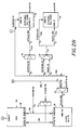
- a Central Processor (CP) 12 is coupled to an 8K by 88-bit Control Store 14 by a 14-bit control store address bus 14a and an 88-bit control store data bus 14b.
- the Control Store 14 stores microinstructions (micro-code) which are read into the CP 12 in order to execute macroinstructions that are read from an 8K by 72-bit CACHE memory 16, via a CACHE Data Unit (CDU) 18, bidirectional 64-bit data bus BDS00:63 18a, and bidirectional 32-bit data bus DB00:32 12a.
- microinstructions micro-code
- CDU CACHE Data Unit
- Macroinstructions are fetched from the CACHE memory 16 in accordance with physical addresses provided by the CP 12 on a 32-bit physical address bus (PA0:31) 12b, via a CACHE address multiplexer (MUX) 20.
- the CACHE address MUX 20 is employed when pre-filling the CACHE 16 with instructions and data.
- PA bits 16:28 are provided to the CACHE 20.
- PA bit 28 being provided as the LSB address bit enables a Double-Word (eight bytes or two 32-bit words) to be read by the CP 12 over the 64-bit bus 18a and 32-bit bus 12a.
- the eight bit DSPO:7 bus 18b conveys data parity bits between the CACHE 16 and the CDU 18.
- the CDU 18 operates as a data buffer for interfacing the 32-bit CP 12 data bus 12a to the 64-bit cache/main memory data bus 18a, as a data error checker, and provides data alignment for the CP 12.
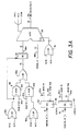
- the CDU 18 receives a sub-set of the Control Store 14 output bits (CS) and includes the logic that provides the hardware-assisted MCOUNT instruction of this invention, as will be described in detail below with respect to FIG. 3A.
- the macroinstructions that are read from the CACHE 16 are those that implement the VS Assembly Language program that is provided by Wang Laboratories Inc. of Lowell MA.
- One of the macroinstructions is referred to as the Modify Count (MCOUNT) instruction that was briefly described above.
- MCOUNT Modify Count
- a presently preferred technique for providing a hardware assist for the MCOUNT instruction is described in detail below.
- the 32-bit processor data bus 12a is buffered by a transceiver 22 and is provided as a buffered data bus (BDB0:31) 22a to several locations, including a 16K by 8-bit Data Key memory 24, a 16-bit control and status register (XCTLREG) 26, a reference and change table (REF/CHG TABLE) 28, and a system (backplane) Bus Interface Chip (BIC) 30.
- BDB0:31 buffered data bus
- XCTLREG 16-bit control and status register
- REF/CHG TABLE reference and change table
- BIC system (backplane) Bus Interface Chip
- the Data Key memory 24 stores encrypted information and provides a capability to enable only specified software packages to be executed by the CP 12.
- the REF/CHG Table 28 functions to indicate a reference to a particular page of memory, and to indicate if the reference was a write operation.
- the BIC 30 provides an interface to other components that are coupled to the system bus 32, the system bus including a 32-bit multiplexed address/data bus (AD31:0) 32a, associated parity lines (PAR3:0) 32b, and control signal lines 32c. In general, the BIC 30 operates to arbitrate access to the system bus 32 and to perform all necessary handshaking with other devices that are coupled to the system bus 32.
- a memory control function is also contained within the BIC 30.
- the XCTLREG 26 enables control over the CACHE memory 16, indicates CACHE status, and also provides indications of correctable and uncorrectable data errors.
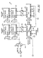
- a buffer 34 drives the PA bus 12b as a CP Address (CPA) bus 34a to the Data Key 24 (14 bits), the REF/CHG Table 28 (16 bits) and a Memory Address Unit (MAU) 36 (27 bits).
- the MAU 36 operates to queue memory read and write addresses and functions, in conjunction with even and odd Memory Data Units (MDUs) 38a and 38b, respectively, to write and read data from main memory 40.
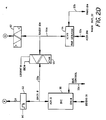
- Main memory 40 is comprised of a plurality of DRAM modules 40a-40d, and is organized as an even word array (modules 40a and 40b) and as an odd word array (modules 40c and 40d).
- the total width of the main memory 40 is 64 bits (a double word), plus 14 bits of ECC parity information. ECC is performed separately on each odd and even 32-bit memory word.
- the MAU 36 also receives a 27-bit I/O address (IOA) bus 36a that is sourced from the BIC 30 via a Buffered Address (BA) bus 30a and a latch 42.
- IOA bus 36a provides a first memory address of a data block that is to be written to or read from by an I/O device that is coupled to the system bus 32. The first address is received though a transceiver 44, a buffered address/data (BAD) bus 44a, and a transceiver 45.
- Transceiver 45 is enabled to pass the first memory address of the memory block to the BIC 30 and the latch 42, via the BA bus 30a.
- the first address is buffered, and subsequent memory addresses are incremented by the BIC 30 during an I/O operation and provided over the buses 30a and 36a, via latch 42. This enables a potentially large number of reads or writes to be made to consecutive memory locations of the main memory 40.
- One output of the MAU 36 is a 22-bit memory address (MA) bus 36b that is applied to a row/column MUX 46 which has a 12-bit output for sequentially providing row and column addresses, via drivers 48a-48d, to the DRAM modules 40a-40d, respectively.
- the row/column MUX 46 operates under the control of a COL signal that is generated by a memory control state machine (not shown).
- UPDT 24-bit update address
- XMAR 50 sources a registered update address (RUPDT) bus 50a to the MUX 20 (13 bits), to a MUX 52 (24 bits), to a driver 54, and to an External Tag Store 56.
- RPDT registered update address
- MUX 52 Also provided to MUX 52 is the PA bus 12b.
- the output of the MUX 52 is a 13-bit internal tag store address (ITSA) bus 52a and an 11-bit internal tag store data (ITSD) bus 52b which are applied to an Internal Tag Store 58.
- ITSA 13-bit internal tag store address
- ITSD 11-bit internal tag store data
- the output of the driver 54 is a 13-bit external tag store address (XTSA) bus 54a which is applied to the External Tag Store 56, in conjunction with 11-bits of the RUPDT bus 50a.
- the External Tag Store 56 and the Internal Tag Store 58 provide CACHE hit and miss detection, XMIS and IMIS, respectively, for I/O accesses and CP 12 accesses, respectively.
- the MDUs 38a and 38b operate in conjunction with registered buffers 60a and 60b, respectively, to provide a data queue for read and write accesses of the main memory 40.
- the MDUs 38a and 38b also each provide for word-wide ECC generation and checking functions for data going to and coming from the main memory 40.
- Each of the MDUs 38a and 38b is bidirectionally coupled to one word (32-bits) of the 64-bit buffered data bus 18a, and thereby to the CACHE 16 and to the CDU 18.
- Each of the MDUs 38a and 38b also source 4-bits of the 8-bit CP Data Parity (CPDP) bus which is provided through a buffer 64 to the eight bit DSP0:7 bus 18b that conveys data parity bits between the CACHE 16 and the CDU 18.
- the MDUs 38a and 38b each also have a 32-bit I/O data path (IOD) and are bidirectionally coupled in parallel to a transceiver 62 and thence to the BAD bus 44a. For I/O data transfers to or from the system bus 32 the MDUs are alternately selected to either transmit up to a 32-bit word to the transceiver 62 or receive up to a 32-bit word from the transceiver 62.
- IOD I/O data path
- the data processor 10 of Figs. 2A-2D in a presently preferred embodiment of the invention, is packaged on a single multi-layered printed circuit board.
- the CDU 18, MAU 36, the MDUs 38a and 38b, and the BIC 30 are each contained within an Application Specific Integrated Circuit (ASIC).
- a CP 12 cycle is a minimum of 50 nanoseconds in duration (20 MHz clock frequency), and is comprised of two or more 50% duty cycle 25 nanosecond sub-cycles or "ticks".
- the CP 12 clock is synchronized to a 50 nanosecond clock signal that is provided on the system bus 32.
- This logic is preferably embodied external to the CP 12, within the CDU 18, and is shown in FIG 3A.
- R1 is a general CP 12 register into which the main memory word addressed by the second operand D2(X2,B2) is copied after being modified by addition or subtraction.
- the second operand addresses a target word in main memory 40 which is fullword aligned.
- M3 is a 16-bit function mask that determines the operation performed by MCOUNT.
- M4 is a 16-bit unsigned integer used as an increment for add immediate and subtract immediate functions, if specified by M3.
- M30 the most significant bit
- M31 the second MSB
- Table 2 the bits of interest in M3 are shown in Table 2.
- the resulting 2-bit Condition Code is defined as follows in Table 3. 0 Result is zero 1 Result is negative 2 Result is positive 3 Not defined
- the Specification Exception results from an illegal (undefined) M3 operand.
- the micro-code is stored within the Control Store 14 (Fig. 2A), and is read by the CP 12 on the occurrence of an MCOUNT instruction being received over the DB0:31 bus 12a from the CACHE 16 via the CDU 18.
- a sub-set of the microcode bits (CS) is input to the CDU 18, which then cooperates with the CP 12 to execute the MCOUNT instruction.
- a first portion of the micro-code employs a CP 12 Memory Address Register (MAR) to generate the address for the second word of the two word MCOUNT Instruction. If an index register is in use, then it is added to the effective address within the MAR.
- MAR Memory Address Register
- NOP (MAR2/RW) /LDM34/ XTS1, MCNTXCHG
- This micro-code instruction activates, via the CS bits, a Load Mask 3&4 (LDM34) control signal line 80 to load M3 from data bus signal lines 0:15 (DBDI0_15) into register M3 82, and to load M4 from data bus signal lines 16:31 (DBDI16_31) into register M4 84.
- Registers M3 82 and M4 84 each provide a 16-bit true bus (82a, 84a) and a 16-bit negated bus (82b, 84b).
- M3 82 During the execution of this first micro-code instruction the various outputs of M3 82 are applied to a combinatorial logic block which decodes M3. If M3 is equal to 8000, 4000, 1000, or 0800 no output is provided from the logic block. If M3 is equal to 2000, indicating an exchange between main memory and R1, then the signal M2000 is asserted. If M3 does not equal any of the defined M3 values of Table 1, then the ERR2000 signal is asserted. The logic block that decodes M3 is not shown. The M2000 and ERR2000 signals are applied as External Status inputs (XTS1) to the CP 12, and are checked at the completion of the first micro-instruction.
- XTS1 External Status inputs
- MCOUNT Exchange (MCNTXCHG) where, if M2000 is asserted, a read word from memory operation is performed, the memory word is placed in the general CP 12 register, and the content of the general register is written back out to main memory 40, thereby accomplishing the exchange operation.
- micro-code execution continues at instruction (2):
- This micro-code instruction reads the word to be modified from memory, stores the word in a CP 12 file register (FR2), and applies the word to a first input of an adder (ADD) 88 on a 32-bit bus 88a (RRB0_31).
- a second input (88b) of the adder 88 is supplied with the content of M4 84 if M3 is equal to 1000 or 0800 (see Tables 1 and 2). This is accomplished through the combinatorial logic block 90 and the sign extend (SE) block 92.
- the SE block 92 inputs a 16-bit half-word and outputs a sign-extended 32-bit word to the second input of the adder 88.
- M3 bit 1 or M3 bit 4 asserted If a subtraction operation is indicated by the output of 2OR 90a (M3 bit 1 or M3 bit 4 asserted), then a 1 is sign extended through bits 00:15, otherwise these bits are made zero, and the inversion of M4 (M40:15*) is gated through the AND gate 90c of block 90. If M3 bit 1 is asserted (indicating that M4 is not used for the increment) then M40:15 are also gated through the AND gate 90d, resulting in all ones being output from the OR gate 90e and applied to SE 92. If M3 bit 4 is asserted, then the inversion of M4 is gated through AND gate 90c and OR gate 90e to the input of SE 92.
- a Carry-In (CI) input of the adder 88 is set for the case where either M3 bit 0 or M3 bit 4 are asserted, via the OR gate 94.
- the result of this gating scheme is the control of the operands and CI input of the adder 88 to accomplish the action dictated by the state of M3 bits 0, 1, 3, or 4, as indicated in Tables 1 and 2.
- the result of the addition or subtraction is provided during the execution of the second micro-code instruction on the 32-bit result bus 88c (MCOUT0_31).
- the adder 88 also provides three status outputs indicating an overflow (OVFL), a zero result (ALU), and a sign (SIGN) of the output appearing on MCOUT0_31. These status outputs are provided as inputs to a combinatorial logic block which generates the 2-bit condition code (MXCC) therefrom, as indicated in Table 3. It is noted that the OVFL bit being asserted results in a condition code indication of 3. However, the OVFL condition also causes the CP exception referred to above, with a branch being taken to PCHKBOVF. As such, the actual state of the condition code is not checked, and is defined in Table 3 to be undefined. The logic block that decodes the status outputs is not shown.
- MXCC 2-bit condition code
- the third micro-code instruction is executed.
- the output word of the adder is written back to main memory, the CP register is updated with the result of the adder 88, thereby accomplishing atomic read-modify-write operation that is implemented by the MCOUNT instruction.
- the overall execution time of the RMW operation is increased significantly, thereby improving the overall operating speed of the system 10 and reducing the amount of time that the memory is locked and not available to other memory requestors.
Landscapes
- Engineering & Computer Science (AREA)
- Software Systems (AREA)
- Theoretical Computer Science (AREA)
- Physics & Mathematics (AREA)
- General Physics & Mathematics (AREA)
- General Engineering & Computer Science (AREA)
- Computational Mathematics (AREA)
- Mathematical Analysis (AREA)
- Mathematical Optimization (AREA)
- Pure & Applied Mathematics (AREA)
- Advance Control (AREA)
- Memory System Of A Hierarchy Structure (AREA)
- Executing Machine-Instructions (AREA)
Abstract
Claims (13)
- Procédé pour exécuter une opération de mémoire du type lecture - modification - écriture arithmétique par un processeur de données (10) qui est couplé à une mémoire (40) possédant des emplacements de mémoire, l'opération de mémoire du type lecture - modification - écriture arithmétique étant exécutée sur une pluralité d'intervalles de temps consécutifs associés à l'exécution de micro-instructions, caractérisé par les étapes consistant à :pendant un premier intervalle de temps:charger un premier registre (82) avec des premières données de masque (M3) qui indiquent une opération à exécuter sur des données de cible situées dans un emplacement de mémoire, les premières données de masque indiquant des opérations qui comprennent : l'incrémentation de données de cible; la décrémentation de données de cible; l'incrémentation de données de cible d'une quantité indiquée par les deuxièmes données de masque; la décrémentation de données de cible d'une quantité indiquée par les deuxièmes données de masque; et l'échange de données de cible avec des données enregistrées dans un registre du processeur de données;charger un deuxième registre (84) avec des deuxièmes données de masque (M4) qui indiquent les données qui peuvent être ajoutées aux ou soustraites des données de cible situées dans l'emplacement de mémoire; etappliquer les premières données de masque à un moyen de logique (90) et décoder l'opération à exécuter;pendant un deuxième intervalle de temps,lire les données de cible;en réponse à un résultat du moyen de logique, exécuter l'opération indiquée en appliquant les données de cible à un moyen de circuit (88) et en faisant opérer le moyen de circuit pour exécuter l'opération indiquée; etpendant un troisième intervalle de temps,enregistrer un résultat de l'opération indiquée (MCOUTO_31) dans un registre (R1) du processeur de données et également dans l'emplacement de mémoire.
- Procédé selon la revendication 1 dans lequel chacun des intervalles de temps correspond à l'exécution d'une micro-instruction.
- Procédé selon la revendication 1 dans lequel l'étape consistant à décoder comprend une étape consistant à détecter que les premières données de masque n'indiquent pas une opération valide, et une étape consistant à générer un état d'exception à notifier au processeur de données.
- Procédé selon la revendication 1 dans lequel l'étape consistant à exécuter l'opération indiquée comprend une étape consistant à générer une pluralité de codes de condition (ALU, SIGN), et une étape consistant à appliquer les codes de condition au processeur de données.
- Procédé selon la revendication 4 dans lequel les codes de condition comprennent un code de condition (SIGN) qui indique un signe du résultat, et un code de condition (ALU) qui indique si le résultat est zéro.
- Procédé selon la revendication 1 dans lequel l'étape consistant à exécuter l'opération indiquée comprend une étape consistant à générer un état d'exception (OVFL) pour indiquer que l'exécution de l'opération indiquée a eu comme conséquence un état de dépassement de capacité.
- Dispositif pour exécuter une opération de mémoire du type lecture - modification - écriture arithmétique par un processeur de données (10) qui est couplé à une mémoire (40) ayant des emplacements de mémoire, l'opération de mémoire du type lecture - modification - écriture arithmétique étant exécutée sur une pluralité d'intervalles de temps consécutifs associés à l'exécution de micro-instructions, caractérisé par :un premier registre (82) pour enregistrer, pendant un premier intervalle de temps, des premières données de masque (M3) qui indiquent une opération à exécuter sur des données de cible situées dans un emplacement de mémoire, les premières données de masque indiquant des opérations qui comprennent : l'incrémentation des données de cible; la décrémentation des données de cible; l'incrémentation des données de cible d'une quantité indiquée par des deuxièmes données de masque; la décrémentation des données de cible d'une quantité indiquée par les deuxièmes données de masque; et l'échange des données de cible avec des données enregistrées dans un registre du processeur de données;un deuxième registre (84) pour enregistrer, pendant le premier intervalle de temps, des deuxièmes données de masque (M4) qui indiquent des données qui peuvent être ajoutées aux ou soustraites des données de cible situées dans l'emplacement de mémoire;un moyen de logique (90), fonctionnant pendant le premier intervalle de temps, pour décoder les premières données de masque pour déterminer l'opération à exécuter;un moyen pour lire (18) les données de cible pendant un deuxième intervalle de temps;un moyen sensible à une sortie du moyen de logique, pour exécuter (88) l'opération indiquée sur les données de cible pendant le deuxième intervalle; etun moyen pour enregistrer (18) un résultat de l'opération indiquée (MCOUTO_31) dans un registre (R1) du processeur de données et également dans l'emplacement de mémoire.
- Dispositif selon la revendication 1 dans lequel chacun des intervalles de temps correspond à l'exécution d'une micro-instruction.
- Dispositif selon la revendication 7 dans lequel le moyen pour décoder comprend un moyen pour détecter que les premières données de masque n'indiquent pas une opération valide, et un moyen pour générer un état d'exception à notifier au processeur de données.
- Dispositif selon la revendication 7 dans lequel le moyen pour exécuter comprend un moyen pour générer une pluralité de codes de condition (ALU, SIGN) comme résultat de l'exécution de l'opération.
- Dispositif selon la revendication 10 dans lequel les codes de condition comprennent un code de condition (SIGN) qui indique un signe du résultat, et un code de condition (ALU) qui indique si le résultat est zéro.
- Dispositif selon la revendication 7 dans lequel le moyen pour exécuter comprend un moyen pour générer un état d'exception (OVFL) pour indiquer que l'exécution de l'opération indiquée a eu comme conséquence un état de dépassement de capacité.
- Dispositif selon la revendication 7 dans lequel lesdits premier et deuxième moyens de registre, ledit moyen logique et ledit moyen pour exécuter sont tous situés à l'extérieur du processeur de données.
Applications Claiming Priority (3)
| Application Number | Priority Date | Filing Date | Title |
|---|---|---|---|
| US13510993A | 1993-10-12 | 1993-10-12 | |
| US135109 | 1993-10-12 | ||
| PCT/US1994/003219 WO1995010804A1 (fr) | 1993-10-12 | 1994-03-24 | Execution d'une instruction de modification de comptage assistee par circuit specialise |
Publications (2)
| Publication Number | Publication Date |
|---|---|
| EP0723680A1 EP0723680A1 (fr) | 1996-07-31 |
| EP0723680B1 true EP0723680B1 (fr) | 1998-08-12 |
Family
ID=22466599
Family Applications (1)
| Application Number | Title | Priority Date | Filing Date |
|---|---|---|---|
| EP94919077A Expired - Lifetime EP0723680B1 (fr) | 1993-10-12 | 1994-03-24 | Execution d'une instruction de modification de comptage assistee par circuit specialise |
Country Status (6)
| Country | Link |
|---|---|
| US (1) | US5542084A (fr) |
| EP (1) | EP0723680B1 (fr) |
| AU (1) | AU677673B2 (fr) |
| CA (1) | CA2173226C (fr) |
| DE (1) | DE69412504T2 (fr) |
| WO (1) | WO1995010804A1 (fr) |
Families Citing this family (21)
| Publication number | Priority date | Publication date | Assignee | Title |
|---|---|---|---|---|
| US5546343A (en) * | 1990-10-18 | 1996-08-13 | Elliott; Duncan G. | Method and apparatus for a single instruction operating multiple processors on a memory chip |
| US5838960A (en) * | 1996-09-26 | 1998-11-17 | Bay Networks, Inc. | Apparatus for performing an atomic add instructions |
| KR100284904B1 (ko) * | 1998-05-29 | 2001-05-02 | 윤종용 | 불 휘발성 반도체 메모리 장치 및 그 장치의 무효 메모리 블록데이블 세팅 방법 |
| US6986025B2 (en) * | 2001-06-11 | 2006-01-10 | Broadcom Corporation | Conditional execution per lane |
| US7861071B2 (en) * | 2001-06-11 | 2010-12-28 | Broadcom Corporation | Conditional branch instruction capable of testing a plurality of indicators in a predicate register |
| US7127593B2 (en) * | 2001-06-11 | 2006-10-24 | Broadcom Corporation | Conditional execution with multiple destination stores |
| US7017032B2 (en) * | 2001-06-11 | 2006-03-21 | Broadcom Corporation | Setting execution conditions |
| US7415601B2 (en) * | 2002-06-28 | 2008-08-19 | Motorola, Inc. | Method and apparatus for elimination of prolog and epilog instructions in a vector processor using data validity tags and sink counters |
| CN100595731C (zh) * | 2003-03-21 | 2010-03-24 | 凌阳科技股份有限公司 | 利用同位检查以进行指令模式切换的处理器及方法 |
| US7475393B2 (en) * | 2003-08-29 | 2009-01-06 | Motorola, Inc. | Method and apparatus for parallel computations with incomplete input operands |
| US7290122B2 (en) * | 2003-08-29 | 2007-10-30 | Motorola, Inc. | Dataflow graph compression for power reduction in a vector processor |
| CN101258477B (zh) * | 2004-10-25 | 2010-10-06 | 集成装置技术公司 | 统计引擎 |
| CN100367192C (zh) * | 2005-03-01 | 2008-02-06 | 华晶科技股份有限公司 | 具有一微码引擎的中央处理单元 |
| US8069340B2 (en) * | 2008-02-08 | 2011-11-29 | Via Technologies, Inc. | Microprocessor with microarchitecture for efficiently executing read/modify/write memory operand instructions |
| US7945768B2 (en) * | 2008-06-05 | 2011-05-17 | Motorola Mobility, Inc. | Method and apparatus for nested instruction looping using implicit predicates |
| US8843729B2 (en) | 2010-04-27 | 2014-09-23 | Via Technologies, Inc. | Microprocessor that fuses MOV/ALU instructions |
| US8856496B2 (en) | 2010-04-27 | 2014-10-07 | Via Technologies, Inc. | Microprocessor that fuses load-alu-store and JCC macroinstructions |
| US9483266B2 (en) | 2013-03-15 | 2016-11-01 | Intel Corporation | Fusible instructions and logic to provide OR-test and AND-test functionality using multiple test sources |
| US9886277B2 (en) | 2013-03-15 | 2018-02-06 | Intel Corporation | Methods and apparatus for fusing instructions to provide OR-test and AND-test functionality on multiple test sources |
| GB2533568B (en) | 2014-12-19 | 2021-11-17 | Advanced Risc Mach Ltd | Atomic instruction |
| US11989555B2 (en) * | 2017-06-29 | 2024-05-21 | Intel Corporation | Instructions for remote atomic operations |
Family Cites Families (10)
| Publication number | Priority date | Publication date | Assignee | Title |
|---|---|---|---|---|
| US3430209A (en) * | 1966-11-25 | 1969-02-25 | Gen Electric | Memory utilization apparatus and method |
| US3982229A (en) * | 1975-01-08 | 1976-09-21 | Bell Telephone Laboratories, Incorporated | Combinational logic arrangement |
| US4761755A (en) * | 1984-07-11 | 1988-08-02 | Prime Computer, Inc. | Data processing system and method having an improved arithmetic unit |
| US4896259A (en) * | 1984-09-07 | 1990-01-23 | International Business Machines Corporation | Apparatus for storing modifying data prior to selectively storing data to be modified into a register |
| JPS6167156A (ja) * | 1984-09-07 | 1986-04-07 | インタ−ナショナル ビジネス マシ−ンズ コ−ポレ−ション | デ−タ読取り/変更装置 |
| JPS61104391A (ja) * | 1984-10-23 | 1986-05-22 | Fujitsu Ltd | 半導体記憶装置 |
| US4884271A (en) * | 1987-12-28 | 1989-11-28 | International Business Machines Corporation | Error checking and correcting for read-modified-write operations |
| US5235693A (en) * | 1989-01-27 | 1993-08-10 | Digital Equipment Corporation | Method and apparatus for reducing buffer storage in a read-modify-write operation |
| JP3038781B2 (ja) * | 1989-04-21 | 2000-05-08 | 日本電気株式会社 | メモリアクセス制御回路 |
| US5167029A (en) * | 1989-12-13 | 1992-11-24 | International Business Machines Corporation | Data processing system and associated process using memory cards having data modify functions utilizing a data mask and an internal register |
-
1994
- 1994-03-24 AU AU70140/94A patent/AU677673B2/en not_active Expired
- 1994-03-24 WO PCT/US1994/003219 patent/WO1995010804A1/fr not_active Ceased
- 1994-03-24 DE DE69412504T patent/DE69412504T2/de not_active Expired - Lifetime
- 1994-03-24 EP EP94919077A patent/EP0723680B1/fr not_active Expired - Lifetime
- 1994-03-24 CA CA002173226A patent/CA2173226C/fr not_active Expired - Lifetime
- 1994-11-22 US US08/343,268 patent/US5542084A/en not_active Expired - Lifetime
Also Published As
| Publication number | Publication date |
|---|---|
| CA2173226C (fr) | 2001-08-14 |
| AU7014094A (en) | 1995-05-04 |
| EP0723680A1 (fr) | 1996-07-31 |
| CA2173226A1 (fr) | 1995-04-20 |
| DE69412504D1 (de) | 1998-09-17 |
| DE69412504T2 (de) | 1999-03-25 |
| AU677673B2 (en) | 1997-05-01 |
| WO1995010804A1 (fr) | 1995-04-20 |
| US5542084A (en) | 1996-07-30 |
Similar Documents
| Publication | Publication Date | Title |
|---|---|---|
| US5542084A (en) | Method and apparatus for executing an atomic read-modify-write instruction | |
| US5481734A (en) | Data processor having 2n bits width data bus for context switching function | |
| US5367705A (en) | In-register data manipulation using data shift in reduced instruction set processor | |
| US5454091A (en) | Virtual to physical address translation scheme with granularity hint for identifying subsequent pages to be accessed | |
| JP2796590B2 (ja) | メモリ装置及びそれを使用したデータ処理装置 | |
| EP0465321B1 (fr) | Assurer l'intégrité de données dans un système à processeur multiple ou en pipeline | |
| EP0463975B1 (fr) | Fonction de comparaison d'octets pour un processeur à haute performance | |
| US6076158A (en) | Branch prediction in high-performance processor | |
| US6167509A (en) | Branch performance in high speed processor | |
| US5778423A (en) | Prefetch instruction for improving performance in reduced instruction set processor | |
| US5142631A (en) | System for queuing individual read or write mask and generating respective composite mask for controlling access to general purpose register | |
| US8627471B2 (en) | Permissions checking for data processing instructions | |
| US9213665B2 (en) | Data processor for processing a decorated storage notify | |
| US5502827A (en) | Pipelined data processor for floating point and integer operation with exception handling | |
| US5469551A (en) | Method and apparatus for eliminating branches using conditional move instructions | |
| US5668967A (en) | Apparatus and methods for reducing numbers of read-modify-write cycles to a memory, and for improving DMA efficiency | |
| US6363474B1 (en) | Process switching register replication in a data processing system | |
| US5564030A (en) | Circuit and method for detecting segment limit errors for code fetches | |
| GB2200481A (en) | Maintaining coherence between a microprocessor's integrated cache and external memory | |
| US6757809B1 (en) | Data processor having 2n bits width data bus for context switching functions | |
| JPH04275627A (ja) | 中央演算処理装置 | |
| IE901524A1 (en) | Control of multiple function units with parallel operation¹in a microcoded execution unit |
Legal Events
| Date | Code | Title | Description |
|---|---|---|---|
| PUAI | Public reference made under article 153(3) epc to a published international application that has entered the european phase |
Free format text: ORIGINAL CODE: 0009012 |
|
| 17P | Request for examination filed |
Effective date: 19960402 |
|
| AK | Designated contracting states |
Kind code of ref document: A1 Designated state(s): DE FR GB |
|
| GRAG | Despatch of communication of intention to grant |
Free format text: ORIGINAL CODE: EPIDOS AGRA |
|
| 17Q | First examination report despatched |
Effective date: 19971103 |
|
| RAP1 | Party data changed (applicant data changed or rights of an application transferred) |
Owner name: SAMSUNG ELECTRONICS CO., LTD. |
|
| GRAG | Despatch of communication of intention to grant |
Free format text: ORIGINAL CODE: EPIDOS AGRA |
|
| GRAH | Despatch of communication of intention to grant a patent |
Free format text: ORIGINAL CODE: EPIDOS IGRA |
|
| GRAH | Despatch of communication of intention to grant a patent |
Free format text: ORIGINAL CODE: EPIDOS IGRA |
|
| GRAA | (expected) grant |
Free format text: ORIGINAL CODE: 0009210 |
|
| AK | Designated contracting states |
Kind code of ref document: B1 Designated state(s): DE FR GB |
|
| REF | Corresponds to: |
Ref document number: 69412504 Country of ref document: DE Date of ref document: 19980917 |
|
| ET | Fr: translation filed | ||
| PLBE | No opposition filed within time limit |
Free format text: ORIGINAL CODE: 0009261 |
|
| STAA | Information on the status of an ep patent application or granted ep patent |
Free format text: STATUS: NO OPPOSITION FILED WITHIN TIME LIMIT |
|
| 26N | No opposition filed | ||
| REG | Reference to a national code |
Ref country code: GB Ref legal event code: IF02 |
|
| PGFP | Annual fee paid to national office [announced via postgrant information from national office to epo] |
Ref country code: GB Payment date: 20130304 Year of fee payment: 20 Ref country code: DE Payment date: 20130305 Year of fee payment: 20 Ref country code: FR Payment date: 20130402 Year of fee payment: 20 |
|
| REG | Reference to a national code |
Ref country code: DE Ref legal event code: R071 Ref document number: 69412504 Country of ref document: DE |
|
| REG | Reference to a national code |
Ref country code: DE Ref legal event code: R071 Ref document number: 69412504 Country of ref document: DE |
|
| REG | Reference to a national code |
Ref country code: GB Ref legal event code: PE20 Expiry date: 20140323 |
|
| PG25 | Lapsed in a contracting state [announced via postgrant information from national office to epo] |
Ref country code: DE Free format text: LAPSE BECAUSE OF EXPIRATION OF PROTECTION Effective date: 20140325 Ref country code: GB Free format text: LAPSE BECAUSE OF EXPIRATION OF PROTECTION Effective date: 20140323 |