EP0724183A2 - Flussigkristall-Anzeige und Verfahren zu ihrer Herstellung - Google Patents
Flussigkristall-Anzeige und Verfahren zu ihrer Herstellung Download PDFInfo
- Publication number
- EP0724183A2 EP0724183A2 EP96100908A EP96100908A EP0724183A2 EP 0724183 A2 EP0724183 A2 EP 0724183A2 EP 96100908 A EP96100908 A EP 96100908A EP 96100908 A EP96100908 A EP 96100908A EP 0724183 A2 EP0724183 A2 EP 0724183A2
- Authority
- EP
- European Patent Office
- Prior art keywords
- film
- liquid crystal
- substrate
- crystal display
- wirings
- Prior art date
- Legal status (The legal status is an assumption and is not a legal conclusion. Google has not performed a legal analysis and makes no representation as to the accuracy of the status listed.)
- Granted
Links
- 239000004973 liquid crystal related substance Substances 0.000 title claims abstract description 35
- 238000004519 manufacturing process Methods 0.000 title claims description 6
- 239000010408 film Substances 0.000 claims abstract description 147
- 239000000758 substrate Substances 0.000 claims abstract description 60
- 239000010409 thin film Substances 0.000 claims abstract description 9
- 239000011159 matrix material Substances 0.000 claims abstract description 6
- 230000001681 protective effect Effects 0.000 claims description 27
- 239000004065 semiconductor Substances 0.000 claims description 22
- 238000000059 patterning Methods 0.000 claims description 13
- 239000000463 material Substances 0.000 claims description 11
- 229920002120 photoresistant polymer Polymers 0.000 claims description 9
- 229910021417 amorphous silicon Inorganic materials 0.000 claims description 6
- 229910052782 aluminium Inorganic materials 0.000 claims description 3
- 229910052804 chromium Inorganic materials 0.000 claims description 3
- 229910052715 tantalum Inorganic materials 0.000 claims description 3
- 239000013078 crystal Substances 0.000 claims description 2
- 229910052742 iron Inorganic materials 0.000 claims description 2
- 229910052750 molybdenum Inorganic materials 0.000 claims description 2
- 229910052759 nickel Inorganic materials 0.000 claims description 2
- 229910052758 niobium Inorganic materials 0.000 claims description 2
- 229910052719 titanium Inorganic materials 0.000 claims description 2
- 229910052721 tungsten Inorganic materials 0.000 claims description 2
- XUIMIQQOPSSXEZ-UHFFFAOYSA-N Silicon Chemical compound [Si] XUIMIQQOPSSXEZ-UHFFFAOYSA-N 0.000 claims 1
- 229910052710 silicon Inorganic materials 0.000 claims 1
- 239000010703 silicon Substances 0.000 claims 1
- 238000000034 method Methods 0.000 abstract description 54
- 238000005268 plasma chemical vapour deposition Methods 0.000 description 8
- 238000001312 dry etching Methods 0.000 description 7
- 238000005530 etching Methods 0.000 description 7
- 230000002093 peripheral effect Effects 0.000 description 7
- 229910052581 Si3N4 Inorganic materials 0.000 description 6
- HQVNEWCFYHHQES-UHFFFAOYSA-N silicon nitride Chemical compound N12[Si]34N5[Si]62N3[Si]51N64 HQVNEWCFYHHQES-UHFFFAOYSA-N 0.000 description 6
- 238000001755 magnetron sputter deposition Methods 0.000 description 4
- 238000004544 sputter deposition Methods 0.000 description 4
- XLYOFNOQVPJJNP-UHFFFAOYSA-N water Substances O XLYOFNOQVPJJNP-UHFFFAOYSA-N 0.000 description 4
- QTBSBXVTEAMEQO-UHFFFAOYSA-N Acetic acid Chemical compound CC(O)=O QTBSBXVTEAMEQO-UHFFFAOYSA-N 0.000 description 3
- GRYLNZFGIOXLOG-UHFFFAOYSA-N Nitric acid Chemical compound O[N+]([O-])=O GRYLNZFGIOXLOG-UHFFFAOYSA-N 0.000 description 3
- BLRPTPMANUNPDV-UHFFFAOYSA-N Silane Chemical compound [SiH4] BLRPTPMANUNPDV-UHFFFAOYSA-N 0.000 description 3
- 230000015572 biosynthetic process Effects 0.000 description 3
- 238000000151 deposition Methods 0.000 description 3
- 229910017604 nitric acid Inorganic materials 0.000 description 3
- 238000000206 photolithography Methods 0.000 description 3
- 229920001721 polyimide Polymers 0.000 description 3
- NBIIXXVUZAFLBC-UHFFFAOYSA-N Phosphoric acid Chemical compound OP(O)(O)=O NBIIXXVUZAFLBC-UHFFFAOYSA-N 0.000 description 2
- 239000004642 Polyimide Substances 0.000 description 2
- 230000003247 decreasing effect Effects 0.000 description 2
- 239000007788 liquid Substances 0.000 description 2
- 238000009832 plasma treatment Methods 0.000 description 2
- HXVNBWAKAOHACI-UHFFFAOYSA-N 2,4-dimethyl-3-pentanone Chemical compound CC(C)C(=O)C(C)C HXVNBWAKAOHACI-UHFFFAOYSA-N 0.000 description 1
- 229910004014 SiF4 Inorganic materials 0.000 description 1
- DAKKHQAZXRANTD-UHFFFAOYSA-O [NH4+].[Ce+2].[O-][N+]([O-])=O.[O-][N+]([O-])=O.[O-][N+]([O-])=O Chemical compound [NH4+].[Ce+2].[O-][N+]([O-])=O.[O-][N+]([O-])=O.[O-][N+]([O-])=O DAKKHQAZXRANTD-UHFFFAOYSA-O 0.000 description 1
- 229910000147 aluminium phosphate Inorganic materials 0.000 description 1
- 238000005516 engineering process Methods 0.000 description 1
- 238000010438 heat treatment Methods 0.000 description 1
- 238000010030 laminating Methods 0.000 description 1
- 238000005259 measurement Methods 0.000 description 1
- 229910052751 metal Inorganic materials 0.000 description 1
- 239000002184 metal Substances 0.000 description 1
- 239000007769 metal material Substances 0.000 description 1
- 229910021424 microcrystalline silicon Inorganic materials 0.000 description 1
- 239000000203 mixture Substances 0.000 description 1
- 229920003986 novolac Polymers 0.000 description 1
- 239000003960 organic solvent Substances 0.000 description 1
- KNCYXPMJDCCGSJ-UHFFFAOYSA-N piperidine-2,6-dione Chemical compound O=C1CCCC(=O)N1 KNCYXPMJDCCGSJ-UHFFFAOYSA-N 0.000 description 1
- 229920003229 poly(methyl methacrylate) Polymers 0.000 description 1
- 239000009719 polyimide resin Substances 0.000 description 1
- 239000004926 polymethyl methacrylate Substances 0.000 description 1
- 238000007789 sealing Methods 0.000 description 1
- ABTOQLMXBSRXSM-UHFFFAOYSA-N silicon tetrafluoride Chemical compound F[Si](F)(F)F ABTOQLMXBSRXSM-UHFFFAOYSA-N 0.000 description 1
- 239000002904 solvent Substances 0.000 description 1
- 239000011882 ultra-fine particle Substances 0.000 description 1
Images



Classifications
-
- G—PHYSICS
- G02—OPTICS
- G02F—OPTICAL DEVICES OR ARRANGEMENTS FOR THE CONTROL OF LIGHT BY MODIFICATION OF THE OPTICAL PROPERTIES OF THE MEDIA OF THE ELEMENTS INVOLVED THEREIN; NON-LINEAR OPTICS; FREQUENCY-CHANGING OF LIGHT; OPTICAL LOGIC ELEMENTS; OPTICAL ANALOGUE/DIGITAL CONVERTERS
- G02F1/00—Devices or arrangements for the control of the intensity, colour, phase, polarisation or direction of light arriving from an independent light source, e.g. switching, gating or modulating; Non-linear optics
- G02F1/01—Devices or arrangements for the control of the intensity, colour, phase, polarisation or direction of light arriving from an independent light source, e.g. switching, gating or modulating; Non-linear optics for the control of the intensity, phase, polarisation or colour
- G02F1/13—Devices or arrangements for the control of the intensity, colour, phase, polarisation or direction of light arriving from an independent light source, e.g. switching, gating or modulating; Non-linear optics for the control of the intensity, phase, polarisation or colour based on liquid crystals, e.g. single liquid crystal display cells
- G02F1/133—Constructional arrangements; Operation of liquid crystal cells; Circuit arrangements
- G02F1/1333—Constructional arrangements; Manufacturing methods
- G02F1/1345—Conductors connecting electrodes to cell terminals
- G02F1/13458—Terminal pads
-
- G—PHYSICS
- G02—OPTICS
- G02F—OPTICAL DEVICES OR ARRANGEMENTS FOR THE CONTROL OF LIGHT BY MODIFICATION OF THE OPTICAL PROPERTIES OF THE MEDIA OF THE ELEMENTS INVOLVED THEREIN; NON-LINEAR OPTICS; FREQUENCY-CHANGING OF LIGHT; OPTICAL LOGIC ELEMENTS; OPTICAL ANALOGUE/DIGITAL CONVERTERS
- G02F1/00—Devices or arrangements for the control of the intensity, colour, phase, polarisation or direction of light arriving from an independent light source, e.g. switching, gating or modulating; Non-linear optics
- G02F1/01—Devices or arrangements for the control of the intensity, colour, phase, polarisation or direction of light arriving from an independent light source, e.g. switching, gating or modulating; Non-linear optics for the control of the intensity, phase, polarisation or colour
- G02F1/13—Devices or arrangements for the control of the intensity, colour, phase, polarisation or direction of light arriving from an independent light source, e.g. switching, gating or modulating; Non-linear optics for the control of the intensity, phase, polarisation or colour based on liquid crystals, e.g. single liquid crystal display cells
- G02F1/133—Constructional arrangements; Operation of liquid crystal cells; Circuit arrangements
- G02F1/1333—Constructional arrangements; Manufacturing methods
- G02F1/1343—Electrodes
- G02F1/13439—Electrodes characterised by their electrical, optical, physical properties; materials therefor; method of making
-
- G—PHYSICS
- G02—OPTICS
- G02F—OPTICAL DEVICES OR ARRANGEMENTS FOR THE CONTROL OF LIGHT BY MODIFICATION OF THE OPTICAL PROPERTIES OF THE MEDIA OF THE ELEMENTS INVOLVED THEREIN; NON-LINEAR OPTICS; FREQUENCY-CHANGING OF LIGHT; OPTICAL LOGIC ELEMENTS; OPTICAL ANALOGUE/DIGITAL CONVERTERS
- G02F1/00—Devices or arrangements for the control of the intensity, colour, phase, polarisation or direction of light arriving from an independent light source, e.g. switching, gating or modulating; Non-linear optics
- G02F1/01—Devices or arrangements for the control of the intensity, colour, phase, polarisation or direction of light arriving from an independent light source, e.g. switching, gating or modulating; Non-linear optics for the control of the intensity, phase, polarisation or colour
- G02F1/13—Devices or arrangements for the control of the intensity, colour, phase, polarisation or direction of light arriving from an independent light source, e.g. switching, gating or modulating; Non-linear optics for the control of the intensity, phase, polarisation or colour based on liquid crystals, e.g. single liquid crystal display cells
- G02F1/133—Constructional arrangements; Operation of liquid crystal cells; Circuit arrangements
- G02F1/136—Liquid crystal cells structurally associated with a semi-conducting layer or substrate, e.g. cells forming part of an integrated circuit
- G02F1/1362—Active matrix addressed cells
-
- H—ELECTRICITY
- H10—SEMICONDUCTOR DEVICES; ELECTRIC SOLID-STATE DEVICES NOT OTHERWISE PROVIDED FOR
- H10D—INORGANIC ELECTRIC SEMICONDUCTOR DEVICES
- H10D30/00—Field-effect transistors [FET]
- H10D30/60—Insulated-gate field-effect transistors [IGFET]
- H10D30/67—Thin-film transistors [TFT]
-
- G—PHYSICS
- G02—OPTICS
- G02F—OPTICAL DEVICES OR ARRANGEMENTS FOR THE CONTROL OF LIGHT BY MODIFICATION OF THE OPTICAL PROPERTIES OF THE MEDIA OF THE ELEMENTS INVOLVED THEREIN; NON-LINEAR OPTICS; FREQUENCY-CHANGING OF LIGHT; OPTICAL LOGIC ELEMENTS; OPTICAL ANALOGUE/DIGITAL CONVERTERS
- G02F1/00—Devices or arrangements for the control of the intensity, colour, phase, polarisation or direction of light arriving from an independent light source, e.g. switching, gating or modulating; Non-linear optics
- G02F1/01—Devices or arrangements for the control of the intensity, colour, phase, polarisation or direction of light arriving from an independent light source, e.g. switching, gating or modulating; Non-linear optics for the control of the intensity, phase, polarisation or colour
- G02F1/13—Devices or arrangements for the control of the intensity, colour, phase, polarisation or direction of light arriving from an independent light source, e.g. switching, gating or modulating; Non-linear optics for the control of the intensity, phase, polarisation or colour based on liquid crystals, e.g. single liquid crystal display cells
- G02F1/133—Constructional arrangements; Operation of liquid crystal cells; Circuit arrangements
- G02F1/1333—Constructional arrangements; Manufacturing methods
- G02F1/1345—Conductors connecting electrodes to cell terminals
-
- G—PHYSICS
- G02—OPTICS
- G02F—OPTICAL DEVICES OR ARRANGEMENTS FOR THE CONTROL OF LIGHT BY MODIFICATION OF THE OPTICAL PROPERTIES OF THE MEDIA OF THE ELEMENTS INVOLVED THEREIN; NON-LINEAR OPTICS; FREQUENCY-CHANGING OF LIGHT; OPTICAL LOGIC ELEMENTS; OPTICAL ANALOGUE/DIGITAL CONVERTERS
- G02F1/00—Devices or arrangements for the control of the intensity, colour, phase, polarisation or direction of light arriving from an independent light source, e.g. switching, gating or modulating; Non-linear optics
- G02F1/01—Devices or arrangements for the control of the intensity, colour, phase, polarisation or direction of light arriving from an independent light source, e.g. switching, gating or modulating; Non-linear optics for the control of the intensity, phase, polarisation or colour
- G02F1/13—Devices or arrangements for the control of the intensity, colour, phase, polarisation or direction of light arriving from an independent light source, e.g. switching, gating or modulating; Non-linear optics for the control of the intensity, phase, polarisation or colour based on liquid crystals, e.g. single liquid crystal display cells
- G02F1/133—Constructional arrangements; Operation of liquid crystal cells; Circuit arrangements
- G02F1/136—Liquid crystal cells structurally associated with a semi-conducting layer or substrate, e.g. cells forming part of an integrated circuit
- G02F1/1362—Active matrix addressed cells
- G02F1/136286—Wiring, e.g. gate line, drain line
- G02F1/13629—Multilayer wirings
Definitions
- the present invention relates to an active matrix type liquid crystal display device driven by a thin film transistor (TFT) and a method of fabricating the same.
- TFT thin film transistor
- An object of the present invention is to provide a liquid crystal display device and a fabricating method of the same, whereby the fabricating processes are simplified, high product yield is provided, and an excellent picture displaying characteristic is obtained.
- a liquid crystal display device of the invention comprises a substrate having on the surface thereof a plurality of drain wirings, a plurality of gate wirings crossing the plurality of drain wirings in a matrix array, a plurality of thin film transistors disposed in the vicinity of each of the crossings, and a plurality of pixel electrodes connected to each of the thin film transistors, a substrate disposed in opposing relation to the above substrate, and a liquid crystal layer sandwiched between the above two substrates, in which metallic films of each of terminal portions of the plurality of drain wirings and the plurality of gate wirings are covered by transparent conductive films.
- a method of fabricating a liquid crystal display device of the invention comprises the step of forming source electrodes and drain wirings on a substrate, the step of forming a semiconductor film, an insulating film and a metallic film in succession over the above substrate, source electrodes and drain wirings, and then patterning these films using the same mask pattern to thereby form gate wirings, the step of forming a protective insulating film on the gate wirings and forming a photoresist on the same, the step of patterning the protective insulating film using the photoresist and then forming a transparent conductive film on the same, and the step of removing the transparent conductive film at the region where the photoresist pattern was formed to thereby form terminal portions of the source electrodes and the drain wirings as well as pixel electrodes.
- the materials of the drain and gate wirings in the liquid crystal display device of the invention Al, Cr, Mo, Ta, Ti, W, Nb, Fe, Co, Ni, and the like can be mentioned. It is also possible to deposit two kinds or more of these materials in layers. Further, as the material of the semiconductor layer, an Si film containing crystal phase, other than a-Si, may be used.
- the cross-sectional structures of the resist and the processed protective insulating film and gate insulating film become important factors affecting the processing accuracy of the transparent conductive film.
- the protective insulating film or the laminate of the protective insulating film and the gate insulating film is etched backwardly from the resist. This can be achieved by using such a material as silicon nitride (SiN) for the protective insulating film and the gate insulating film and performing dry etching using such a gas as SF 6 .
- the thickness of the protective insulating film or the total thickness of the protective insulating film and the gate insulating film is twice as large, or preferably three times as large, as the thickness of the transparent conductive film or above.
- a method can also be used in which two kinds of resists are laminated.
- a resist of the polyimide system for example, polyimide resin, polymethyl methacrylate, polymethyl glutarimide, and polymethyl isopropyl keton
- a resist of the novolak system may be used for the upper layer.
- the resist of the polyimide system is eroded by an alkaline developer and goes backward from the resist of the upper layer.
- the protective insulating film or the gate insulating film is processed by etching. At this time, backward etching is not particularly necessary. Thereafter, a transparent conductive film is formed and processing is made by the lift off method.
- crystalline ITO a material for the transparent electrode formed by adding Sn oxide to In oxide
- a resist with a low heat resistivity it may be practiced to form an amorphous ITO film at a lower temperature first and, then, after the resist has been removed, to crystallize ITO by heat treatment.
- a resist peeling liquid is used for peeling off the resist
- such a method may also be employed as to peel off the resist with a tape or to use a peeling liquid after the resist has been peeled off with a tape.
- the drain wiring, source electrodes, and pixel electrodes can be fabricated through one time of film depositing and photolithographic process.
- the thin film transistor layer, formed of a semiconductor layer and a gate insulating layer, and the gate wiring (gate electrode) layer through one and the same photolithographic process.
- the device through three photolithographic processes, i.e., the photolithographic process of the protective insulating film covering the whole surface of the device and having through holes for the pixel electrodes, in addition to the photolithographic process for the drain wiring, source electrodes and pixel electrodes and the photolithographic process for the thin film transistor layer and gate wiring.
- the photolithographic process of the protective insulating film covering the whole surface of the device and having through holes for the pixel electrodes in addition to the photolithographic process for the drain wiring, source electrodes and pixel electrodes and the photolithographic process for the thin film transistor layer and gate wiring.
- the liquid crystal driving circuit (mounted on a tape carrier package: TCP) and the gate-drain wiring on the substrate are generally connected by an anisotropic conductive film.
- ITO is being used for the drain wiring terminal and metal is being used for the gate wiring terminals.
- the reliability on the connection of the metallic terminal with the TCP was not sufficiently high.
- ITO is chemically stable, the reliability on the connection of it with the TCP is high. Therefore, the reliability on the device can be improved by covering the wiring terminals with ITO.
- the drain wiring is structured by using a metallic conductive film, the wiring resistance can be decreased. Hence, the potential gradient from the starting point to the terminal point of the drain wiring becomes gentle and the displaying characteristic of pixels such as uniformity of brightness can be improved.
- an ITO film is deposited on the resist pattern and it is subjected to patterning by the lift off method.
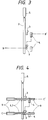
- Fig. 3 is a schematic plan view following the fabricating process of the substrate on the TFT side of the present invention and Fig. 6 is a schematic sectional view taken along line B-B' of Fig. 3.
- a Cr film was formed on a transparent insulating substrate 1 by a magnetron sputtering method to a film thickness of 150 nm with the substrate temperature kept at 100°C. Then, the Cr film was subjected to etching and processed into a drain wiring 2, a source electrode 3, and an additional capacitance electrode 4. At this time, a water solution of Ce(NH 4 ) 2 (NO) 6 with a suitable amount of HNO 3 added thereto was used as the etchant. The taper angle at the edge portion of the Cr film was about 10°.
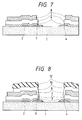
- Fig. 4 is a schematic plan view following the fabricating process of the substrate on the TFT side of the invention and Fig. 7 is a schematic sectional view taken along line C-C' of Fig. 4.
- the substrate was set in an RF plasma CVD apparatus and subjected to PH 3 plasma processing and, thereafter, an a-Si:H film as a semiconductor layer 6 was formed.
- the substrate was kept at a temperature of 250°C and monosilane SiH 4 was used as the material gas.
- the film thickness was set to 18 nm.
- the object in making the film so thin is to suppress the source-drain photoelectric current flowing though the semiconductor layer after the completion of the panel and causing an increase in the off current of the transistor.
- the source-drain photoelectric current is proportional to the cube of the film thickness.
- an SiN layer as a gate insulating film 7 was formed on the substrate in the same chamber.
- the substrate temperature was set to 250°C the same as in the formation of the semiconductor layer, a mixed gas of SiH 4 , NH 3 , and N 2 was used as the material gas, and the film was formed to a thickness of 300 nm.
- a Cr film for the gate wiring 8 was formed to a thickness of 150 nm by a magnetron sputtering method with the substrate kept at a temperature of 100°C.
- the Cr film was subjected to etching and processed into gate electrodes.
- a water solution of Ce(NH 4 ) 2 (NO) 6 with a suitable amount of HNO 3 added thereto was used.
- the gate wiring Cr could be processed to be backward from the patterned width of the semiconductor layer and gate insulating film by about 1.5 ⁇ m on either side. This is indicated by the line on the inside of the gate wiring 8 in Fig. 4. This amount of retreat provides a distance sufficient to prevent occurrence of shorting between the gate electrode 8 and the source electrode 3 as well as the drain wiring 2.
- Fig. 5 is a schematic plan view following the fabricating process of the substrate on the TFT side of the invention.
- Fig. 8 is a schematic sectional view taken along line D-D' of Fig. 5.
- a protective insulating film 10 (SiN) was deposited by an RF plasma CVD method and, thereafter, a resist pattern (holed) 11 for terminal portions of which plane structure is shown in Fig. 5 was formed by photolithographic processing. Then, the protective insulating film was removed by dry etching, and, thereby, the Cr film for the gate wiring terminal portion, the Cr film for the source and drain wiring terminal portion, and the Cr film for the pixel electrode and the source electrode and the additional capacitance electrode connected to the same were exposed. Then, before peeling off the resist 12, an ITO film was deposited thereon to a thickness of 140 nm by sputtering. After the depositing of the ITO film, the resist was peeled off and the ITO film on the resist was lifted off.
- the terminal portions on the substrate on the TFT side are entirely covered with ITO.
- the fabricating condition of the semiconductor layer 6 was changed from that in the embodiment 1.
- a microcrystalline Si film was formed.
- the substrate was kept at a temperature of 300°C and SiF 4 and H 2 was used as the material gas.
- the film thickness was set to 100 nm.
- the characteristic As a result of checking the connection characteristic of the device with peripheral circuits, the characteristic was found to be stable. Also, a good displaying characteristic was obtained.
- Processing down to the step of forming the gate insulating film 7 was performed on a substrate by using the same method as in the embodiment 1. Then, an Al film for the gate wiring 8 was formed by a magnetron sputtering method to a film thickness of 250 nm with the substrate kept at a temperature of 100°C. In succession to the formation of the Al film, a Cr film was formed on the Al film by a magnetron sputtering method to a film thickness of 30 nm. The object of it is to obtain an electric connection between the Cr film and the ITO film at the gate wiring terminal portion. The reason why Al was used is because it has lower resistance than Cr.
- the gate wiring 8, gate insulating film 7, and semiconductor layer 6 were subjected to patterning by photolithography.
- the Cr film was etched by a water solution of cerium (II) nitrate ammonium and, then, the Al film was subjected to over-etching with the use of a water solution of the mixture of phosphoric acid, acetic acid, and nitric acid so that the Al film was retreated from the resist pattern edge portion.
- the Cr film was etched again in the same manner as described above.
- the gate insulating film 7 and the semiconductor layer 6 were subjected to patterning by dry etching.
- the amount of retreat of the gate electrode (Cr/Al) from the pattern width of the semiconductor layer and gate insulating film was about 1.5 ⁇ m on either side.
- a protective insulating film 10 was formed by an RF plasma CVD method and, then, a resist pattern for forming the gate wiring terminal portion, the drain wiring terminal portion and the pixel electrode as shown in Fig. 5 was formed by a photolithographic process.
- the protective insulating film was removed by dry etching, and, thereby, the Cr/Al film for the gate wiring terminal portion, the Cr film for the drain wiring terminal portion, and the Cr film for the source electrode and the additional capacitance electrode connected to the pixel electrode were exposed.
- an ITO film was deposited by sputtering to a thickness of 140 nm. After the ITO film had been deposited, the resist was peeled off and the ITO film on the protective insulating film pattern was lifted off.
- a liquid crystal display device was fabricated using the substrate on the TFT side produced as described above and connected with peripheral circuits. As the result, it was found that a good connection characteristic was obtained. Further, a good displaying characteristic producing little unevenness in brightness was obtained.
- Fig. 11 is a schematic plan view following the fabricating process of the substrate on the TFT side of the invention.
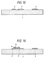
- Fig. 15 is a schematic sectional view taken along line F-F' of Fig. 11.
- the drain wiring 2, source electrode 3, and additional capacitance electrode 4 were formed on a transparent insulating substrate 1.
- Fig. 12 is a schematic plan view following the fabricating process of the substrate on the TFT side of the invention.
- Fig. 16 is a schematic sectional view taken along line G-G' of Fig. 12.
- the substrate was set in an RF plasma CVD apparatus and subjected to a PH 3 plasma treatment and, then, an a-Si:H film for the semiconductor layer 6 was formed by the same method as in the embodiment 1 to a thickness of 18 nm. Then, an SiN film for a first gate insulating layer 16 was formed by the same method as in the embodiment 1 to a thickness of 30 nm. Then, the semiconductor layer 6 and the gate insulating layer 16 were processed using the same mask pattern.
- Fig. 13 is a schematic plan view following the fabricating process of the substrate on the TFT side of the invention.
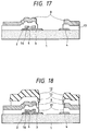
- Fig. 17 is a schematic sectional view taken along line H-H' of Fig. 13.
- the substrate was set in the RF plasma CVD apparatus and an SiN film for a second gate insulating layer 17 was formed by the same method as in the embodiment 1 to a thickness of 270 nm. Then, a Cr film for the gate wiring was formed by the same method as in the embodiment 1.
- Fig. 14 is a schematic plan view following the fabricating process of the substrate on the TFT side of the invention.
- Fig. 18 is a schematic sectional view taken along line I-I' of Fig. 14.
- the second gate insulating layer 17 and the Cr film were subjected to patterning using the same mask pattern and, thereby, the gate wiring 8 was formed.
- the protective insulating film 10 was formed by a plasma CVD method to a thickness of 300 nm. Then, the protective insulating film 10 was removed by a dry etching method and, thereby, the Cr film for the gate wiring terminal portion 9 and the drain wiring terminal portion 5, and the Cr film for the pixel electrode portion and for the source electrode and the additional capacitance electrode connected thereto were exposed. Then, before peeling off of the resist, an ITO film was deposited thereon by sputtering to a thickness of 200 nm. After the ITO film had been deposited, the resist was peeled off and the ITO film on the protective insulating film pattern was lifted off.
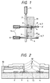
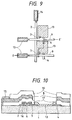
- a TFT substrate as shown in Fig. 9 and Fig. 10 was produced in the described manner.
- a liquid crystal display device was fabricated using the substrate and connected with peripheral circuits. As the result, it was found that a good connection characteristic was obtained. Further, a good displaying characteristic producing little unevenness in brightness was obtained.
- the gate insulating layer is formed of two layers of insulating films, i.e., the first gate insulating layer 16 and the second gate insulating layer 17. Further, as to the auxiliary capacitance, only the second gate insulating layer 17 is inserted between the auxiliary capacitance electrode 4 and the gate wiring 8. At the portion in contact with the semiconductor layer 6 where the channel is formed, there is formed the first gate insulating layer 16 of high insulating quality and, at other portions than that, the second gate insulating layer 17 capable of being formed at a fast film forming speed is formed because the quality of the film is not important there. Thus, the characteristics of the TFT can be improved and, at the same time, the throughput in the fabrication can be increased. Also, the additional capacitance can be formed using the first gate insulating layer 16 of high quality. Further, by decreasing the thickness of the first gate insulating layer, an auxiliary capacitance providing a larger capacitance value with a smaller area can be formed.
- Processing down to the step of forming the gate insulating film 7 was performed by using the same film forming and etching methods as in the embodiment 4. Then, a laminated film of Al 250 nm thick and Cr 30 nm thick for the gate wiring 8 was formed. Thereafter, the gate wiring 8 was subjected to patterning by photolithography in the same method as in the embodiment 3.
- the protective insulating film 10 was formed by a plasma CVD method to a thickness of 300 nm and, then, the protective insulating film was removed by dry etching and the Cr/Al film for the gate wiring terminal portion, the Cr film for the drain wiring terminal portion, and the Cr film for the pixel electrode portion and for the source electrode and the additional capacitance electrode connected to the same were exposed. Then, before peeling off of the resist, an ITO film was deposited thereon by sputtering to a thickness of 200 nm. After the depositing of the ITO film, the resist was peeled off and the ITO film on the protective insulating film pattern was lifted off.
- a liquid crystal display device was fabricated using the substrate on the TFT side produced as described above and connected with peripheral circuits. As the result, it was found that a good connection characteristic was obtained. Further, a good displaying characteristic producing little unevenness in brightness was obtained.
Landscapes
- Physics & Mathematics (AREA)
- Nonlinear Science (AREA)
- Mathematical Physics (AREA)
- Chemical & Material Sciences (AREA)
- Crystallography & Structural Chemistry (AREA)
- General Physics & Mathematics (AREA)
- Optics & Photonics (AREA)
- Engineering & Computer Science (AREA)
- Microelectronics & Electronic Packaging (AREA)
- Liquid Crystal (AREA)
- Thin Film Transistor (AREA)
Applications Claiming Priority (3)
| Application Number | Priority Date | Filing Date | Title |
|---|---|---|---|
| JP12298/95 | 1995-01-30 | ||
| JP1229895A JP3225772B2 (ja) | 1995-01-30 | 1995-01-30 | 液晶表示装置の製造方法 |
| JP1229895 | 1995-01-30 |
Publications (3)
| Publication Number | Publication Date |
|---|---|
| EP0724183A2 true EP0724183A2 (de) | 1996-07-31 |
| EP0724183A3 EP0724183A3 (de) | 1997-03-19 |
| EP0724183B1 EP0724183B1 (de) | 2002-07-31 |
Family
ID=11801428
Family Applications (1)
| Application Number | Title | Priority Date | Filing Date |
|---|---|---|---|
| EP96100908A Expired - Lifetime EP0724183B1 (de) | 1995-01-30 | 1996-01-23 | Flüssigkristall-Anzeige und Verfahren zu ihrer Herstellung |
Country Status (6)
| Country | Link |
|---|---|
| US (1) | US5777702A (de) |
| EP (1) | EP0724183B1 (de) |
| JP (1) | JP3225772B2 (de) |
| KR (1) | KR960029834A (de) |
| CN (1) | CN1075201C (de) |
| DE (1) | DE69622607T2 (de) |
Cited By (3)
| Publication number | Priority date | Publication date | Assignee | Title |
|---|---|---|---|---|
| WO1999004428A1 (de) * | 1997-07-19 | 1999-01-28 | Robert Bosch Gmbh | Verfahren zur herstellung einer matrix aus dünnschichttransistoren mit speicherkapazitäten |
| US7012665B2 (en) | 2002-01-31 | 2006-03-14 | Nec Lcd Technologies, Ltd. | Liquid crystal display device and method for manufacturing the same |
| US7166498B2 (en) | 2002-12-31 | 2007-01-23 | Lg.Philips Lcd Co., Ltd. | Thin film transistor array substrate and manufacturing method of the same |
Families Citing this family (26)
| Publication number | Priority date | Publication date | Assignee | Title |
|---|---|---|---|---|
| US5893624A (en) * | 1996-07-05 | 1999-04-13 | Seiko Instruments Inc. | Liquid crystal display device |
| US6900855B1 (en) | 1995-10-12 | 2005-05-31 | Semiconductor Energy Laboratory Co., Ltd. | Display device having resin black matrix over counter substrate |
| JP3404562B2 (ja) * | 1996-11-18 | 2003-05-12 | 株式会社日立製作所 | アクティブマトリクス型液晶表示装置 |
| KR100244447B1 (ko) * | 1997-04-03 | 2000-02-01 | 구본준 | 액정 표시 장치 및 그 액정 표시 장치의 제조 방법 |
| JPH11101986A (ja) * | 1997-09-26 | 1999-04-13 | Sanyo Electric Co Ltd | 表示装置及び表示装置用大基板 |
| JP3941901B2 (ja) * | 1998-04-28 | 2007-07-11 | 株式会社半導体エネルギー研究所 | 半導体装置の作製方法 |
| KR100291268B1 (ko) * | 1998-07-08 | 2001-07-12 | 윤종용 | 액정표시장치 |
| US6313481B1 (en) | 1998-08-06 | 2001-11-06 | Semiconductor Energy Laboratory Co., Ltd. | Semiconductor device and a method of manufacturing the same |
| JP2000275663A (ja) * | 1999-03-26 | 2000-10-06 | Hitachi Ltd | 液晶表示装置とその製造方法 |
| JP3916349B2 (ja) * | 1999-06-15 | 2007-05-16 | 株式会社アドバンスト・ディスプレイ | 液晶表示装置 |
| KR100498630B1 (ko) * | 1999-09-01 | 2005-07-01 | 엘지.필립스 엘시디 주식회사 | 액정표시장치 |
| KR100668251B1 (ko) * | 2000-02-21 | 2007-01-12 | 엘지.필립스 엘시디 주식회사 | 기판의 내장홈 형성방법 |
| JP3516441B2 (ja) * | 2000-07-10 | 2004-04-05 | インターナショナル・ビジネス・マシーンズ・コーポレーション | アクティブマトリックス基板、表示装置、およびアクティブマトリックス基板の製造方法 |
| KR100469345B1 (ko) * | 2001-11-22 | 2005-02-02 | 엘지.필립스 엘시디 주식회사 | 액정 디스플레이 패널 제조방법 |
| KR100483988B1 (ko) | 2001-11-29 | 2005-04-15 | 삼성에스디아이 주식회사 | 투명도전막의 투과도 변형방법 |
| TWI241430B (en) * | 2002-03-01 | 2005-10-11 | Prime View Int Corp Ltd | Method for forming a bonding pad in a TFT array process for a reflective LCD and bonding pad formed by the same |
| TWI272556B (en) * | 2002-05-13 | 2007-02-01 | Semiconductor Energy Lab | Display device |
| KR100606446B1 (ko) | 2002-12-27 | 2006-07-31 | 엘지.필립스 엘시디 주식회사 | 액정표시소자의 제조방법 |
| KR100560399B1 (ko) | 2003-11-04 | 2006-03-14 | 엘지.필립스 엘시디 주식회사 | 수평 전계 인가형 박막 트랜지스터 기판 및 그 제조 방법 |
| KR101282397B1 (ko) * | 2004-12-07 | 2013-07-04 | 삼성디스플레이 주식회사 | 표시 장치용 배선, 상기 배선을 포함하는 박막 트랜지스터표시판 및 그 제조 방법 |
| TW200710471A (en) * | 2005-07-20 | 2007-03-16 | Samsung Electronics Co Ltd | Array substrate for display device |
| CN100498491C (zh) * | 2005-10-26 | 2009-06-10 | 中华映管股份有限公司 | 液晶显示器及其薄膜晶体管阵列基板 |
| JP5261384B2 (ja) * | 2006-07-17 | 2013-08-14 | 三星電子株式会社 | 透明導電ナノ構造膜画素電極およびその製造方法 |
| US8785939B2 (en) * | 2006-07-17 | 2014-07-22 | Samsung Electronics Co., Ltd. | Transparent and conductive nanostructure-film pixel electrode and method of making the same |
| JP5810810B2 (ja) * | 2011-10-04 | 2015-11-11 | 大日本印刷株式会社 | トップゲート型アクティブマトリックス基板、およびその製造方法 |
| CN111799280A (zh) | 2020-07-20 | 2020-10-20 | 京东方科技集团股份有限公司 | 显示基板及其制备方法、显示装置 |
Family Cites Families (8)
| Publication number | Priority date | Publication date | Assignee | Title |
|---|---|---|---|---|
| JP2786628B2 (ja) * | 1987-10-15 | 1998-08-13 | シャープ株式会社 | 液晶パネルの電極構造 |
| US5187604A (en) * | 1989-01-18 | 1993-02-16 | Hitachi, Ltd. | Multi-layer external terminals of liquid crystal displays with thin-film transistors |
| KR960014823B1 (ko) * | 1991-03-15 | 1996-10-21 | 가부시기가이샤 히다찌세이사구쇼 | 액정표시장치 |
| JPH05142554A (ja) * | 1991-11-25 | 1993-06-11 | Matsushita Electric Ind Co Ltd | アクテイブマトリクス基板 |
| JP3392440B2 (ja) * | 1991-12-09 | 2003-03-31 | 株式会社東芝 | 多層導体層構造デバイス |
| JPH05323375A (ja) * | 1992-05-25 | 1993-12-07 | Sanyo Electric Co Ltd | 液晶表示装置 |
| JPH06250211A (ja) * | 1993-02-23 | 1994-09-09 | Hitachi Ltd | 液晶表示基板とその製造方法 |
| US5691782A (en) * | 1994-07-08 | 1997-11-25 | Sanyo Electric Co., Ltd. | Liquid-crystal display with inter-line short-circuit preventive function and process for producing same |
-
1995
- 1995-01-30 JP JP1229895A patent/JP3225772B2/ja not_active Expired - Fee Related
-
1996
- 1996-01-18 US US08/588,446 patent/US5777702A/en not_active Expired - Fee Related
- 1996-01-23 EP EP96100908A patent/EP0724183B1/de not_active Expired - Lifetime
- 1996-01-23 DE DE69622607T patent/DE69622607T2/de not_active Expired - Fee Related
- 1996-01-29 KR KR1019960001879A patent/KR960029834A/ko not_active Abandoned
- 1996-01-30 CN CN96102587A patent/CN1075201C/zh not_active Expired - Fee Related
Cited By (6)
| Publication number | Priority date | Publication date | Assignee | Title |
|---|---|---|---|---|
| WO1999004428A1 (de) * | 1997-07-19 | 1999-01-28 | Robert Bosch Gmbh | Verfahren zur herstellung einer matrix aus dünnschichttransistoren mit speicherkapazitäten |
| US7012665B2 (en) | 2002-01-31 | 2006-03-14 | Nec Lcd Technologies, Ltd. | Liquid crystal display device and method for manufacturing the same |
| US7518667B2 (en) | 2002-01-31 | 2009-04-14 | Nec Lcd Technologies, Ltd. | Method for manufacturing a liquid crystal display device |
| US7166498B2 (en) | 2002-12-31 | 2007-01-23 | Lg.Philips Lcd Co., Ltd. | Thin film transistor array substrate and manufacturing method of the same |
| DE10355666B4 (de) * | 2002-12-31 | 2007-07-19 | Lg. Philips Lcd Co., Ltd. | Dünnschichttransistor-Matrixsubstrat sowie Verfahren zu dessen Herstellung |
| US7411217B2 (en) | 2002-12-31 | 2008-08-12 | Lg Display Co., Ltd. | Thin film transistor array substrate and manufacturing method of the same |
Also Published As
| Publication number | Publication date |
|---|---|
| EP0724183B1 (de) | 2002-07-31 |
| EP0724183A3 (de) | 1997-03-19 |
| DE69622607D1 (de) | 2002-09-05 |
| JP3225772B2 (ja) | 2001-11-05 |
| KR960029834A (ko) | 1996-08-17 |
| DE69622607T2 (de) | 2003-03-13 |
| CN1153313A (zh) | 1997-07-02 |
| CN1075201C (zh) | 2001-11-21 |
| US5777702A (en) | 1998-07-07 |
| JPH08201849A (ja) | 1996-08-09 |
Similar Documents
| Publication | Publication Date | Title |
|---|---|---|
| US5777702A (en) | Liquid crystal display device and method of fabricating the same by patterning semiconductor, insulator, and gatelines with single mask | |
| US4958205A (en) | Thin film transistor array and method of manufacturing the same | |
| JP3238020B2 (ja) | アクティブマトリクス表示装置の製造方法 | |
| US6323051B1 (en) | Method of manufacturing liquid crystal display | |
| US6624864B1 (en) | Liquid crystal display device, matrix array substrate, and method for manufacturing matrix array substrate | |
| US5917564A (en) | Methods of forming active matrix display devices with reduced susceptibility to image-sticking and devices formed thereby | |
| US6608658B1 (en) | Top gate TFT structure having light shielding layer and method to fabricate the same | |
| US9716110B2 (en) | Array substrate, method for manufacturing the same, and display device | |
| KR19990017836A (ko) | 박막트랜지스터 및 그의 제조방법 | |
| JP4169811B2 (ja) | 薄膜トランジスタの製造方法 | |
| US6395457B1 (en) | Method for manufacturing a semiconductor device | |
| JPH08146446A (ja) | アクティブマトリクス型液晶表示装置 | |
| JPH06208137A (ja) | 薄膜トランジスタマトリクスの製造方法 | |
| US6376288B1 (en) | Method of forming thin film transistors for use in a liquid crystal display | |
| JP2000002886A (ja) | 液晶表示装置の製造方法 | |
| US6335781B2 (en) | Method for manufacturing an LCD in which a photoresist layer is at least 1.2 times thicker than the passivation layer | |
| JP3234168B2 (ja) | Tftアレイ基板の製造方法 | |
| KR100272255B1 (ko) | 박막트랜지스터제조방법 | |
| US7116389B2 (en) | Liquid crystal display device and method of manufacturing the same | |
| JPH0926598A (ja) | アクティブマトリクス型液晶ディスプレイ装置 | |
| KR100663288B1 (ko) | 박막 트랜지스터 액정표시장치의 제조방법 | |
| JP2966142B2 (ja) | アモルファスシリコン薄膜トランジスタアレイ | |
| KR100205867B1 (ko) | 액티브매트릭스기판의 제조방법 및 그 방법에 의해제조되는액티브매트릭스기판 | |
| JPH0822029A (ja) | 液晶表示装置及びその製造方法 | |
| JP3079600B2 (ja) | マトリックス型表示装置の製造方法 |
Legal Events
| Date | Code | Title | Description |
|---|---|---|---|
| PUAI | Public reference made under article 153(3) epc to a published international application that has entered the european phase |
Free format text: ORIGINAL CODE: 0009012 |
|
| AK | Designated contracting states |
Kind code of ref document: A2 Designated state(s): CH DE FR GB LI NL |
|
| PUAL | Search report despatched |
Free format text: ORIGINAL CODE: 0009013 |
|
| AK | Designated contracting states |
Kind code of ref document: A3 Designated state(s): CH DE FR GB LI NL |
|
| 17P | Request for examination filed |
Effective date: 19970210 |
|
| 17Q | First examination report despatched |
Effective date: 19970723 |
|
| GRAG | Despatch of communication of intention to grant |
Free format text: ORIGINAL CODE: EPIDOS AGRA |
|
| GRAG | Despatch of communication of intention to grant |
Free format text: ORIGINAL CODE: EPIDOS AGRA |
|
| GRAH | Despatch of communication of intention to grant a patent |
Free format text: ORIGINAL CODE: EPIDOS IGRA |
|
| GRAH | Despatch of communication of intention to grant a patent |
Free format text: ORIGINAL CODE: EPIDOS IGRA |
|
| GRAA | (expected) grant |
Free format text: ORIGINAL CODE: 0009210 |
|
| AK | Designated contracting states |
Kind code of ref document: B1 Designated state(s): CH DE FR GB LI NL |
|
| REG | Reference to a national code |
Ref country code: GB Ref legal event code: FG4D Ref country code: CH Ref legal event code: EP |
|
| REG | Reference to a national code |
Ref country code: CH Ref legal event code: NV Representative=s name: TROESCH SCHEIDEGGER WERNER AG |
|
| REF | Corresponds to: |
Ref document number: 69622607 Country of ref document: DE Date of ref document: 20020905 |
|
| ET | Fr: translation filed | ||
| PGFP | Annual fee paid to national office [announced via postgrant information from national office to epo] |
Ref country code: GB Payment date: 20030113 Year of fee payment: 8 |
|
| PGFP | Annual fee paid to national office [announced via postgrant information from national office to epo] |
Ref country code: FR Payment date: 20030117 Year of fee payment: 8 |
|
| PGFP | Annual fee paid to national office [announced via postgrant information from national office to epo] |
Ref country code: NL Payment date: 20030131 Year of fee payment: 8 |
|
| PGFP | Annual fee paid to national office [announced via postgrant information from national office to epo] |
Ref country code: CH Payment date: 20030328 Year of fee payment: 8 |
|
| PGFP | Annual fee paid to national office [announced via postgrant information from national office to epo] |
Ref country code: DE Payment date: 20030331 Year of fee payment: 8 |
|
| PLBE | No opposition filed within time limit |
Free format text: ORIGINAL CODE: 0009261 |
|
| STAA | Information on the status of an ep patent application or granted ep patent |
Free format text: STATUS: NO OPPOSITION FILED WITHIN TIME LIMIT |
|
| 26N | No opposition filed |
Effective date: 20030506 |
|
| PG25 | Lapsed in a contracting state [announced via postgrant information from national office to epo] |
Ref country code: GB Free format text: LAPSE BECAUSE OF NON-PAYMENT OF DUE FEES Effective date: 20040123 |
|
| PG25 | Lapsed in a contracting state [announced via postgrant information from national office to epo] |
Ref country code: LI Free format text: LAPSE BECAUSE OF NON-PAYMENT OF DUE FEES Effective date: 20040131 Ref country code: CH Free format text: LAPSE BECAUSE OF NON-PAYMENT OF DUE FEES Effective date: 20040131 |
|
| PG25 | Lapsed in a contracting state [announced via postgrant information from national office to epo] |
Ref country code: NL Free format text: LAPSE BECAUSE OF NON-PAYMENT OF DUE FEES Effective date: 20040801 |
|
| PG25 | Lapsed in a contracting state [announced via postgrant information from national office to epo] |
Ref country code: DE Free format text: LAPSE BECAUSE OF NON-PAYMENT OF DUE FEES Effective date: 20040803 |
|
| GBPC | Gb: european patent ceased through non-payment of renewal fee |
Effective date: 20040123 |
|
| REG | Reference to a national code |
Ref country code: CH Ref legal event code: PL |
|
| PG25 | Lapsed in a contracting state [announced via postgrant information from national office to epo] |
Ref country code: FR Free format text: LAPSE BECAUSE OF NON-PAYMENT OF DUE FEES Effective date: 20040930 |
|
| NLV4 | Nl: lapsed or anulled due to non-payment of the annual fee |
Effective date: 20040801 |
|
| REG | Reference to a national code |
Ref country code: FR Ref legal event code: ST |