EP0725923B1 - Zweipoliger temperatursensor mit schaltung zur überwachung der linearen proportionalität des ganzen betriebsstroms - Google Patents
Zweipoliger temperatursensor mit schaltung zur überwachung der linearen proportionalität des ganzen betriebsstroms Download PDFInfo
- Publication number
- EP0725923B1 EP0725923B1 EP94931437A EP94931437A EP0725923B1 EP 0725923 B1 EP0725923 B1 EP 0725923B1 EP 94931437 A EP94931437 A EP 94931437A EP 94931437 A EP94931437 A EP 94931437A EP 0725923 B1 EP0725923 B1 EP 0725923B1
- Authority
- EP
- European Patent Office
- Prior art keywords
- temperature
- voltage
- transducer
- transistor
- reference voltage
- Prior art date
- Legal status (The legal status is an assumption and is not a legal conclusion. Google has not performed a legal analysis and makes no representation as to the accuracy of the status listed.)
- Expired - Lifetime
Links
Images



Classifications
-
- G—PHYSICS
- G05—CONTROLLING; REGULATING
- G05F—SYSTEMS FOR REGULATING ELECTRIC OR MAGNETIC VARIABLES
- G05F3/00—Non-retroactive systems for regulating electric variables by using an uncontrolled element, or an uncontrolled combination of elements, such element or such combination having self-regulating properties
- G05F3/02—Regulating voltage or current
- G05F3/08—Regulating voltage or current wherein the variable is DC
- G05F3/10—Regulating voltage or current wherein the variable is DC using uncontrolled devices with non-linear characteristics
- G05F3/16—Regulating voltage or current wherein the variable is DC using uncontrolled devices with non-linear characteristics being semiconductor devices
- G05F3/20—Regulating voltage or current wherein the variable is DC using uncontrolled devices with non-linear characteristics being semiconductor devices using diode- transistor combinations
- G05F3/30—Regulators using the difference between the base-emitter voltages of two bipolar transistors operating at different current densities
-
- G—PHYSICS
- G01—MEASURING; TESTING
- G01K—MEASURING TEMPERATURE; MEASURING QUANTITY OF HEAT; THERMALLY-SENSITIVE ELEMENTS NOT OTHERWISE PROVIDED FOR
- G01K7/00—Measuring temperature based on the use of electric or magnetic elements directly sensitive to heat ; Power supply therefor, e.g. using thermoelectric elements
- G01K7/01—Measuring temperature based on the use of electric or magnetic elements directly sensitive to heat ; Power supply therefor, e.g. using thermoelectric elements using semiconducting elements having PN junctions
-
- Y—GENERAL TAGGING OF NEW TECHNOLOGICAL DEVELOPMENTS; GENERAL TAGGING OF CROSS-SECTIONAL TECHNOLOGIES SPANNING OVER SEVERAL SECTIONS OF THE IPC; TECHNICAL SUBJECTS COVERED BY FORMER USPC CROSS-REFERENCE ART COLLECTIONS [XRACs] AND DIGESTS
- Y10—TECHNICAL SUBJECTS COVERED BY FORMER USPC
- Y10S—TECHNICAL SUBJECTS COVERED BY FORMER USPC CROSS-REFERENCE ART COLLECTIONS [XRACs] AND DIGESTS
- Y10S323/00—Electricity: power supply or regulation systems
- Y10S323/907—Temperature compensation of semiconductor
Definitions
- the invention relates to temperature sensing devices, and more particularly to such devices using the temperature sensitive properties of transistors.
- thermocouples such as thermocouples, thermistors, or RTDs
- RTDs thermocouples, thermistors, or RTDs
- Thermocouples require accurate cold junction compensation, some form of linearization, and produce a low level voltage output which is subject to electrical noise interference.
- Resistance thermometers and thermistors have a non-linear characteristic which requires careful compensation and a wide dynamic electrical range.
- making a good resistance measurement demands an accurate voltage source, low level precision current sensing, and careful lead compensation.
- These devices also require strict attention to lead wire material connections. Initial calibration on all of these devices is also a problem, especially when field replacement is necessary.
- a two terminal temperature transducer 10 illustrated in Fig. 1 generates an output current I T varying with absolute temperature by means of first and second transistors Q1 and Q2 operated at a constant ratio of emitter current densities, and having their bases interconnected and the difference between their respective V be impressed across a resistor R.
- J e J s (e q V be KT -1)
- J s the emitter saturation current density
- q the charge in coulombs of an electron
- K the Boltzman's constant
- T absolute temperature.
- the (-1) term is very small and is usually neglected.
- the ratio of emitter current densities also will be r, and the difference voltage ⁇ V be is directly proportional to absolute temperature.
- the voltage ⁇ V be appears across resistor R and determines the level of current flowing through transistor Q1.
- the output current I T drawn by both sides of the circuit is
- I T is also directly proportional to absolute temperature, and appropriate selection of the emitter ratio r and resistance R will provide an output current accurately related to temperature with a predetermined constant of proportionality, useful for absolute temperature sensing purposes.
- the device is generally specified only for operation to -55°C or 218°K and is useful at somewhat lower temperatures.
- the transducer 10 In order to measure a small temperature range using the transducer 10, it is necessary to suppress at least the first 218°K worth of its output signal, or more typically, the first 273°K in order to refer a conditioned output signal to 0°C.
- This suppression is an inconvenience and a possible source of error with a degradation of signal-to-noise ratio.
- the zero suppression involves an additional reference signal which must be temperature insensitive, and any error in this reference reflects as an error in the conditioned output.
- the principle of operation of the present invention is to pass the operating current of a circuit through a single resistor, to compare the resulting voltage drop to a temperature sensitive voltage, and to adjust the total operating current so that the resistor voltage matches the temperature sensitive voltage.
- the temperature sensitive voltage is made to be proportional to temperature and to pass through zero at the extrapolated zero point desired for the transducer.
- the present invention provides a two terminal temperature transducer including circuitry which controls its operating current to be linearly proportional with temperature.
- the circuitry of the transducer includes means for producing a first reference voltage which is proportional to absolute temperature; means for producing a second reference voltage which is complementary to absolute temperatures; means for generating a voltage drop corresponding to the operating current; means for comparing the voltage drop to a temperature sensitive voltage corresponding to the difference between the first reference voltage and the second reference voltage; and means for adjusting the operating current so as to equilibrate the voltage drop and the temperature sensitive voltage.
- a two terminal temperature transducer including circuitry which produces an output current that varies linearly with temperature.
- the circuitry includes a differential input stage including first and second transistors having differing operational current densities, and current supplying means for supplying current through the first and second transistors to operate the first and second transistors at different current densities and to produce a difference between the respective base-to-emitter voltages, the difference in base-to-emitter voltages corresponding to a first reference voltage which is proportional to absolute temperature.
- a third transistor having a base-to-emitter voltage corresponding to a second reference voltage which is complementary to absolute temperature, the third transistor being coupled to the differential input stage so that a portion of the base-to-emitter voltage of the third transistor equals the difference in base-to-emitter voltages of the first and second transistors at a predetermined temperature.
- Converting means are provided for converting the difference between the first reference voltage and the second reference voltage into the output current.
- a two terminal temperature transducer 20 in accordance with the present invention operates in accordance with the temperature effects on the base-to-emitter voltage of a transistor and the difference between that voltage and the base-to-emitter voltage of a matched transistor. For example, when two matched transistors are operated at different current densities, their base-to-emitter voltages differ by an amount proportional to absolute temperature (PTAT). This voltage is given by equation (4) provided above.
- the base-to-emitter voltage of a transistor is dependably temperature sensitive as it falls to zero at a temperature related to how the transistor is made and the collector current of the device. If this decline is extrapolated to low temperatures, however, the voltage at zero (absolute) will be nearly independent of how the transistor is made, as long as the collector current function used has zero as its limit at zero and is positive for all other positive transistor temperatures. In other words, the temperature behavior of the base-to-emitter voltage around room temperature can be extrapolated toward a single value at zero. If the collector current is made to be PTAT, the voltage intercept at zero will be almost independent of how the transistor is made or of the actual room temperature bias current. The intercept approximates the extrapolated band gap voltage. This extrapolated voltage is the complement of a PTAT voltage with respect to the intercept value of the band gap voltage or is complementary to absolute temperature (CTAT).
- CTAT absolute temperature
- a plot of a voltage scaled from the idealized base-to-emitter voltage and a CTAT voltage tangent to it is shown.
- the plot also includes a PTAT voltage proportional to the ⁇ V be of transistors operated at different current densities. These voltages are assumed to have been adjusted relative to one another, so that they are at a selected temperature, thus making their difference zero.
- the PTAT and CTAT voltages so adjusted now produce a difference voltage above the selected temperature.
- the circuit may have an extrapolated zero point of -70°C and be intended to operate in the range above -55°C with a scale of 5 ⁇ A/°C. Accordingly, a minimum of 75 ⁇ A ((70° - 55°) x 5 ⁇ A/°C) is available to operate the circuit.
- the circuit When the temperature is above the value corresponding to the keep-alive current, the circuit operates as a current sink loading its supply terminals to the proper load current.
- Fig. 4 shows an I-T curve illustrating how the actual device sink current might depart from ideal at low temperatures.
- the transducer 20 includes a differential input stage 22 having transistors Q1, Q2, Q3, and Q4 arranged so that the inputs can go slightly negative with respect to the remainder of the transducer circuitry, and the differential output current is drawn from the positive direction by transistors Q3 and Q4.
- the differential input stage includes a bias current supply 24 coupled between the bases of Q3 and Q4 and the collectors of Q1 and Q2.
- the output currents of Q3 and Q4 develop a voltage across the two load resistors R4 and R5 coupled thereto. Any difference in the currents will result in a difference voltage at the ends of the load resistors which drives the inputs of an op-amp 26. Any difference voltage derived by the load resistors will cause the amplifier to drive a transistor Q5 to increase or decrease the current supply to a reference node VL. Coupled to the node VL is a resistor R6 which functions as the sensing resistor placed in series with the entire circuitry of the transducer 20, except for the base current of transistor Q1, which may be made small and relatively repeatable. Thus, as the amplifier 26 drives transistor Q5, the current through the resistor R6 is increased or decreased accordingly.
- connections of the circuitry are phased so that the resulting change in voltage across resistor R6 tends to reduce the difference in the collector currents of transistors Q3 and Q4. Accordingly, the operating point of the transducer 20 will move toward an equilibrium which equalizes the collector currents of transistors Q3 and Q4.
- transistor Q4 is configured with multiple emitters so that it will be operating at reduced current density when its collector current matches that of transistor Q3.
- the base-to-emitter voltages of the transistors Q3 and Q4 will differ by the amount ⁇ V be as described in equation (4).
- the differences between the base-to-emitter voltages becomes which is equivalent to approximately 36mV at room temperature.
- the reduced current density of transistor Q4 may also be achieved by configuring either both transistor Q4 and transistor Q2 or only Q2 with multiple emitters.
- This voltage will be proportional to T, the Kelvin temperature, so long as the collector currents are held in balance. If the circuit loop of the transducer 20 operated to force this voltage across the resistor R6, the output current would be PTAT, similar to that of the transducer 10 shown in Fig. 1. However, the base of transistor Q2 is coupled to a fraction of the base-to-emitter voltage of a transistor Q6. The transistor Q6 along with a bias current source 28 is configured in parallel to the input differential stage 22. The transistor Q6 includes a voltage divider made up of resistors R1 and R2 disposed across the base and emitter of the transistor Q6. The portion of the base-to-emitter voltage of the transistor Q6 appearing across resistor R2 will be CTAT, as it falls with increasing temperature.
- this voltage may be selected to equal ⁇ V be of the transistors Q3 and Q4 at a predetermined temperature.
- the circuit loop would be in balance with zero volts across the resistor R6, since the base of the transistor Q2 will be ⁇ V be above the voltage at the node VL.
- the voltage applied to the base of the transistor Q2 will fall, while the ⁇ V be required fcr balance will rise.
- the circuit loop will force a temperature proportional current to flow in the resistor R6. Accordingly, the transducer 20 will operate to closely approximate the temperature proportional characteristic desired, at temperatures which correspond to currents larger than the operating minimum.
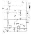
- Fig. 5 a more detailed schematic of the two terminal temperature transducer 20 of Fig. 2 is shown.
- Figs. 6A and 6B show plots of a simulated temperature sweep of the circuit in Fig. 5, from -55°C to 155°C, showing the current drawn as a function of temperature, and the non-linearity of the response.
- the circuit has been configured to have a slope of about 5 ⁇ A/°C and an intercept of -70°C.
- the transducers utilize NPN transistors to form the ⁇ V be , since the NPN transistors found in common processes are superior for these purposes.
- the sensing resistor R6 may be placed in the positive lead of the transducer and measured relatively easily. By inverting the input circuitry utilizing NPN transistors as the input and PNP transistors as level shifters, the transducer could compare the resistor R6 voltage to a fraction of a V be connected to the positive lead.
- a further modification to the transducer of Fig. 2 is the implementation of curvature correction.
- the V be of transistor Q6 falls approximately in proportion to temperature, however, there is a small component of higher order temperature sensitivity causing the voltage to curve slightly.
- This curvature can be corrected in the transducer of the present invention, as is done in band-gap references.
- a small resistance having a positive temperature coefficient can be added in series with the resistor R6 to produce a slight curvature in the overall VI characteristic over temperature. This can be adjusted to reduce the curvature resulting from the V be of transistor Q6.
- temperature sensitive resistors can be used in the transistor Q6 voltage divider to compensate for the curvature.
- Additional features which may be included in the transducer of the present invention include additional resistances similar to resistor R6 which are provided as connection options to program the sensitivity.
- the voltage divider associated with transistor Q6 may also have pin selectable taps, to permit user selection of the zero point.
Landscapes
- Engineering & Computer Science (AREA)
- Physics & Mathematics (AREA)
- General Physics & Mathematics (AREA)
- Microelectronics & Electronic Packaging (AREA)
- Power Engineering (AREA)
- Nonlinear Science (AREA)
- Electromagnetism (AREA)
- Radar, Positioning & Navigation (AREA)
- Automation & Control Theory (AREA)
- Indication And Recording Devices For Special Purposes And Tariff Metering Devices (AREA)
- Measuring Temperature Or Quantity Of Heat (AREA)
- Amplifiers (AREA)
Claims (21)
- Zwei-Anschluß-Temperaturwandler mit einer Schaltungsanordnung, welche seinen gesamten Betriebsstrom derart steuert, daß er linear proportional zur Temperatur ist, wobei die Schaltungsanordnung aufweist:eine Einrichtung zum Erzeugen einer ersten Referenzspannung, welche proportional zur absoluten Temperatur ist;eine Einrichtung zum Erzeugen einer zweiten Referenzspannung, welche komplementär zur absoluten Temperatur ist;eine Einrichtung zum Erzeugen eines Spannungsabfalls entsprechend dem gesamten Betriebsstrom, welcher durch die zwei Anschlüsse fließt;eine Einrichtung zum Vergleichen des Spannungsabfalls mit einer temperaturempfindlichen Spannung entsprechend der Differenz zwischen der ersten Referenzspannung und der zweiten Referenzspannung; undeine Einrichtung zum derartigen Einstellen des gesamten Betriebsstroms, daß der Spannungsabfall und die temperaturempfindliche Spannung im Gleichgewicht stehen.
- Wandler nach Anspruch 1,
dadurch gekennzeichnet,
daß die Einrichtung zum Erzeugen der ersten Referenzspannung einen ersten und einen zweiten Transistor aufweist, welcher eine Differenz zwischen der jeweiligen Basis-Emitter-Spannung entsprechend der ersten Referenzspannung erzeugen. - Wandler nach Anspruch 2,
dadurch gekennzeichnet,
daß der erste Transistor mit einer anderen Stromdichte als der zweite Transistor zur Anpassung der Kollektorströme arbeitet. - Wandler nach Anspruch 2,
dadurch gekennzeichnet,
daß der erste Transistor elektrisch mit der Einrichtung zum Erzeugen der zweiten Referenzspannung verbunden ist. - Wandler nach Anspruch 4,
dadurch gekennzeichnet,
daß die Einrichtung zum Erzeugen der zweiten Referenzspannung einen dritten Transistor mit einer zugehörigen Basis-Emitter-Spannung aufweist, wobei die zweite Referenzspannung einem vorbestimmten Anteil der Basis-Emitter-Spannung des dritten Transistors entspricht. - Wandler nach Anspruch 5,
dadurch gekennzeichnet,
daß eine Nullausgabe für den Wandler ansprechend darauf erfolgt, daß die Differenz zwischen der jeweiligen Basis-Emitter-Spannung des ersten und zweiten Transistors gleich dem vorbestimmten Anteil der Basis-Emitter-Spannung des dritten Transistors ist. - Wandler nach Anspruch 1,
dadurch gekennzeichnet,
daß die Einrichtung zum Erzeugen eines Spannungsabfalls einen Spannungsabfall von Null darauf ansprechend erzeugt, daß die erste und zweite Referenzspannung gleich sind. - Wandler nach Anspruch 7,
dadurch gekennzeichnet,
daß der Spannungsabfall von Null einer Referenz-Nulltemperatur entspricht. - Wandler nach Anspruch 1,
dadurch gekennzeichnet,
daß die Einrichtung zum Erzeugen eines Spannungsabfalls einen Widerstand aufweist, der in Reihe sowohl mit der Einrichtung zum Erzeugen der ersten Referenzspannung als auch mit der Einrichtung zum Erzeugen der zweiten Referenzspannung angeschlossen ist. - Zwei-Anschluß-Temperaturwandler mit einer Schaltungsanordnung, welche ein Ausgangssignal erzeugt, welche der gesamte Betriebsstrom ist, der linear mit der Temperatur variiert, wobei die Schaltungsanordnung aufweist:eine differentielle Eingangsstufe mit einem ersten und einem zweiten Transistor mit verschiedenen Betriebsstromdichten;eine Stromversorgungseinrichtung zum Zuführen eines Stroms durch den ersten und zweiten Transistor zum Betreiben des ersten und zweiten Transistors bei verschiedenen Stromdichten und zum Erzeugen einer Differenz zwischen der jeweiligen Basis-Emitter-Spannung, wobei die Differenz der Basis-Emitter-Spannungen einer ersten Referenzspannung entspricht, welche proportional zur absoluten Temperatur ist;einen dritten Transistor mit einer Basis-Emitter-Spannung entsprechend einer zweiten Referenzspannung, die komplementär zur absoluten Temperatur ist, wobei der dritte Transistor derart mit der differentiellen Eingangsstufe verbunden ist, daß ein Anteil der Basis-Emitter-Spannung des dritten Transistors der Differenz der Basis-Emitter-Spannungen des ersten und zweiten Transistors bei einer vorbestimmten Temperatur gleicht; undeine Umwandlungseinrichtung zum Umwandeln der Differenz zwischen der ersten Referenzspannung und der zweiten Referenzspannung in den gesamten Betriebsstrom, welcher an den zwei Anschlüssen als das Ausgangssignal bereitstellbar ist.
- Wandler nach Anspruch 10,
dadurch gekennzeichnet,
daß eine extrapolierte Nullausgabe für den Wandler darauf ansprechend erzeugbar ist, daß die Differenz der Basis-Emitter-Spannungen des ersten und zweiten Transistors gleich dem vorbestimmten Anteil der Basis-Emitter-Spannung des dritten Transistors bei der vorbestimmten Temperatur ist. - Wandler nach Anspruch 11,
dadurch gekennzeichnet,
daß die extrapolierte Nullausgabe einer Nullreferenztemperatur entspricht. - Wandler nach Anspruch 10,
dadurch gekennzeichnet,
daß ein Temperatur-proportionaler Strom an die Umwandlungseinrichtung ansprechend auf eine Temperaturvariation lieferbar ist. - Wandler nach Anspruch 10,
gekennzeichnet durch eine Korrektureinrichtung zum Korrigieren der temperaturempfindlichen Variationen der Basis-Emitter-Spannung des dritten Transistors. - Wandler nach Anspruch 14,
dadurch gekennzeichnet,
daß die Korrektureinrichtung einen Widerstand mit einem positiven Temperaturkoeffizienten aufweist, welcher in Reihe mit der Umwandlungseinrichtung geschaltet ist. - Wandler nach Anspruch 10,
dadurch gekennzeichnet,
daß der erste Transistor mit einem Spannungsteiler verbunden ist, der der Basis und dem Emitter des dritten Transistors zugeordnet ist. - Wandler nach Anspruch 16,
dadurch gekennzeichnet,
daß der Spannungsteiler Anschlußstift-auswählbare Abgriffe aufweist. - Wandler nach Anspruch 11,
dadurch gekennzeichnet,
daß der Transistor eine Vielzahl von Emittern aufweist, um bei einer anderen Stromdichte als der zweite Transistor zu arbeiten. - Wandler nach Anspruch 11,
dadurch gekennzeichnet,
daß der dritte Transistor mit dem ersten Transistor über einen vierten Transistor verbunden ist. - Wandler nach Anspruch 19,
dadurch gekennzeichnet,
daß der vierte Transistor eine Vielzahl von Emittern aufweist, um den ersten Transistor bei einer anderen Stromdichte als den zweiten Transistor zu betreiben. - Verfahren zum Steuern des gesamten Betriebsstroms eines Zwei-Anschluß-Temperaturwandlers, so daß er proportional zur Temperatur ist, wobei das Verfahren folgende Schritte aufweist:Erzeugen einer ersten Referenzspannung, welche proportional zur absoluten Temperatur ist;Erzeugen einer zweiten Referenzspannung, welche komplementär zur absoluten Temperatur ist,Erzeugen eines Spannungsabfalls entsprechend dem gesamten Betriebsstrom, der durch die zwei Anschlüsse fließt;Vergleichen des Spannungsabfalls mit einer temperaturempfindlichen Spannung entsprechend der Differenz zwischen der ersten Referenzspannung und der zweiten Referenzspannung; undEinstellen des gesamten Betriebsstroms, um den Spannungsabfall und die temperaturempfindliche Spannung ins Gleichgewicht zu bringen.
Applications Claiming Priority (3)
| Application Number | Priority Date | Filing Date | Title |
|---|---|---|---|
| US142768 | 1993-10-26 | ||
| US08/142,768 US5394078A (en) | 1993-10-26 | 1993-10-26 | Two terminal temperature transducer having circuitry which controls the entire operating current to be linearly proportional with temperature |
| PCT/US1994/012142 WO1995012115A1 (en) | 1993-10-26 | 1994-10-25 | Two terminal temperature transducer having circuitry which controls the entire operating current to be linearly proportional with temperature |
Publications (2)
| Publication Number | Publication Date |
|---|---|
| EP0725923A1 EP0725923A1 (de) | 1996-08-14 |
| EP0725923B1 true EP0725923B1 (de) | 1998-08-05 |
Family
ID=22501193
Family Applications (1)
| Application Number | Title | Priority Date | Filing Date |
|---|---|---|---|
| EP94931437A Expired - Lifetime EP0725923B1 (de) | 1993-10-26 | 1994-10-25 | Zweipoliger temperatursensor mit schaltung zur überwachung der linearen proportionalität des ganzen betriebsstroms |
Country Status (6)
| Country | Link |
|---|---|
| US (1) | US5394078A (de) |
| EP (1) | EP0725923B1 (de) |
| JP (1) | JPH09504373A (de) |
| AT (1) | ATE169401T1 (de) |
| DE (1) | DE69412277T2 (de) |
| WO (1) | WO1995012115A1 (de) |
Families Citing this family (28)
| Publication number | Priority date | Publication date | Assignee | Title |
|---|---|---|---|---|
| US5721483A (en) * | 1994-09-15 | 1998-02-24 | Maxim Integrated Products | Method and apparatus for enabling a step-up or step-down operation using a synchronous rectifier circuit |
| US5589792A (en) * | 1995-04-19 | 1996-12-31 | Analog Devices, Inc. | Resistor programmable temperature switch |
| US5686821A (en) * | 1996-05-09 | 1997-11-11 | Analog Devices, Inc. | Stable low dropout voltage regulator controller |
| US5828329A (en) * | 1996-12-05 | 1998-10-27 | 3Com Corporation | Adjustable temperature coefficient current reference |
| US5821741A (en) * | 1997-02-07 | 1998-10-13 | Analog Devices, Inc. | Temperature set point circuit and method employing adjustment resistor |
| US5936391A (en) * | 1997-10-01 | 1999-08-10 | Lucent Technologies, Inc. | Partially temperature compensated low noise voltage reference |
| US6078208A (en) * | 1998-05-28 | 2000-06-20 | Microchip Technology Incorporated | Precision temperature sensor integrated circuit |
| US6175224B1 (en) | 1998-06-29 | 2001-01-16 | Motorola, Inc. | Regulator circuit having a bandgap generator coupled to a voltage sensor, and method |
| ITRM20010521A1 (it) * | 2001-08-30 | 2003-02-28 | Micron Technology Inc | Sorgente di bassa tensione di riferimento ad inseguimento a potenza ultra bassa. |
| DE10204487B4 (de) * | 2002-01-30 | 2004-03-04 | Infineon Technologies Ag | Temperatursensor |
| GB2425419B (en) * | 2002-10-01 | 2007-05-02 | Wolfson Microelectronics Plc | Temperature sensing apparatus and methods |
| US6836160B2 (en) * | 2002-11-19 | 2004-12-28 | Intersil Americas Inc. | Modified Brokaw cell-based circuit for generating output current that varies linearly with temperature |
| US7164308B2 (en) * | 2003-01-17 | 2007-01-16 | International Rectifier Corporation | Temperature compensated bandgap voltage reference |
| US7253597B2 (en) * | 2004-03-04 | 2007-08-07 | Analog Devices, Inc. | Curvature corrected bandgap reference circuit and method |
| US7208930B1 (en) * | 2005-01-10 | 2007-04-24 | Analog Devices, Inc. | Bandgap voltage regulator |
| EP1727016A1 (de) * | 2005-05-24 | 2006-11-29 | Emma Mixed Signal C.V. | Referenzspannungsgenerator. |
| US7362248B2 (en) * | 2005-11-22 | 2008-04-22 | Stmicroelectronics, Inc. | Temperature tamper detection circuit and method |
| US7443176B2 (en) * | 2005-11-22 | 2008-10-28 | Stmicroelectronics, Inc. | Test mode and test method for a temperature tamper detection circuit |
| US7978095B2 (en) * | 2005-11-22 | 2011-07-12 | Stmicroelectronics, Inc. | Test mode circuitry for a programmable tamper detection circuit |
| KR100913974B1 (ko) | 2006-02-23 | 2009-08-25 | 내셔널 세미콘덕터 코포레이션 | 선형성 정정 기능을 가지는 주파수비 디지털화 온도 센서 |
| US7495426B2 (en) * | 2006-03-06 | 2009-02-24 | Analog Devices, Inc. | Temperature setpoint circuit with hysteresis |
| US7719241B2 (en) * | 2006-03-06 | 2010-05-18 | Analog Devices, Inc. | AC-coupled equivalent series resistance |
| US7579898B2 (en) * | 2006-07-31 | 2009-08-25 | Freescale Semiconductor, Inc. | Temperature sensor device and methods thereof |
| DE102007035369A1 (de) * | 2007-07-27 | 2009-02-05 | Sitronic Ges. für elektrotechnische Ausrüstung GmbH & Co. KG | Schaltungsanordnung zur temperaturabhängigen Laststromregelung |
| JP5144559B2 (ja) * | 2008-08-29 | 2013-02-13 | セイコーインスツル株式会社 | 2端子型半導体温度センサ |
| US9234804B2 (en) * | 2011-12-29 | 2016-01-12 | Stmicroelectronics Asia Pacific Pte Ltd | Temperature sensor for image sensors |
| FR3058568A1 (fr) * | 2016-11-09 | 2018-05-11 | STMicroelectronics (Alps) SAS | Attenuation de la composante non lineaire d'une tension de bande interdite |
| TWI633286B (zh) * | 2017-07-17 | 2018-08-21 | 盛群半導體股份有限公司 | 溫度感測電路及其校正方法 |
Family Cites Families (9)
| Publication number | Priority date | Publication date | Assignee | Title |
|---|---|---|---|---|
| US4071813A (en) * | 1974-09-23 | 1978-01-31 | National Semiconductor Corporation | Temperature sensor |
| US3940760A (en) * | 1975-03-21 | 1976-02-24 | Analog Devices, Inc. | Digital-to-analog converter with current source transistors operated accurately at different current densities |
| US4123698A (en) * | 1976-07-06 | 1978-10-31 | Analog Devices, Incorporated | Integrated circuit two terminal temperature transducer |
| US4176308A (en) * | 1977-09-21 | 1979-11-27 | National Semiconductor Corporation | Voltage regulator and current regulator |
| US4497586A (en) * | 1982-05-17 | 1985-02-05 | National Semiconductor Corporation | Celsius electronic thermometer circuit |
| JPS58221507A (ja) * | 1982-06-18 | 1983-12-23 | Toshiba Corp | トランジスタ回路 |
| GB2224846A (en) * | 1988-11-14 | 1990-05-16 | Philips Electronic Associated | Temperature sensing circuit |
| JP2598154B2 (ja) * | 1990-05-24 | 1997-04-09 | 株式会社東芝 | 温度検出回路 |
| US5359236A (en) * | 1993-05-25 | 1994-10-25 | Harris Corporation | Integrated circuit thermal sensor |
-
1993
- 1993-10-26 US US08/142,768 patent/US5394078A/en not_active Expired - Lifetime
-
1994
- 1994-10-25 AT AT94931437T patent/ATE169401T1/de not_active IP Right Cessation
- 1994-10-25 JP JP7512744A patent/JPH09504373A/ja active Pending
- 1994-10-25 DE DE69412277T patent/DE69412277T2/de not_active Expired - Lifetime
- 1994-10-25 WO PCT/US1994/012142 patent/WO1995012115A1/en not_active Ceased
- 1994-10-25 EP EP94931437A patent/EP0725923B1/de not_active Expired - Lifetime
Also Published As
| Publication number | Publication date |
|---|---|
| WO1995012115A1 (en) | 1995-05-04 |
| EP0725923A1 (de) | 1996-08-14 |
| ATE169401T1 (de) | 1998-08-15 |
| JPH09504373A (ja) | 1997-04-28 |
| US5394078A (en) | 1995-02-28 |
| DE69412277D1 (de) | 1998-09-10 |
| DE69412277T2 (de) | 1999-04-01 |
Similar Documents
| Publication | Publication Date | Title |
|---|---|---|
| US5394078A (en) | Two terminal temperature transducer having circuitry which controls the entire operating current to be linearly proportional with temperature | |
| US4516865A (en) | Resistance thermometer | |
| US4487063A (en) | Solid state mass air flow sensor | |
| US3967188A (en) | Temperature compensation circuit for sensor of physical variables such as temperature and pressure | |
| US5795069A (en) | Temperature sensor and method | |
| CA1065966A (en) | Temperature dependent voltage reference circuit | |
| US4556807A (en) | Pressure transducer with temperature compensation circuit | |
| CA1048622A (en) | Transistor pair temperature sensor | |
| US5686826A (en) | Ambient temperature compensation for semiconductor transducer structures | |
| US4798093A (en) | Apparatus for sensor compensation | |
| US4088941A (en) | Voltage reference circuits | |
| US9429605B2 (en) | Techniques for determining a resistance value | |
| JPH08510549A (ja) | 統合的な温度信号を出力する歪みゲージセンサ | |
| US3406331A (en) | Compensating power supply circuit for non-linear resistance bridges | |
| JPH0781876B2 (ja) | 温度補償回路 | |
| US4562400A (en) | Temperature-compensated zener voltage reference | |
| US4106341A (en) | Linearized thermistor temperature measuring circuit | |
| US4190796A (en) | Pressure detecting apparatus having linear output characteristic | |
| KR960006308B1 (ko) | 감열식 유량센서 | |
| US6316990B1 (en) | Constant current supply circuit | |
| US4196382A (en) | Physical quantities electric transducers temperature compensation circuit | |
| US3449599A (en) | Temperature control circuit | |
| JPH09105681A (ja) | 温度測定回路 | |
| US7168312B2 (en) | Heating resistor type air flow meter | |
| US5252908A (en) | Apparatus and method for temperature-compensating Zener diodes having either positive or negative temperature coefficients |
Legal Events
| Date | Code | Title | Description |
|---|---|---|---|
| PUAI | Public reference made under article 153(3) epc to a published international application that has entered the european phase |
Free format text: ORIGINAL CODE: 0009012 |
|
| 17P | Request for examination filed |
Effective date: 19960308 |
|
| AK | Designated contracting states |
Kind code of ref document: A1 Designated state(s): AT BE CH DE DK ES FR GB GR IE IT LI LU MC NL PT SE |
|
| GRAG | Despatch of communication of intention to grant |
Free format text: ORIGINAL CODE: EPIDOS AGRA |
|
| 17Q | First examination report despatched |
Effective date: 19971028 |
|
| GRAG | Despatch of communication of intention to grant |
Free format text: ORIGINAL CODE: EPIDOS AGRA |
|
| GRAH | Despatch of communication of intention to grant a patent |
Free format text: ORIGINAL CODE: EPIDOS IGRA |
|
| GRAH | Despatch of communication of intention to grant a patent |
Free format text: ORIGINAL CODE: EPIDOS IGRA |
|
| GRAA | (expected) grant |
Free format text: ORIGINAL CODE: 0009210 |
|
| AK | Designated contracting states |
Kind code of ref document: B1 Designated state(s): AT BE CH DE DK ES FR GB GR IE IT LI LU MC NL PT SE |
|
| PG25 | Lapsed in a contracting state [announced via postgrant information from national office to epo] |
Ref country code: NL Free format text: LAPSE BECAUSE OF FAILURE TO SUBMIT A TRANSLATION OF THE DESCRIPTION OR TO PAY THE FEE WITHIN THE PRESCRIBED TIME-LIMIT Effective date: 19980805 Ref country code: LI Free format text: LAPSE BECAUSE OF FAILURE TO SUBMIT A TRANSLATION OF THE DESCRIPTION OR TO PAY THE FEE WITHIN THE PRESCRIBED TIME-LIMIT Effective date: 19980805 Ref country code: IT Free format text: LAPSE BECAUSE OF FAILURE TO SUBMIT A TRANSLATION OF THE DESCRIPTION OR TO PAY THE FEE WITHIN THE PRE;WARNING: LAPSES OF ITALIAN PATENTS WITH EFFECTIVE DATE BEFORE 2007 MAY HAVE OCCURRED AT ANY TIME BEFORE 2007. THE CORRECT EFFECTIVE DATE MAY BE DIFFERENT FROM THE ONE RECORDED.SCRIBED TIME-LIMIT Effective date: 19980805 Ref country code: GR Free format text: LAPSE BECAUSE OF FAILURE TO SUBMIT A TRANSLATION OF THE DESCRIPTION OR TO PAY THE FEE WITHIN THE PRESCRIBED TIME-LIMIT Effective date: 19980805 Ref country code: ES Free format text: THE PATENT HAS BEEN ANNULLED BY A DECISION OF A NATIONAL AUTHORITY Effective date: 19980805 Ref country code: CH Free format text: LAPSE BECAUSE OF FAILURE TO SUBMIT A TRANSLATION OF THE DESCRIPTION OR TO PAY THE FEE WITHIN THE PRESCRIBED TIME-LIMIT Effective date: 19980805 Ref country code: BE Free format text: LAPSE BECAUSE OF FAILURE TO SUBMIT A TRANSLATION OF THE DESCRIPTION OR TO PAY THE FEE WITHIN THE PRESCRIBED TIME-LIMIT Effective date: 19980805 Ref country code: AT Free format text: LAPSE BECAUSE OF FAILURE TO SUBMIT A TRANSLATION OF THE DESCRIPTION OR TO PAY THE FEE WITHIN THE PRESCRIBED TIME-LIMIT Effective date: 19980805 |
|
| REF | Corresponds to: |
Ref document number: 169401 Country of ref document: AT Date of ref document: 19980815 Kind code of ref document: T |
|
| REG | Reference to a national code |
Ref country code: CH Ref legal event code: EP |
|
| REF | Corresponds to: |
Ref document number: 69412277 Country of ref document: DE Date of ref document: 19980910 |
|
| PG25 | Lapsed in a contracting state [announced via postgrant information from national office to epo] |
Ref country code: LU Free format text: LAPSE BECAUSE OF NON-PAYMENT OF DUE FEES Effective date: 19981025 Ref country code: IE Free format text: LAPSE BECAUSE OF NON-PAYMENT OF DUE FEES Effective date: 19981025 |
|
| REG | Reference to a national code |
Ref country code: IE Ref legal event code: FG4D |
|
| PG25 | Lapsed in a contracting state [announced via postgrant information from national office to epo] |
Ref country code: SE Free format text: LAPSE BECAUSE OF FAILURE TO SUBMIT A TRANSLATION OF THE DESCRIPTION OR TO PAY THE FEE WITHIN THE PRESCRIBED TIME-LIMIT Effective date: 19981105 Ref country code: PT Free format text: LAPSE BECAUSE OF FAILURE TO SUBMIT A TRANSLATION OF THE DESCRIPTION OR TO PAY THE FEE WITHIN THE PRESCRIBED TIME-LIMIT Effective date: 19981105 Ref country code: DK Free format text: LAPSE BECAUSE OF FAILURE TO SUBMIT A TRANSLATION OF THE DESCRIPTION OR TO PAY THE FEE WITHIN THE PRESCRIBED TIME-LIMIT Effective date: 19981105 |
|
| ET | Fr: translation filed | ||
| NLV1 | Nl: lapsed or annulled due to failure to fulfill the requirements of art. 29p and 29m of the patents act | ||
| REG | Reference to a national code |
Ref country code: CH Ref legal event code: PL |
|
| PG25 | Lapsed in a contracting state [announced via postgrant information from national office to epo] |
Ref country code: MC Free format text: LAPSE BECAUSE OF NON-PAYMENT OF DUE FEES Effective date: 19990430 |
|
| PLBE | No opposition filed within time limit |
Free format text: ORIGINAL CODE: 0009261 |
|
| STAA | Information on the status of an ep patent application or granted ep patent |
Free format text: STATUS: NO OPPOSITION FILED WITHIN TIME LIMIT |
|
| 26N | No opposition filed | ||
| REG | Reference to a national code |
Ref country code: IE Ref legal event code: MM4A |
|
| REG | Reference to a national code |
Ref country code: GB Ref legal event code: IF02 |
|
| PGFP | Annual fee paid to national office [announced via postgrant information from national office to epo] |
Ref country code: GB Payment date: 20131023 Year of fee payment: 20 Ref country code: FR Payment date: 20131009 Year of fee payment: 20 Ref country code: DE Payment date: 20131023 Year of fee payment: 20 |
|
| REG | Reference to a national code |
Ref country code: DE Ref legal event code: R071 Ref document number: 69412277 Country of ref document: DE |
|
| REG | Reference to a national code |
Ref country code: GB Ref legal event code: PE20 Expiry date: 20141024 |
|
| PG25 | Lapsed in a contracting state [announced via postgrant information from national office to epo] |
Ref country code: GB Free format text: LAPSE BECAUSE OF EXPIRATION OF PROTECTION Effective date: 20141024 |