EP0726471A2 - Elektrooptische Spannungsmessvorrichtung - Google Patents
Elektrooptische Spannungsmessvorrichtung Download PDFInfo
- Publication number
- EP0726471A2 EP0726471A2 EP96300811A EP96300811A EP0726471A2 EP 0726471 A2 EP0726471 A2 EP 0726471A2 EP 96300811 A EP96300811 A EP 96300811A EP 96300811 A EP96300811 A EP 96300811A EP 0726471 A2 EP0726471 A2 EP 0726471A2
- Authority
- EP
- European Patent Office
- Prior art keywords
- frequency
- signal
- light beam
- output
- probe
- Prior art date
- Legal status (The legal status is an assumption and is not a legal conclusion. Google has not performed a legal analysis and makes no representation as to the accuracy of the status listed.)
- Withdrawn
Links
Images


Classifications
-
- G—PHYSICS
- G01—MEASURING; TESTING
- G01R—MEASURING ELECTRIC VARIABLES; MEASURING MAGNETIC VARIABLES
- G01R1/00—Details of instruments or arrangements of the types included in groups G01R5/00 - G01R13/00 and G01R31/00
- G01R1/02—General constructional details
- G01R1/06—Measuring leads; Measuring probes
- G01R1/067—Measuring probes
- G01R1/07—Non contact-making probes
- G01R1/071—Non contact-making probes containing electro-optic elements
-
- G—PHYSICS
- G01—MEASURING; TESTING
- G01R—MEASURING ELECTRIC VARIABLES; MEASURING MAGNETIC VARIABLES
- G01R15/00—Details of measuring arrangements of the types provided for in groups G01R17/00 - G01R29/00, G01R33/00 - G01R33/26 or G01R35/00
- G01R15/14—Adaptations providing voltage or current isolation, e.g. for high-voltage or high-current networks
- G01R15/24—Adaptations providing voltage or current isolation, e.g. for high-voltage or high-current networks using light-modulating devices
- G01R15/241—Adaptations providing voltage or current isolation, e.g. for high-voltage or high-current networks using light-modulating devices using electro-optical modulators, e.g. electro-absorption
- G01R15/242—Adaptations providing voltage or current isolation, e.g. for high-voltage or high-current networks using light-modulating devices using electro-optical modulators, e.g. electro-absorption based on the Pockels effect, i.e. linear electro-optic effect
-
- G—PHYSICS
- G01—MEASURING; TESTING
- G01R—MEASURING ELECTRIC VARIABLES; MEASURING MAGNETIC VARIABLES
- G01R31/00—Arrangements for testing electric properties; Arrangements for locating electric faults; Arrangements for electrical testing characterised by what is being tested not provided for elsewhere
- G01R31/28—Testing of electronic circuits, e.g. by signal tracer
- G01R31/302—Contactless testing
- G01R31/308—Contactless testing using non-ionising electromagnetic radiation, e.g. optical radiation
- G01R31/311—Contactless testing using non-ionising electromagnetic radiation, e.g. optical radiation of integrated circuits
Definitions
- the present invention relates to an electro-optic voltage measurement apparatus for measuring a voltage value at the target measurement portion of a sample such as an IC chip or a liquid crystal display panel.
- E-O probes electro-optic conversion probes
- electro-optic material having an electro-optic effect and do not adversely affect the operation of the integrated circuit, e.g., do not cause an electrical short circuit during measurement
- conventional voltage measurement apparatuses having E-O probes there are apparatuses using a pulse light beam having a short pulse width as a probe light beam.
- PBS polarization beam splitter
- the photodetection unit 850 comprises 1 a photodetector 851 for converting the received light beam to an electrical signal according to the intensity of the light beam, which can respond to a change in light beam of a frequency ⁇ f though it cannot respond to a change in light beam of the frequency f 0 , and 2 an amplifier 852 for amplifying the electrical signal output from the photodetector 851 and outputting the signal as the photodetection signal.
- the 1st comparative apparatus measures a voltage of the sample 890 in the following manner.
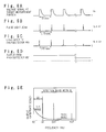
- Figs. 6A to 6D and 6E are views for explaining the operation of the 1st comparative apparatus.
- Figs. 6A to 6D are timing charts of signals at the respective positions.
- Fig. 6E is a graph showing the detection frequency band width.
- This pulse light beam is linearly polarized by the PBS 841, optically biased by the wave plate 842, focused by the objective lens 843, and input to the E-O probe 844.
- the polarized state of the light beam passing through the E-O probe 844 changes accordingly.
- the pulse light beam incident on the E-O probe 844 is reflected by the bottom surface of the E-O probe 844 and input to the PBS 841 again through the objective lens 843 and the wave plate 842. Only a component of the polarization direction perpendicular to the polarization direction of the light beam previously output from the PBS 841 is reflected.
- the light beam input to the PBS 841 again is optically biased by the wave plate 842 twice, as compared to the light beam previously output from the PBS.
- the intensity of the light beam input to the photodetection unit 850 changes in accordance with the polarized state changed through the E-O probe 844.
- the light beam passing through the wave plate 842 twice is optically biased by ⁇ /4 in the polarization direction. Therefore, if no voltage is generated at the target measurement portion, the 1/2 light beam reflected by the E-O probe 844 is input to the photodetection unit 850.
- the repetition frequency f 0 + ⁇ f of the probe light beam differs from the fundamental frequency f 0 of the voltage signal generated at the target measurement portion.
- the measurement device 860 receives the detection signal of the beat signal output from the photodetection unit 850, subtracts a DC component, and displays the measurement result on the display unit 870.
- a relatively low frequency lower than 1 kHz is normally applied as the beat frequency ⁇ f, i.e., the measurement frequency.
- ⁇ f the beat frequency
- 1/f noise is large, so no high signal-to-noise ratio (S/N ratio) can be obtained.
- Fig. 7 is a block diagram showing the arrangement of the 2nd comparative apparatus. As shown in Fig.
- the 2nd comparative apparatus operates as that of the 1st comparative apparatus to perform measurement while increasing the measurement frequency close to the modulation frequency f M by using a polarization light modulation method. More specifically, a light beam output from the pulse light source 910 generates a component of a frequency f 1 + f M through the optical modulator 922. An optical signal having a component of a frequency
- Fig. 8 is a graph for explaining reduction of 1/f noise in measurement by the 2nd comparative apparatus. As shown in Fig. 8, in the 2nd comparative apparatus, an optical signal is measured while reducing 1/f noise almost to shot noise.
- the present invention has been made in consideration of the above situation, and has as its object to provide a voltage measurement apparatus for accurately measuring a voltage.
- a voltage measurement apparatus characterized in that the apparatus is brought close to or into contact with a target measurement portion of a sample to be measured to detect a voltage of the target measurement portion, and comprises (a) a light source for emitting a light beam intensity-modulated at an externally designated first frequency, (b) a polarizer for receiving the light beam emitted from the light source, selecting a component of a first polarization direction, and outputting the component as a probe light beam, (c) a first optical system for applying an optical bias associated with a polarized state to the probe light beam output from the polarizer and guiding the probe light beam to the target measurement portion, (d) an electro-optic conversion probe (E-O probe) having a member which is arranged at a position in contact with or close to the target measurement portion and consists of an electro-optic material having an electro-optic effect, the member having a reflection-processed bottom surface on the target measurement portion side, (e) a drive unit for driving the
- the drive unit may comprise 1 a drive device for outputting a drive signal for driving the sample at the second frequency and outputting a trigger signal having the second frequency, 2 a frequency multiplier for receiving the trigger signal output from the drive device, receiving notification of the first number output from the processing unit, and generating a signal of the third frequency obtained by multiplying the second frequency by the first number, 3 an oscillator for generating the signal of the fourth frequency, and 4 a light source modulator for receiving the signal output from the frequency multiplier and the signal output from the oscillator to generate the signal of the first frequency corresponding to a sum of a value of the third frequency and a value of the fourth frequency, and notifying the light source of the signal.
- a two-dimensional photodetector can be used as the photodetector.
- the synchronous detection unit may comprise 1 a filter for receiving the photodetection signal output from the photodetector and selecting the component of the fourth frequency, and 2 a synchronous detector for receiving the signal output from the filter and the signal of the fourth frequency output from the drive unit and detecting the signal output from the filter in synchronism with the signal of the fourth frequency output from the drive unit.
- the synchronous detection signals are 1 an amplitude detection signal representing an amplitude of the component of the fourth frequency of the photodetection signal output from the photodetector, and 2 a phase detection signal representing a phase difference between the amplitude detection signal representing the component of the fourth frequency of the photodetection signal output from the photodetector and the signal of the fourth frequency output from the drive unit, and the processing unit notifies the drive unit of the first number while sequentially changing the first number by one, acquires the amplitude detection signal and the phase detection signal at the time of notification of the first number every time the first number is notified, and calculates a time waveform of a voltage signal generated at the target measurement portion by the drive signal in accordance with calculation of Fourier transform upon completion of acquisition.
- the drive unit supplies a drive signal of the frequency f 0 to the sample and supplies a modulation signal of a frequency N ⁇ f 0 + ⁇ f to the light source.
- the sum frequency N ⁇ f 0 + ⁇ f will be described below, though a difference frequency N ⁇ f 0 - ⁇ f may also be used.
- an intensity-modulated light beam is emitted from the light source and incident on the E-O probe sequentially through the polarizer and the first optical system.
- a periodical voltage waveform is generated at the target measurement portion near the arrangement position of the E-O probe at the fundamental period 1/f 0 .
- 0, 1,.8) This photodetection signal is input to the synchronous detection unit, and the component of the frequency ⁇ f is heterodyne-detected.
- the synchronous detection signal is acquired and stored as data corresponding to each designated number N. Acquisition and storing are continued until the designated number N for allowing the value of the synchronous detection signal to be regarded as almost zero is reached.
- the arithmetic unit Upon completion of acquisition and storing, the arithmetic unit reproduces the waveform of the voltage signal generated at the target measurement portion by calculation of Fourier transform on the basis of the stored data and displays the waveform.
- the heterodyne detection method of the apparatus of the present invention substantially differs from that of the 1st comparative apparatus. More specifically, in the heterodyne detection method of the 1st comparative apparatus, the detection band width must be set in a wide range up to n ⁇ f. However, in the apparatus of the present invention, only the component of ⁇ f is measured so that a very narrow band width can be set.
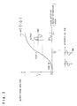
- Fig. 1 is a block diagram showing the arrangement of a voltage measurement apparatus according to the first embodiment of the present invention.
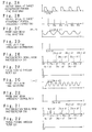
- Figs. 2A to 2J are charts for explaining the operation of the voltage measurement apparatus according to the first embodiment of the present invention.
- Fig. 3 is a graph for explaining an optical bias.
- Fig. 4 is a block diagram showing the arrangement of a voltage measurement apparatus according to the second embodiment of the present invention.
- Fig. 5 is a block diagram showing the arrangement of the 1st comparative apparatus.
- Figs. 6A to 6E are views for explaining the operation of the 1st comparative apparatus.
- Fig. 7 is a block diagram showing the arrangement of the 2nd comparative apparatus.
- Fig. 8 is a graph for explaining the operation of the 2nd comparative apparatus.
- Fig. 1 is a block diagram showing the arrangement of a voltage measurement apparatus according to the first embodiment of the present invention.
- the apparatus of this embodiment comprises (a) a light source 110 for generating an intensity-modulated light beam when a modulation frequency N ⁇ f 0 + ⁇ f is externally notified, (b) a polarization beam splitter (PBS) 120 for receiving the light beam emitted from the light source 110, selecting a component of the first polarization direction (X direction in Fig. 1), outputting the component as a probe light beam, and reflecting a light beam of the second polarization direction (Y direction in Fig.
- PBS polarization beam splitter
- the drive unit 300 has 1 a drive device 310 for outputting a drive signal for driving the sample 700 at the frequency f 0 , and outputting a trigger signal having the frequency f 0 , 2 a frequency multiplier 320 for receiving the trigger signal output from the drive device 310, and receiving the notification of the designated number N output from the processing unit 600 to generate a signal of the frequency N ⁇ f 0 obtained by multiplying the designated number N by the frequency f 0 , 3 an oscillator 330 for generating the signal of the frequency ⁇ f 0 , and 4 a light source modulator 340 for receiving the signal output from the frequency multiplier 320 and the signal output from the oscillator 330, and generating a signal of the frequency N ⁇ f 0 + ⁇ f corresponding to the sum of the frequency N ⁇ f 0 and the frequency ⁇ f, and outputting the signal to the light source 110.
- the light source modulator 340 has 1 a frequency mixer 341, and 2 a capacitor C arranged at the output stage of the frequency mixer 34
- the synchronous detection unit 520 has 1 a filter 521 for receiving the photodetection signal output from the photodetector 510 and selecting the component of the frequency ⁇ f, and 2 a synchronous detector 522 for receiving the signal output from the filter 521 and the signal of the frequency ⁇ f output from the drive unit 300, detecting the signal output from the filter 521 in synchronism with the signal of the frequency ⁇ f output from the drive unit 300, and outputting i) an amplitude detection signal representing the amplitude of the component of the frequency ⁇ f of the photodetection signal output from the photodetector 510, and ii) a phase detection signal representing the phase difference between the signal of the component of the frequency ⁇ f of the photodetection signal output from the photodetector 510 and the signal of the frequency ⁇ f output from the drive unit.
- a narrow-band detector such as a network analyzer, a spectrum analyzer, and a lock-in amplifier can be preferably employed.
- the apparatus of this embodiment measures a voltage signal waveform at the target measurement position 710 of the sample 700 in the following manner.
- Figs. 2A to 2H are charts showing the operation of the apparatus of this embodiment.
- the drive unit 300 supplies a drive signal of the frequency f 0 to the sample 700 and supplies a modulation signal of the frequency N ⁇ f 0 + ⁇ f to the light source 110.
- an intensity-modulated light beam is emitted from the light source 110 and incident on the E-O probe 200 through the PBS 120, the wave plate 130, and the objective lens 140.
- a periodical voltage waveform is generated at the target measurement portion near the arrangement position of the E-O probe 200 at a fundamental period 1/f 0 .
- Fig. 3 is a graph for explaining the optical bias applied by the wave plate.
- a 1/4 wave plate is used to set the optical bias to a point A in Fig. 3. With this setting, the maximum output change can be obtained with respect to the output from the analyzer 422. In this case, however, a DC output as large as I 1 /2 is also output together with the modulation output, and shot noise is generated due to this DC output.
- the wave plate 421 may be selected to optimize the optical bias, thereby obtaining a satisfactory S/N ratio.
- 0, 1,.8)
- This photodetection signal is input to the synchronous detection unit 520, and the component of the frequency ⁇ f is heterodyne-detected.
- the synchronous detection signal is acquired and stored as data corresponding to each designated number N. Acquisition and storing are continued until the designated number N for allowing the value of the synchronous detection signal to be regarded as almost zero is reached, or until the limit frequency for the modulation capability of the light source 110 is reached.
- the arithmetic unit 610 of the processing unit 600 Upon completion of acquisition and storing, the arithmetic unit 610 of the processing unit 600 reproduces the waveform of the voltage signal generated at the target measurement portion by calculation of Fourier transform on the basis of the stored data and displays the reproduction result on a display unit 620.
- Fig. 4 is a block diagram showing the arrangement of a voltage measurement apparatus according to the second embodiment of the present invention.
- the apparatus of this embodiment measures the two-dimensional voltage distribution of a target measurement portion.
- the apparatus of this embodiment differs from that of the first embodiment in that a collimator lens 113 and a collimator lens 141 are arranged between a light source 110 and a PBS 120 and between a focusing lens 140 and an E-O probe 200, respectively, to form an imaging optical system, an imaging system 150 consisting of a lens 151 and a lens 152 is arranged between the PBS 120 and a photodetector 510, and a two-dimensional photodetector 550 is employed as a photodetector.
- a processing unit a processing unit 650 having an arithmetic unit 651 is employed.
- a high-speed read CCD image sensor capable of performing a high-speed read operation is used.
- a general two-dimensional photodetector such as a photodiode array, an imaging tube, a normal CCD image sensor, or a linear array sensor can also be used.
- an intensity-modulated light beam emitted from the light source 110 is collimated and incident on the E-O probe 200, and reflected.
- the two-dimensional image of the reflecting portion is formed, input to the two-dimensional photodetector 550, and converted to a two-dimensional photodetection signal.
- the processing unit 650 acquires and stores a synchronous detection signal at each measurement point, and reproduces the voltage waveform at each measurement point upon completion of acquisition and storing.
- an intensity-modulated light beam is employed, and after the intensity-modulated light beam is influenced by the voltage generated in the sample, modulation and heterodyne detection are performed. Therefore, an accurate voltage measurement apparatus which has a wide frequency band width and needs no short-pulse light source can be realized.
Landscapes
- Physics & Mathematics (AREA)
- General Physics & Mathematics (AREA)
- Measurement Of Current Or Voltage (AREA)
- Tests Of Electronic Circuits (AREA)
- Measuring Instrument Details And Bridges, And Automatic Balancing Devices (AREA)
- Investigating Or Analysing Materials By Optical Means (AREA)
Applications Claiming Priority (2)
| Application Number | Priority Date | Filing Date | Title |
|---|---|---|---|
| JP01925895A JP3500216B2 (ja) | 1995-02-07 | 1995-02-07 | 電圧測定装置 |
| JP19258/95 | 1995-02-07 |
Publications (2)
| Publication Number | Publication Date |
|---|---|
| EP0726471A2 true EP0726471A2 (de) | 1996-08-14 |
| EP0726471A3 EP0726471A3 (de) | 1997-02-26 |
Family
ID=11994414
Family Applications (1)
| Application Number | Title | Priority Date | Filing Date |
|---|---|---|---|
| EP96300811A Withdrawn EP0726471A3 (de) | 1995-02-07 | 1996-02-07 | Elektrooptische Spannungsmessvorrichtung |
Country Status (3)
| Country | Link |
|---|---|
| US (1) | US5767688A (de) |
| EP (1) | EP0726471A3 (de) |
| JP (1) | JP3500216B2 (de) |
Cited By (3)
| Publication number | Priority date | Publication date | Assignee | Title |
|---|---|---|---|---|
| WO2005096004A1 (en) * | 2004-03-05 | 2005-10-13 | Qc Solutions, Inc. | Real-time in-line testing of semiconductor wafers |
| US7160742B2 (en) | 2003-07-21 | 2007-01-09 | Qc Solutions, Inc. | Methods for integrated implant monitoring |
| FR3013122A1 (fr) * | 2013-11-12 | 2015-05-15 | Centre Nat Etd Spatiales | Procede et dispositif d'extraction d'une forme d'onde a basse frequence d'un composant electro-optique |
Families Citing this family (15)
| Publication number | Priority date | Publication date | Assignee | Title |
|---|---|---|---|---|
| US6057677A (en) * | 1996-04-24 | 2000-05-02 | Fujitsu Limited | Electrooptic voltage waveform measuring method and apparatus |
| WO2000024207A1 (en) * | 1998-10-19 | 2000-04-27 | Dori, Eli | Service providers localization system via cellular telephone |
| JP2000162243A (ja) * | 1998-11-30 | 2000-06-16 | Ando Electric Co Ltd | 電気光学サンプリングプローバ |
| JP2000241510A (ja) * | 1999-02-24 | 2000-09-08 | Ando Electric Co Ltd | 集積回路テスタ |
| US6337565B1 (en) | 1999-03-25 | 2002-01-08 | Ando Electric Co., Ltd. | Electro-optic probe |
| US6714000B2 (en) * | 1999-06-14 | 2004-03-30 | Genscape, Inc. | Method for monitoring power and current flow |
| JP5119523B2 (ja) * | 2005-01-12 | 2013-01-16 | 独立行政法人情報通信研究機構 | 近傍電磁界測定装置 |
| US7733100B2 (en) | 2005-08-26 | 2010-06-08 | Dcg Systems, Inc. | System and method for modulation mapping |
| JP2008020305A (ja) * | 2006-07-12 | 2008-01-31 | National Institute Of Information & Communication Technology | 電磁界高速撮像装置 |
| JP5084006B2 (ja) * | 2006-07-12 | 2012-11-28 | 独立行政法人情報通信研究機構 | 電磁界高速撮像装置 |
| FR2906039B1 (fr) * | 2006-09-20 | 2009-01-23 | Univ Paris Sud Etablissement P | Procede et dispositif pour caracteriser un signal electrique se propageant dans un echantillon. |
| SG10201401887YA (en) | 2009-05-01 | 2014-06-27 | Dcg Systems Inc | Systems and method for laser voltage imaging state mapping |
| WO2014119676A1 (ja) | 2013-02-01 | 2014-08-07 | 浜松ホトニクス株式会社 | 半導体デバイス検査装置及び半導体デバイス検査方法 |
| JP6283501B2 (ja) * | 2013-11-12 | 2018-02-21 | 浜松ホトニクス株式会社 | 周波数解析装置及び周波数解析方法 |
| JP2019211424A (ja) * | 2018-06-08 | 2019-12-12 | 国立研究開発法人情報通信研究機構 | イメージング装置 |
Family Cites Families (8)
| Publication number | Priority date | Publication date | Assignee | Title |
|---|---|---|---|---|
| US4446425A (en) * | 1982-02-12 | 1984-05-01 | The University Of Rochester | Measurement of electrical signals with picosecond resolution |
| US4618819A (en) * | 1984-03-27 | 1986-10-21 | The University Of Rochester | Measurement of electrical signals with subpicosecond resolution |
| DE3889986T2 (de) * | 1987-07-13 | 1994-09-15 | Hamamatsu Photonics Kk | Anordnung eines Spannungsdetektors. |
| US4891580A (en) * | 1988-04-29 | 1990-01-02 | American Telephone And Telegraph Co., At&T Bell Laboratories | Electro-optic measurements of voltage waveforms on electrical conductors |
| DE3924369A1 (de) * | 1989-07-22 | 1991-01-31 | Asea Brown Boveri | Verfahren zur messung eines elektrischen feldes oder einer elektrischen spannung und einrichtung zur durchfuehrung des verfahrens |
| GB8921458D0 (en) * | 1989-09-22 | 1989-11-08 | Univ Strathclyde | Cell culture apparatus |
| JP2742473B2 (ja) * | 1991-03-26 | 1998-04-22 | 浜松ホトニクス株式会社 | 高速電圧測定装置 |
| JPH06102295A (ja) * | 1992-07-28 | 1994-04-15 | Hewlett Packard Co <Hp> | 非接触型プローブおよび非接触電圧測定装置 |
-
1995
- 1995-02-07 JP JP01925895A patent/JP3500216B2/ja not_active Expired - Fee Related
-
1996
- 1996-02-06 US US08/597,267 patent/US5767688A/en not_active Expired - Fee Related
- 1996-02-07 EP EP96300811A patent/EP0726471A3/de not_active Withdrawn
Cited By (5)
| Publication number | Priority date | Publication date | Assignee | Title |
|---|---|---|---|---|
| US7160742B2 (en) | 2003-07-21 | 2007-01-09 | Qc Solutions, Inc. | Methods for integrated implant monitoring |
| WO2005096004A1 (en) * | 2004-03-05 | 2005-10-13 | Qc Solutions, Inc. | Real-time in-line testing of semiconductor wafers |
| US7119569B2 (en) | 2004-03-05 | 2006-10-10 | Qc Solutions, Inc. | Real-time in-line testing of semiconductor wafers |
| FR3013122A1 (fr) * | 2013-11-12 | 2015-05-15 | Centre Nat Etd Spatiales | Procede et dispositif d'extraction d'une forme d'onde a basse frequence d'un composant electro-optique |
| WO2015071582A1 (fr) * | 2013-11-12 | 2015-05-21 | Centre National D'Études Spatiales C N E S | Procédé et dispositif d'extraction d'une forme d'onde à basse fréquence d'un composant électro-optique |
Also Published As
| Publication number | Publication date |
|---|---|
| JPH08211132A (ja) | 1996-08-20 |
| EP0726471A3 (de) | 1997-02-26 |
| JP3500216B2 (ja) | 2004-02-23 |
| US5767688A (en) | 1998-06-16 |
Similar Documents
| Publication | Publication Date | Title |
|---|---|---|
| US5767688A (en) | Electro-optic voltage measurement apparatus | |
| JP3364333B2 (ja) | 減衰特性測定装置 | |
| US6876441B2 (en) | Optical sensor for distance measurement | |
| EP0460696A2 (de) | Rauscharme Laserdioden-Pulslichtquelle und Spannungsdetektor unter Verwendung derselben rauscharmen Laserdioden-Pulslichtquelle | |
| KR900003116B1 (ko) | 단차계측장치 | |
| JPH112667A (ja) | Icのデュアルレーザ電圧プロービング | |
| JP2004527765A5 (de) | ||
| KR20010104199A (ko) | 집적 회로의 차분 펄스 레이저 빔 검사 | |
| US5153667A (en) | Apparatus for detecting the change of light intensity | |
| US4975635A (en) | Voltage detector using a sampling type high-speed photodetector | |
| US5666062A (en) | Voltage measuring using electro-optic material's change in refractive index | |
| EP1645854A1 (de) | Verfahren und Vorrichtung zur Bestimmung der Linearität eines optischen Detektors | |
| US6958817B1 (en) | Method of interferometry with modulated optical path-length difference and interferometer | |
| US5847570A (en) | Low jitter trigger circuit for electro-optic probing apparatus | |
| US5625296A (en) | Electro-optic voltage measurement apparatus | |
| JP3352543B2 (ja) | 電圧測定装置 | |
| JP3352244B2 (ja) | 電圧測定装置 | |
| JP3165873B2 (ja) | 電気信号測定方法および装置 | |
| JPH11287859A (ja) | レーザ距離計 | |
| JP2734786B2 (ja) | 光エコー顕微鏡 | |
| US7218402B1 (en) | Wavefront sensor using hybrid optical/electronic heterodyne techniques | |
| JP3236941B2 (ja) | 光波距離計における測距方法 | |
| JPS6371675A (ja) | レ−ザ−測距装置 | |
| JP2002031658A (ja) | 高周波電磁波検出システム及び高周波電磁波検出方法 | |
| EP0307936B1 (de) | Vielkanalspannungsdetektor |
Legal Events
| Date | Code | Title | Description |
|---|---|---|---|
| PUAI | Public reference made under article 153(3) epc to a published international application that has entered the european phase |
Free format text: ORIGINAL CODE: 0009012 |
|
| AK | Designated contracting states |
Kind code of ref document: A2 Designated state(s): DE FR GB |
|
| PUAL | Search report despatched |
Free format text: ORIGINAL CODE: 0009013 |
|
| AK | Designated contracting states |
Kind code of ref document: A3 Designated state(s): DE FR GB |
|
| 17P | Request for examination filed |
Effective date: 19970822 |
|
| 17Q | First examination report despatched |
Effective date: 20010702 |
|
| STAA | Information on the status of an ep patent application or granted ep patent |
Free format text: STATUS: THE APPLICATION IS DEEMED TO BE WITHDRAWN |
|
| 18D | Application deemed to be withdrawn |
Effective date: 20011113 |