EP0460696A2 - Rauscharme Laserdioden-Pulslichtquelle und Spannungsdetektor unter Verwendung derselben rauscharmen Laserdioden-Pulslichtquelle - Google Patents
Rauscharme Laserdioden-Pulslichtquelle und Spannungsdetektor unter Verwendung derselben rauscharmen Laserdioden-Pulslichtquelle Download PDFInfo
- Publication number
- EP0460696A2 EP0460696A2 EP91109352A EP91109352A EP0460696A2 EP 0460696 A2 EP0460696 A2 EP 0460696A2 EP 91109352 A EP91109352 A EP 91109352A EP 91109352 A EP91109352 A EP 91109352A EP 0460696 A2 EP0460696 A2 EP 0460696A2
- Authority
- EP
- European Patent Office
- Prior art keywords
- pulsed light
- electrooptic material
- laser diode
- light source
- low noise
- Prior art date
- Legal status (The legal status is an assumption and is not a legal conclusion. Google has not performed a legal analysis and makes no representation as to the accuracy of the status listed.)
- Withdrawn
Links
Images


Classifications
-
- G—PHYSICS
- G01—MEASURING; TESTING
- G01R—MEASURING ELECTRIC VARIABLES; MEASURING MAGNETIC VARIABLES
- G01R15/00—Details of measuring arrangements of the types provided for in groups G01R17/00 - G01R29/00, G01R33/00 - G01R33/26 or G01R35/00
- G01R15/14—Adaptations providing voltage or current isolation, e.g. for high-voltage or high-current networks
- G01R15/22—Adaptations providing voltage or current isolation, e.g. for high-voltage or high-current networks using light-emitting devices, e.g. LED, optocouplers
-
- H—ELECTRICITY
- H01—ELECTRIC ELEMENTS
- H01S—DEVICES USING THE PROCESS OF LIGHT AMPLIFICATION BY STIMULATED EMISSION OF RADIATION [LASER] TO AMPLIFY OR GENERATE LIGHT; DEVICES USING STIMULATED EMISSION OF ELECTROMAGNETIC RADIATION IN WAVE RANGES OTHER THAN OPTICAL
- H01S5/00—Semiconductor lasers
- H01S5/06—Arrangements for controlling the laser output parameters, e.g. by operating on the active medium
- H01S5/068—Stabilisation of laser output parameters
- H01S5/0683—Stabilisation of laser output parameters by monitoring the optical output parameters
- H01S5/06835—Stabilising during pulse modulation or generation
-
- H—ELECTRICITY
- H01—ELECTRIC ELEMENTS
- H01S—DEVICES USING THE PROCESS OF LIGHT AMPLIFICATION BY STIMULATED EMISSION OF RADIATION [LASER] TO AMPLIFY OR GENERATE LIGHT; DEVICES USING STIMULATED EMISSION OF ELECTROMAGNETIC RADIATION IN WAVE RANGES OTHER THAN OPTICAL
- H01S5/00—Semiconductor lasers
- H01S5/06—Arrangements for controlling the laser output parameters, e.g. by operating on the active medium
- H01S5/062—Arrangements for controlling the laser output parameters, e.g. by operating on the active medium by varying the potential of the electrodes
- H01S5/06209—Arrangements for controlling the laser output parameters, e.g. by operating on the active medium by varying the potential of the electrodes in single-section lasers
- H01S5/06216—Pulse modulation or generation
Definitions
- the present invention relates to a pulsed light source utilizing a laser diode for generating a short pulsed light of a high repetitive frequency (200 to 2 picosecond pulse width, for example), and more specifically to a low noise pulsed light source capable of generating an optical pulse with reduced light intensity noise and to a voltage detector device utilizing the same low noise pulsed light source.
- An emitted light from a laser diode changes in its wavelength and intensity as an excitation current and ambient temperature vary.
- the intensity of the emitted light also changes owing to the competition among longitudinal modes and owing to mode hopping.
- a photodetector element such as a photodiode (PD) detects part of the emitted light from a laser diode to estimate an error signal between a detected light intensity level and a preset one which is in turn fed back to an excitation current source which is to drive the laser diode.
- PD photodiode
- a dye laser which generates a picosecond to femtosecond width pulsed light is usable for such applications from the viewpoint of temporal resolution but with a difficulty of its being large-sized. Instead of this, laser diodes are hopeful as pulsed light sources, because they have some advantages of their being simple and small-sized instructure, inexpensive in manufacture.
- laser diodes can generate a short pulsed light with an about 200 to 20 picosecond width, and with about 670 nm to 1.5 ⁇ m wavelengths in typical, the latter emission wavelengths being varied depending upon the kinds thereof.
- a second harmonic of the pulsed light from a laser diode is available to assure a short wavelength pulsed light up to 340 nm.
- Repetitive frequencies of such optical pulses generally range from 0.1 to 200 MHz although being different in accordance with applications.
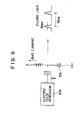
- a laser diode 12A (refer to Fig. 9) incorporated in a laser diode (LD) pulsed light source 12 emits the optical pulse which is controlled in its repetitive frequency by an oscillator 14 (repetitive frequency 100 MHz, pulse width 50 picosecond, and wavelength 830 nm, for example).
- the LD pulsed light source 12 is constructed as illustrated in Fig.
- the pulsed light emitted from the laser diode (LD) 12A impinges upon the sample 10 through a chopper 16 (chopping frequency 1 kHz, for example) driven by the oscillator 15 and is partly absorbed by and partly transmitted through the same as an output light.
- the output light is focused by a lens 18 and detected by a photodetector 20 composed of a photodiode (PD) for example.
- An output signal from the photodetector 20 is amplified by a low noise amplifier 22 and lock-in detected by a lock-in amplifier 24.
- a chopper signal generated by the oscillator 15 is used for a reference signal in the lock-in amplifier 24.
- noises produced in the photodetector 20 and in the low noise amplifier 22 have sufficiently been more reduced than that involved in the transmitted light.
- An output from the lock-in amplifier 24 is fed to an output meter 26 for example and displayed with respect to the transmittance of the foregoing output light.
- the incident pulsed light in case where the transmittance of the pulsed light through the sample 10 is nonlinear with respect to the incident pulsed light, the incident pulsed light must be measured up to a sufficiently low level of the intensity thereof. Thereupon, a difficulty is produced of noise involved in the pulsed light emitted from a pulsed oscillation LD, which limits the lower boundary of the measurement.
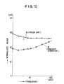
- exemplary noise characteristics of the LD pulsed light obtained experimentally by the present inventors are illustrated, with the horizontal axis taking frequencies and the vertical axis effective values (rms) of photoelectric current noise in decibel (dB).
- the point O dB on the vertical axis indicates a short noise level defined by the square root of the number of photons involved in the optical pulse (theoretical limit).
- Fig. 10 therefore indicates a noise level of the LD pulsed light normalized by the shot noise level.
- Fig. 10 further illustrates a noise level with the prior system as indicated by a solid line A and marks X. It is understood from the figure that the noise level when the LD undergoes pulsed oscillation is greater 10 times (20 dB) or more than the shot noise level, so that the former may be reduced to the latter shot noise level.
- the data illustrated in Fig. 10 is given by measuring involved noise produced when the LD 12A to be measured is driven by a driving circuit 30 constructed as illustrated in Fig. 9 using a noise fraction measuring device composed of the photodetector 20, low noise amplifier 22, lock-in amplifier 24, an oscillator (OSC) 32 for frequency sweep, a noise detection circuit 34, and a display 36.
- a noise fraction measuring device composed of the photodetector 20, low noise amplifier 22, lock-in amplifier 24, an oscillator (OSC) 32 for frequency sweep, a noise detection circuit 34, and a display 36.
- Another object of the present invention is to provide a device for measuring voltage highly accurately utilizing an electrooptic effect with use of such a low noise pulsed light source as described above.
- a low noise pulsed light source utilizing a laser diode characterized in that said light source comprises a laser diode for emitting repetitive pulsed light, an electric pulse generator for driving said laser diode, a current source for supplying a bias current to said laser diode, a photodetector for detecting part of the pulsed light emitted from said laser diode, a control means for modulating at least one of the bias current from said current sources and the amplitude of a pulse signal generated from said electric pulse generator in accordance with an output signal from said photodetector over a wide frequency band such that the intensity of said pulsed light is kept unchanged and any noise superimposed on said intensity of said pulsed light is reduced; and in that a feedback system including the photodetector and the control means has a peak in its frequency characteristics with in a frequency band for light detecting in a light measuring system utilizing the low noise pulsed light source.
- a low noise pulsed light source utilizing a laser diode characterized in that the light measuring system includes a lock-in-amplifier lock-in amplifying a detected signal, and the frequency band for light detecting is the lock-in-frequency of the lock-in-amplifier.
- the bias current from said current source is modulated and controlled in a frequency band below a predetermined frequency while the amplitude of a pulse signal generated by said electric pulse generator is modulated and controlled in a frequency band above the predetermined frequency in accordance with an output signal from said photodetector such that intensity of the pulsed light remains unchanged and any light intensity noise is reduced.
- said electric pulse generator incorporates a stem recovery diode.
- said optical detector is assembled together with a laser diode as a set in the same package.
- the time constant of a feedback system which detect the pulsed light and controls the same is longer than the repetitive period of the pulsed light.
- the frequency characteristics of the feedback system has a peak to reduce involved noise in a specific frequency range, and the frequency of a reference signal of a lock-in amplifier for use in a measuring system falls within said specific frequency range.
- a voltage detector device of such a type as those utilizing an electrooptic material which has its refractive index varied by voltage of a predetermined portion of an object to be measured is applied and is characterized in including a first electrooptic material influenced by the voltage of a predetermined portion of the object, a second electrooptic material disposed to compensate a phase difference caused by spontaneous double refraction of said first electrooptic material, and the low noise pulsed light source a low noise pulsed light source utilizing a laser diode comprising a laser diode for emitting repetitive pulsed light, an electric pulse generator for driving said laser diode, a current source for supplying a bias current to said laser diode, a photodetector for detecting part of the pulsed light emitted from said laser diode, and a control means for modulating at least one of the bias current from said current sources and the amplitude of a pulse signal generated from said electric pulse generator in accordance with an output signal from said photodetector over a wide
- said second electrooptic material is disposed in its optical crystal axis to be perpendicular to the optical crystal axis of said first electrooptic material.
- said second electrooptic material is disposed in its optical crystal axis to be parallel to the optical crystal axis of said first electrooptic material, and means is provided between said first and second electrooptic materials for rotating by 90° the polarization component of the light.
- the device is further provided with a first transparent electrode provided between said first and second electrooptic materials, and a second transparent electrode provided oppositely to the side where said first transparent electrode of said second electrooptic material.
- said first transparent electrode is kept at around potential, and voltage is applied to said second transparent electrode to output light from the same, said light is such that produced by removing a DC component from the polarization state of exit light from said second electrooptic material.
- a voltage detector of such a type a those utilizing an electrooptic material which has its refractive index changed by voltage of a predetermined portion of an object to be measured is applied, in which said electrooptic material is positioned at a predetermined location in an optical probe, which material includes at the tip end thereof reflecting means for reflecting an optical beam incident along the center axis of said optical probe and further includes a transparent electrode oppositely to the side where said reflecting means of the electrooptic material is provided, and said optical beam is pulsed light emitted from a low noise pulsed light source utilizing a laser diode comprising a laser diode for emitting repetitive pulsed light, an electric pulse generator for driving said laser diode, a current source for supplying a bias current to said laser diode, a photodetector for detecting part of the pulsed light emitted from said laser diode, and a control means for modulating at least one of the bias current from said current sources and the amplitude of a pulse signal generated from said electric pulse generator
- said transparent electrode is set in its surface to be perpendicular to the center axis of said optical probe.
- a voltage detector of such a type as those utilizing an electrooptic material which has its refractive index changed by applying voltage of a predetermined portion of an object to be measured in which said detector includes a low noise pulsed light source utilizing a laser diode comprising a laser diode for emitting repetitive pulsed light, an electric pulse generator for driving said laser diode, a current source for supplying a bias current to said laser diode, a photodetector for detecting part of the pulsed light emitted from said laser diode, and a control means for modulating at least one of the bias current from said current sources and the amplitude of a pulse signal generated from said electric pulse generator in accordance with an output signal from said photodetector over a wide frequency band such that the intensity of said pulsed light is kept unchanged and any noise superimposed on said intensity of said pulsed light is reduced, said electrooptic material being positioned to cover therewith a plurality of measurement positions of the object from which voltage is to be detected, the pulse
- each of incident lights which are yielded by dividing the optical beam from the low noise pulsed light source to many desired patterns, enters each of specific portions of said electrooptic material corresponding to specific portions of the object.
- an optical beam emanating from the light source is divided to many incident lights of each of grid-shaped patterns through a micro-lens array.
- said electrooptic material being positioned so as to cover therewith a plurality of two-dimensional positions of an object from which voltage is to be detected, the optical beam from said low noise pulsed light source entering uniformly parallely the respective two-dimensional portions of said electrooptic material corresponding to the plurality of the two-dimensional positions of the object, changes in polarization states of exit lights from the plurality of the two-dimensional portions of said electrooptic material being detected by detectors.
- said electrooptic material being positioned so as to cover therewith a plurality of two-dimensional positions of an object from which voltage is to be detected, an optical beam with a short pulse duration from said low noise pulsed light source entering uniformly parallely respective two-dimensional portions of said electrooptic material corresponding to the plurality of the two-dimensional positions of the object, chances polarization states of exit lights from the plurality of the two-dimensional portions of said electrooptic material being detected by detectors, and in which said voltage detector further includes an observation light source for outputting an optical beam with a wavelength different from that from said low noise pulsed light source, said optical beam being used for observation of the wiring arrangement of the object, switching means for switching the optical beams from said observation light source and from said low noise pulsed light to direct the switched optical beam to said electrooptic material, phase compensator means for adjusting, upon observation of the wiring arrangement of the object, the phase of exit light different from that upon detecting the change in said polarization state, display means for displaying thereon the voltages at the two-dimensional positions
- Fig. 1 illustrates an example of the basic construction of the first invention.
- a laser diode (LD) 38 is first brought to pulsed oscillation by previously supplying a bias current thereto and applying a short pulse electric signal thereto from an electric pulse generator 40 through a capacitor C1.
- a photodetector 42 such as a photodiode (PD) detects splitted light of the LD light or light emanating from the other end of the LD 38.
- An output from the photodetector 42 which is proportional to the intensity of the LD light is amplified and is used to permit a stabilized current modulator circuit 44 to modulate the bias current of the LD 38 over a wide frequency band and control the bias current such that the intensity of the LD light remains unchanged and any noise superimposed on the intensity of the pulsed light is reduced.
- the time constant of the feedback system is set to be sufficiently longer than the repetitive period of the LD pulsed light.
- the intensity of the LD pulsed light is automatically controlled to remain unchanged, and any noise involved in the LD light is also reduced as indicated by the broken line B and the marks ⁇ in Fig. 9.
- the foregoing stabilized current modulator circuit 44 is to compare the output from the optical detector 42 and a level signal, and includes, as shown in Fig. 2, a light intensity signal comparator circuit 44A for making constant a DC component such as a temperature change and temporal drift etc., involved in the light intensity, a light intensity noise extraction circuit 44B for extracting light intensity noise from an output signal of the optical detector 42 to stabilize an AC component such as a ripple that chances at light speed, and a stabilized current modulator circuit 44C for modulating a current on the basis of output signals from the light intensity signal comparator circuit 44A and the light intensity noise extraction circuit 44B.
- a light intensity signal comparator circuit 44A for making constant a DC component such as a temperature change and temporal drift etc., involved in the light intensity
- a light intensity noise extraction circuit 44B for extracting light intensity noise from an output signal of the optical detector 42 to stabilize an AC component such as a ripple that chances at light speed
- a stabilized current modulator circuit 44C for modulating a current on the
- the bias current supplied to the LD 38 was modulated by the stabilized current modulator circuit 44 over a wide frequency range in accordance with an output signal from the photodetector 42
- the construction to make constant the intensity of the LD pulsed light is not limited thereto.
- the electric pulse generator 40 may be replaced by the photodetector 42 and a stabilized electric pulse generator 41 as illustrated in Fig. 5, and the amplitude of a pulse signal generated by the stabilized electric pulse generator 41 may be modulates in accordance with an output signal from the photodetector 42.
- both may be combined such that the bias current is modulated by the stabilized current modulator circuit 44 in a frequency region below a predetermined frequency while the amplitude of a pulse signal generated by the stabilized electric pulse generator 41 is modulated in a frequency range above the predetermined frequency.
- An optical pulse generated by such the above LD is therefore usable for varieties of measuring fields such for example as E - O sampling, fluorescence lifetime measurement, estimation of response characteristics of photoelectric detector, OE ICs and the like, and temporal correlation photon counting.
- the above optical pulse improves the accuracy of those measurements and of the extension of the lower limits of the measurements, especially, is much effective by applying to a voltage detector.
- the second electrooptic material additionally to the first electrooptic material influenced by the voltage of a predetermined portion of an object to be measured, e.g., an integrated circuit, the second electrooptic material being disposed to compensate a phase difference caused by spontaneous double refraction of the first electrooptic material.
- the polarization state of the light is changed through the first electrooptic material oppositely to the case of the second electrooptic material owing to the phase difference by the spontaneous double refraction of the first electrooptic material, and further changed owing to the voltage of the predetermined portion of the object.
- the changes in the polarization states caused by the phase differences of the spontaneous double refraction of the first and second electrooptic materials are cancelled each other, resulting in the polarization state of the incident light being changed only by the voltage of the predetermined portion of the object.
- the first transparent electrode is interposed between the first and second electrooptic materials and is kept at earth potential for example.
- a second transparent electrode is disposed on the side of the second electrooptic material located oppositely to the side where the first transparent electrode of the second electrooptic material has been provided, to which electrode predetermined variable voltage for example is applied.
- the second electrooptic material compensates the influence of the phase change of the incident light due to the spontaneous double refraction in the first electrooptic material at all times.
- a DC component of the polarization state of the exit light from the first electrooptic material is eliminated by applying voltage to the second transparent electrode, and further the polarization state of the exit light from which the DC component has been eliminated, is compensated so as not to vary owing to a temperature change by making variable the voltage applied to the second transparent electrode following the temperature change.
- reflecting means such as a metal thin film, a dielectric multi-layer film mirror, and the like for example on the tip end of the electrooptic material, while there is provided the transparent electrode oppositely to the electrooptic material to the side of the same where said reflecting means has been provided.
- the surface of the transparent electrode is set to be perpendicular to the central axis of the optical probe for example and that the transparent electrode is kept at earth potential for example, and electric line of force produced by the voltage of the predetermined portion of the object is brought into a parallel one in the electrooptic material with respect to the central axis of the optical probe.
- the change in the refractive index of the electrooptic material is made uniform over the whole electrooptic material, so that the polarization state of the optical beam can be changed accurately corresponding to the voltage of the predetermined portion of the object.
- the electrooptic material is positioned so as to cover a plurality of measurement positions on an object from which voltages are to be detected, and an optical beam is directed to enter respective portions of the electrooptic material corresponding to the plurality of the measurement positions of the object for scanning over these respective portions.
- the optical beam may be deflected with the aid of a movable mirror, an acoustooptic deflector, and the like for example, or it may be realized by moving the electrooptic material and the object.
- voltages at the plurality of the measurement positions of the object can be detected with good operatability.
- the electrooptic material is positioned so as to cover a plurality of positions of an object, form which voltages are to be detected, and an optical beam from a light source is divided into many desired patterns by a microlens array, a holographic lens, or a spatial light modulator and directed to enter particular portions of the electrooptic material corresponding to the particular positions of the object.
- Refractive indexes of the respective portions of the electrooptic material are changed by the voltage at the respective positions of the object corresponding to the respective portions of the electrooptic material, so that the optical beam divided into many desired patterns and directed to enter the respective particular portions of the electrooptic material is changed in polarization states in conformity with the changes in the refractive indexes at the respective particular portions of the electrooptic material and emanating from the electrooptic material as an exit light to enter a detector, say, a two-dimensional photodetector array or a streak camera.
- the detector can detect the voltages at particular positions of the object, for example, the particular two-dimensional positions, simultaneously.
- the electrooptic material is positioned so as to cover a plurality of two-dimensional positions of an object, from which voltages are to be detected, and an optical beam from the light source is directed to enter respective two-dimensional portions of the electrooptic material corresponding to the plurality of the two-dimensional positions of the object.
- Refractive indexes of the respective two-dimensional port ions of the electrooptic material are changed owing the voltages at the respective two-dimensional positions of the object corresponding to the respective two-dimensional portions of the electrooptic material, so that the optical beam incident upon the respective two-dimensional portions of the electrooptic material is changed in its polarization states following the changes in the refractive indexes of the respective two-dimensional portions of the electrooptic material, emanating as exit light from the electrooptic material and directed to enter a detector, say, a two-dimensional photodetector array or a streak camera.
- the detector can detect the voltages at the two-dimensional positions on the object, simultaneously.
- the optical beam from the observation light source is first switched by the switching means to enter the electrooptic material for observation of the wiring configuration of the object, and the exit light is adjusted in its phase for observation by the phase compensator means.
- the optical beam from the observation light source enters the electrooptic material as parallel light and further enters the surface of the object after passing through the electrooptic material.
- the dielectric multi-layered film mirror on the bottom surface of the electrooptic material, which mirror is to transmit the optical beam from the observation light source therethrough but reflect the optical beam from the voltage detection light source thereon.
- the optical beam from the observation light source incident upon the surface of the object is partly reflected on the surface of the object is partly reflected on the surface of the object following the wiring configuration of the same to emanate from the electrooptic material as exit light.
- the exit light emanating from the electrooptic material is directed to enter a two-dimensional detector through the phase compensator means and is detected by the detector as visual image data of the wiring configuration of the object.
- the optical beam from the pulsed light source is switched by switching means to enter the electrooptic material for detecting the voltage at the two-dimensional positions of the object, and the exit light is adjusted in its phase for voltage detection by the phase compensator means.
- operation of the object is needed to be synchronized with the pulsed light.
- the display means displays the visual image data of the wiring configuration of the object detected by the detector on a display and the like together with the voltage distribution of the object in the one sampling timing superimposed on said visual image data.
- the optical beam from the pulsed light source is slightly delayed through the variable delay means, whereby the voltages at the two-dimensional positions of the object are detected in a timing slightly shifted from the previous sampling timing and displayed on the display means.
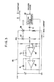
- a first embodiment of the present invention embodies the basic construction illustrated in Fig. 1 and principally comprises, as illustrated in Fig. 3, a reverse-biassed pin photodiode (PIN - PD) 43 for detecting part of emitted light from the LD 38, and a stabilized current modulator circuit 44 composed of a first amplifier 46 for inversely amplifying a photoelectric current signal yielded by the PIN - PD 43 to alter the DC level of an output signal and of a second amplifier 48 as an inverted current amplifier for inverting and amplifying the output of the first amplifier 46.
- PIN - PD reverse-biassed pin photodiode
- the first amplifier 46 has a feedback loop that incorporates a capacitor C2 for making longer the time constant of the first amplifier 46 than the repetitive period of the pulsed light.
- the second amplifier 48 has a feedback loop that incorporates a diode D for making zero the minimum of the bias current to prevent an opposite bias current from flowing.
- the intensity of pulsed light from the LD 38 is increased, for example, a photoelectric current from the PIN - PD 43 is increased to raise the potential at the point a in the figure.
- the output voltage of the first amplifier 46 is decreased, and hence the output current of the second amplifier 48 (the direction of the arrow in the figure is assumed to be positive) or the bias current is decreased. Therefore, the intensity of the output light from the LD 38 is reduced and controlled such that it remains unchanged.
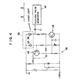
- the concrete construction of the first embodiment is exemplarily illustrated.
- the amplifiers 46, 48 comprise transistors, capacitors, and resistors, etc., respectively.
- a set of the LD 38 and the PIN - PD 38 is housed in the same package 50, for miniaturization thereof.
- a direct current (DC) bias current supplied from a current source 52 to the LD 38 is made constant, while a signal detected by the photodetector 42 is amplified by a photoelectric current amplifier 54 and adapted to modulate the amplitude of a pulse voltage applied from the stabilized electric pulse generator 41, that is controllable in amplitude over a wide frequency range, to the LD 38.
- DC direct current
- the stabilized electric pulse generator 41 comprises a light intensity signal comparator circuit 41A for comparing a signal from the amplifier 54 with a level signal to make constant a DC component such as a temperature chance and temporal drift, etc., involved in the intensity of the LD pulsed light, a light intensity noise extraction circuit 41B for stabilizing AC components, that change at high speed, such as ripples, etc., and an amplitude modulator circuit 41C for modulating the amplitude of an output pulse voltage on the basis of a signal which has been made constant in DC components thereof by the just-mentioned circuits and from which involved noise has been removed.
- a light intensity signal comparator circuit 41A for comparing a signal from the amplifier 54 with a level signal to make constant a DC component such as a temperature chance and temporal drift, etc., involved in the intensity of the LD pulsed light
- a light intensity noise extraction circuit 41B for stabilizing AC components, that change at high speed, such as ripples, etc.
- an amplitude modulator circuit 41C for modul
- the amplitude of the pulsed voltage is controlled such that it is reduced.
- the intensity of the LD pulsed light is kept unchanged and any involved noise is reduced.
- any one of the amplitudes of the DC bias current and the pulse voltage was modulated may be done simultaneously, as disclosed in a third embodiment.
- it is effective to separate the modulation frequency regions of the two modulation systems. For example, a frequency range of from DC to 1 kHz may be controlled by the DC bias current while a frequency range above 1 kHz may be controlled by the amplitude of the pulse voltage.
- frequency characteristics are provided to the feedback system (optical detection ⁇ amplification ⁇ control) described in the first and second embodiments, and in normalized noise obtained in such a manner and illustrated in Fig. 6 a lock-in amplifier in a measuring system is locked at a frequency where less noise is involved.
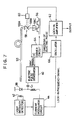
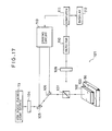
- Fig. 7 exemplarily illustrates the construction of the fourth embodiment applied to nondestructive E - O sampling for example.
- laser light emitted from the LD 38 (pulsed light for sampling) is fed to an optical probe 58 disposed upwardly of an IC 56 to be measured through an optical fiber 55 for example.
- the optical probe 58 comprises a lens 58A, a half mirror 58B and an electrooptic crystal 58C, and is adapted to modulate the pulsed light for sampling by making use of a change in the refractive index of the electrooptic crystal 58C caused by an electric field induced on the surface of the IC 56 by a current flowing through the same.
- the pulsed light modulated by the change in the refractive index is detected by the photodetector 60 and outputted through the lock-in amplifier 62.
- the lock-in amplifier 62 and an IC driver circuit 64 which switches an electric circuit on and off at a lock-in frequency, are controlled by an output from an oscillator 66 for switching an electric pulse on and off and outputs a synchronizing signal to the electric pulse generator 40.
- the present invention were applied to the E - O sampling, the scope of the present invention is not limited thereto, and may clearly be applied also to fluorescence lifetime measurement for measuring laser-excited fluorescence, estimation of response characteristics of a photoelectric detector and an OE IC, etc., and time correlated photon counting method using a photomultiplier, and so on.
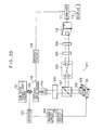
- Fig. 12 is a sectional view, partly including blocks, illustrating the embodiment of the voltage detector device of the type of detecting voltage of an object utilizing a fact that the polarization state of an optical beam is changed owing to voltage at a predetermined portion of the object.
- the voltage detector device 70 comprises an optical probe 72, the same low noise pulsed light source 73 as that illustrated in Figs. 1 through 5, an optical fiber 75 focusing the optical beam emitted from the low noise pulsed light source 73 and quiding the same to the optical probe 72 through a focusing lens 74, an optical fiber 77A for guiding reference light from the optical probe 72 to a photoelectric converter element 77 through a collimator 76, an optical fiber 80A for guiding exit light from the optical probe 72 to a photoelectric converter element 80 through a collimator 79, and a comparator circuit 81 for comparing electric signals subject to the photoelectric conversion from the photoelectric converter elements 77, 80.
- electrooptic materials 72A, 72B each comprising optically uniaxial crystal lithium tantalate (LiTaO3).
- Those electrooptic materials 72A, 72B comprise quite the same material (optically uniaxial crystal) with their length in the directions of the optical probe's axis being made equal to each other but with the optical crystal axes of the electrooptic materials 72A, 72B being directed to be perpendicular to each other.
- a conductive electrode 82 is provided on parts of the outer circumferential portions of the electrooptic materials 72A and 72B, and the tip end of the electrooptic material 72B is coated with a reflecting mirror 83 composed of a metal thin film or a dielectric multi-layer film.
- the optical probe 72 there are further provided a collimator 84, focusing lenses 85, 86, a polarizer 87 for extrating only an optical beam with a predetermined polarized component from an optical beam emanating from the collimator 84, and a beam splitter 89 for dividing the optical beam with the predetermined polarized component from the polarizer 87 to reference light and incident light and for directing the exit light from the electrooptic material 72A to an analyzer 88.
- the reference light and the exit light are guided into the optical fibers 77A, 80A through the focusing lenses 85, 86, respectively.
- the conductive electrode 82 is kept at the earth potential.
- no electric field is therefore existent in the electrooptic material 72A, so that the refractive index of the electrooptic material 72A is not changed owing to the voltage at the predetermined portion of the object.
- the polarization state of the optical beam propagating in the electrooptic material 72A is varied only owing to the phase difference caused by the spontaneous double refraction of the electrooptic material 72A.
- the refractive index is varied by a potential difference between a potential induced on the reflecting mirror 83 owing to voltage on the predetermined portion of the workpiece and the earth potential of the conductive electrode 82. Accordingly, the polarization state of the optical beam propagating in the electrooptic material 72B is varied in accordance with the voltage of the predetermined portion of the object and with the phase difference caused by the spontaneous double refraction of the electrooptic material 72B.
- the optical beam of a predetermined polarized component emanating from the polarizer 87 enters the electrooptic material 72A as incident light through the beam splitter 89.
- the incident 72A is changed in its polarization state owing to the phase difference due to the spontaneous double refraction, and enters the electrooptic material 72A.
- both electrooptic materials 72A and 72B have their lengths in the directions of the optical probe's axis equal to each other, so that the incident light on the electrooptic material 72B is altered in its polarization state oppositely to a case where it enters the electrooptic material 72A, owing to the phase difference due to the spontaneous double refraction of the electrooptic material 72B, and further altered in its polarization state owing to the change in the refractive index based on the potential of the reflecting mirror 83.
- the polarization state of the incident light is therefore changed corresponding to the chance in the refractive index of the electrooptic material 72B based upon the voltage of the predetermined portion of the object, and hence eliminates the influence of the chase difference caused by the spontaneous double refraction.
- the polarization state of the exit light incident on the polarizer 88 is changed from that of the incident light splitted by the beam splitter 89, the change including no influence of the phase difference caused by the spontaneous double refraction of the electrooptic material.
- the tip end of the optical probe 72 is approached to the object, e.g. an integrated circuit (not shown). Owing to this, the refractive index of the tip end of the electrooptic material 72B of the optical probe 72 is changed. More specifically, there is changed a difference between the refractive indexes of ordinary light and extraordinary light in a plane perpendicular to the optical axis in optically uniaxial crystal.
- the optical beam emanating from the low noise pulsed light source 73 enters the collimator 84 of the optical probe 72 through the focusing lens 74 and the optical fiber 75, and is converted as an intensity I optical beam with a predetermined polarized component by the polarizer 87 and is incident on the electrooptic materials 72A, 72B of the optical probe 72 through the beam splitter 89.
- each of the intensities of the reference and incident lights splitted by the beam splitter 89 is of I/2.
- the incident light on the electrooptic material 72B is changed in its polarization state a the tip end of the electrooptic material 72B depending on the change in the refractive index of that tip end and reaches the reflecting mirror 83, on which mirror it is turn reflected back toward the beam splitter 89 as exit light from the electrooptic material 72B.
- the length of the electrooptic material 72B to be 1
- the polarization state of the incident light is changed in proportion to the difference between the refractive indexes of the ordinary light and the extraordinary light and to the length 1.
- the exit light returned back to the beam splitter 89 enters the analyzer 88.
- the intensity of the exit light incident on the analyzer 88 is of I/4 owing to the beam splitter 89.
- the analyzer 88 is constructed so as for only an optical beam of a polarized component perpendicular to the polarization direction of the polarizer 87 to pass therethrough, the intensity I/4 exit light changed in its polarization state and entering the analyzer 88 is modulated in its intensity by the analyzer 88 as ( I / 4 ) sin2 [ ( ⁇ / 2 ) ⁇ V / V 0 ], and is incident on the photoelectric converter element 80.
- V is the voltage on the object
- V0 is half-wavelength voltage.
- the comparater circuit 81 there are compared the intensity I/2 of the reference light converted photoelectrically in the photoelectric converter element 77 and the intensity ( I / 4 ) ⁇ sin2 [ ( ⁇ / 2 ) V / V 0 ] of the exit light converted photoelectrically in the photoelectric converter element 80.
- the intensity of the exit light ( I / 4 ) ⁇ sin2 [ ( ⁇ / 2 ) V / V 0 ] is altered by the change in the refractive index of the tip end 83 of the electrooptic material 72B caused by the voltage change, voltage of an object to be measured, e.g., a predetermined portion of an integrated circuit can be detected on the basis of the alteration of the exit light intensity.
- voltage of a predetermined portion of an object is detected on the basis of the change in the refractive index of the tip end of the electrooptic material 72B which is changed as the tip end of the optical probe 72 approaches the object. Accordingly, there can be detected, without contact with the optical probe 72, voltage of a fine portion of an integrated circuit which is particularly difficult in contact with external means and in which measured voltage is badly affected by contact, if possible, with such external means. Further, with use of the low noise pulsed light source 73 including a laser diode which emits a very short duration optical pulse as the light source, a high speed voltage change can accurately be detected by sampling the high speed voltage change of the object at a ultrashort time interval.
- electrooptic materials such as one used in the optical probe 72 of the voltage detector device 70 illustrated in Fig. 12 after demonstrates inherent double refraction.
- optical uniaxial crystal lithium tantalate (LiTaO3) for example, there is produced a phase difference between ordinary and extraordinary lights of incident light caused by the inherent double refraction proportional to a difference between the refractive indexes n0 and n e of the ordinary and extraordinary lights.
- the chase difference so caused by the inherent double refract ion can be produced even without the application of any voltage to such an optical uniaxial crystal, and alter the polarization state of the incident light.
- a DC component is must be removed from the exit light emanating from the analyzer 88.
- the voltage of the predetermined portion to be measured is one changing at a high speed superimposed on the DC voltage, it is necessary to remove the change in the polarization state which depends on the DC voltage, because only the voltage component changing at a high speed should here be detected.
- phase compensator is provided between the beam splitter 89 and the electrooptic material, which compensator is in turn adjusted to single out only one due to voltage applied to the electrooptic material as the change in the polarization state of the exit light emanating from the electrooptic material.
- This technique however suffers from a problem that even though the phase compensator is adjusted manually to the predetermined value at the initiation of the voltage detection, the adjusted value set upon the initiation of the voltage detection is inadequate and obstructs an accurate result from being detected over the entire period of the voltage detection.
- the electrooptic material 72A which comprises the same material as that of the electrooptic material 72B and has the same length in the direction of the optical probe's axis as that of the same such that the latter electrooptic material 72A is perpendicular in its optical crystal axis to the optical crystal axis of the former.
- the electrooptic material 72A not including therein any electric field, hereby, the changes in the polarization state of the optical beam based on the phase differences by the spontaneous double refractions of the electrooptic materials 72A, 72B can be cancelled each other.
- the polarization state of the exit light incident on the analyzer 88 can be changed with respect to the polarization state of the incident light by the amount dependent on only the voltage applied to the electrooptic material 72B.
- phase changes in the optical beam by the spontaneous double refraction of the electrooptic materials 72A, 72B are changed quite similarly so that the changes in the polarization state of the optical beam based on the phase differences of the same by the spontaneous double refractions can be cancelled at all times.
- phase differences by the spontaneous double refractions of the electrooptic materials are compensated by permitting the first and second electrooptic materials to the disposed such that their optical crystal axes are perpendicular to each other, this may be achieved by other means such as a ⁇ /2 plate 91 for example, instead of the optical probe 90 of the second embodiment of the voltage detector device illustrated in Fig. 13 in which the optical crystal axes of the electrooptic materials 72C and 72B are located perpendicularly to each other.
- the conductive electrode 82 has been provided on the electrooptic material 72C, the outer periphery of the ⁇ /2 plate 91, and part of the outer periphery of the electrooptic material 72B.
- the conductive electrode 82 is kept at ground potential and so no electric field is existent in the electrooptic material 72C.
- FIG. 14 there is illustrated in a sectional view, a portion of the third embodiment of the voltage detector device according to the present invention.
- a voltage detector device 92 of Fig. 4 the same low noise pulsed light source 73 as that described above is used, and there are disposed in an optical probe 93 two electrooptic materials 72a, 72B with their lengths equal to each other in the direction of the optical probe's axis and with their optical crystal axes directed perpendicularly to each other as in the voltage detector device 70 of Fig. 12. Further, a transparent electrode 94 is interposed between the electrooptic materials 72A and 72B and a transparent electrode 95 is provided oppositely to the side of the electrooptic material 72A where the former transparent electrode 94 is provided.
- the transparent electrodes 94, 95 transmit incident light upon and exit light from the electrooptic materials 72A and 72B.
- the transparent electrode 94 is kept at the ground potential and the transparent electrode 95 is subject to variable voltage V B .
- the electrooptic material 72B changes its refractive index owing to a potential difference between the voltage of an object to be measured and the ground potential of the transparent electrode 94
- the electrooptic material 72A changes its refractive index owing to a potential difference between the variable voltage V B exerted on the transparent electrode 95 and th around potential of the transparent electrode 94.
- the transparent electrode 94 is disposed parallely to the reflecting mirror 83 such that electric lines of force from the object through the reflecting mirror 83 is parallely to the central axis of the electrooptic material 72B in the electrooptic material 72B.
- the refractive index change is made uniform everywhere in the electrooptic material 72B.
- the transparent electrode 95 is likewise disposed to be parallel to the transparent electrode 94, so that the refractive index change is made uniform everywhere in the electrooptic material 72A.
- the electrooptic materials 72A and 73B are equal in their lengths to each other and perpendicular in their optical crystal axes as in the voltage detector device 70 of Fig. 1, so that the phase differences by the spontaneous double refractions of those electrooptic materials can be cancelled at all times even though the ambient temperature varies.
- a predetermined refractive index change is produced in the electrooptic material 72A, an operating point shown in Fig. 15 can be shifted from P1 to P2 to eliminate a DC component from the polarization state of the exit light from the electrooptic material 72B. Further, the intensity of the exit light at the operating point P2 is changed as the ambient temperature is changed.
- the operating point P2 is slightly shifted by automatically changing the voltage V B following the temperature change, the variations of the exit light intensity caused by the ambient temperature can be compensated. More specifically, provided the voltage V B is automatically changed following the temperature change to change the refractive index of the electrooptic material 72A, the exit light intensity is prevented from varying as the ambient temperature changes.
- the electrooptic material 72A and 72B can be controlled at all times such that the phase difference of the incident light by the spontaneous double refraction of the electrooptic material can be cancelled at all times, and that the operating point can be set so as for the DC component to be eliminated from the exit light intensity by applying the variable voltage V B to the transparent electrode 95, and further that the exit light intensity from which the DC component has been eliminated can be compensated so as not be varied by the temperature change.
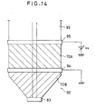
- a voltage detector device 96 there is provided an electrooptic material 97A with its frusto-conical tip end 97B such as optically uniaxial crystal lithium tantalate (LiTaO3) and lithium niobate (LiNbO3), etc., is provided in an optical probe 97 as in the aforementioned voltage detector device, and there is provided a metal thin film reflecting mirror 98 on the tip end 97B of the electrooptic material 97A for reflecting incident light IB having a predetermined polarized component as exit light RB.
- the metal thin film reflecting mirror 98 reflects the incident light IB thereon as described previously and includes voltage at a predetermined portion of an object to be measured.
- a transparent electrode 99 with its surface directed perpendicularly to the central axis A - A of the optical probe 97 is provided above the electrooptic material 97A.
- the transparent electrode 99 is coated thereon with an antireflection film.
- the transparent electrode 99 transmits the incident light IB and reflected light RB without affecting those light and makes uniform a refractive index change in the electrooptic material 97A caused by the voltage at the predetermined portion of the object.
- the low noise pulsed light source 73 and other arrangement are the same as that in the embodiment illustrated in Fig. 12, and hence the illustration and description thereof will be omitted.
- the voltage detector device 96 constructed as described above, once the optical probe 97 is approached to an object 100 to be measured, the voltage at the predetermined portion of the object is induced on the metal thin film reflecting mirror 98. More specifically, there is induced on the metal thin film reflecting mirror 98 a potential caused by voltage of part INAR of the object located just under the reflecting mirror 98 and voltage of part OTAR located outside the part INAR.
- the transparent electrode 99 is kept at around potential for example, there is generated in the electrooptic material 97A an electric line of force ELN1 on the basis of a potential difference between the potential of the metal film reflecting mirror 98 and the around potential of the transparent electrode 99.
- the surface of the transparent electrode 99 is positioned to be perpendicular to the central axis A - A of the optical probe 1 and the transparent electrode 99 is positioned to be parallel to the metal thin film reflecting mirror 98, so that the electric line of force ELN1 generated in the electrooptic material 97A is parallel to the central axis A - A of the electrooptic material 97A.
- the refractive index change of the electrooptic material 97A caused by the electric line of force ELN1 is made uniform over the whole of the electrooptic material 97A, and so the optical beams in the electrooptic material 97A, i.e., the polarized components of the incident light IB and of the reflected light RB are changed accurately corresponding to the voltage of the predetermined portion of the object to permit the voltage of the predetermined portion of the object 100 to be accurately detected.
- the metal thin film reflecting mirror 98 was mounted on the tip end 97B of the electrooptic material 97A, it may be a dielectric multi-layer film.
- an electrooptic material 102 is fixedly mounted in close vicinity of or in contact with an object to be measured such as an IC (integrated circuit) 56, etc.
- the electrooptic material 102 is formed into a columnar or plate shape with its section so cut out as to be enough large compared with that of the electrooptic material contained in the optical probe of the conventional voltage detector device and as to cover a plurality of measurement positions on the IC 56.
- a metal or dielectric multi-layer film reflecting mirror 103 is formed on the bottom of the electrooptic material 102. In the case with the metal reflecting mirror formed, the measurement should be done without making contact with the IC 56 or through an insulator disposed on the surface of the IC 56.
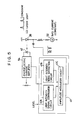
- the voltage detector device 101 includes a low noise pulsed light source 73, a polarizer 104 for extracting a specific polarized component from an optical beam emitted from the low noise pulsed light source 73, two movable mirrors 105, 106 for guiding a predetermined polarized component optical beam extracted through the polarizer 104, a beam splitter 107 for directing to the electrooptic material 102 as incident light the optical beam guided by the movable mirrors 105, 106 and splitting exit light from the electrooptic material 102, an analyzer 109 for extracting a predetermined polarized component from the exit light splitted by the beam splitter 107 and changed in its polarization state, and a detector 110 for receiving exit light from the analyzer 109.
- An electric signal detected by the detector 110 is fed to a computer 111, subject to data processing in the same, stored in a memory (not shown), and displaced on a display 112 upon completion of the voltage detection processing.
- the electrooptic material 102 is cut out so as to cover the plurality of measurement positions of the IC 56 to successively detect voltages at the plurality of measurement positions of the IC 56, as described previously. Thereupon, the incident light is scanned in the directions of X and Y axes as illustrated in Fig. 17 and is satisfactorily focused for its incidence on the electrooptic material 102.
- the movable mirror 105 to provided for scanning of the incident light in the X axis direction, while the movable mirror 106 provided for scanning of the same in the Y axis direction. More specifically, the movable mirrors 105, 106 are driven by a driving circuit 113 controlled by the computer 111 when the computer 111 judges the voltage detection at a certain measurement position on the IC 56 has been completed, to successively scan the optical beam in the directions of the X and Y axes.
- the optical beam from the low noise pulsed light source 73 is extracted in its specific polarized component by the polarizer 104, which component is in turn guided by the movable mirrors 105, 106 and satisfactorily stopped through the beam splitter 107 for incidence on the electrooptic material 102.
- the movable mirrors 105, 106 are assumed to be first set such that the incident light enters the electrooptic material 102 at a location (x1, y1) illustrated in Fig. 18 for example.
- the incident light entering the electrooptic material 102 at that location (x1, y1) is changed in its polarization state is response to that refractive index change, and is reflected on a reflecting mirror 103, allowed to emanate as exit light from the electrooptic material 102, and is received by the detector 110 through the beam splitter 107 and the analyzer 109.
- the detector 110 detects the voltage of the IC 56 at the measurement position of the same located just under the portion of the electrooptic material 102 at the location (x1, y1) of the same, and feeds it to the computer 111.
- the computer 111 executes the predetermined data processing for the voltage at the measurement position of the IC 56 located just under the portion at the detected location (x1, y1), stores it in the memory (not shown), and controls the driving circuit 113 which in turn drives the movable mirror 105 for detecting voltage at a measurement position of the IC 56 located just under a portion of the electrooptic material 102 at a next scanned position of the same.
- the movable mirror 105 is moved in the direction of the axis X so as cause the incident light to enter the electrooptic material 102 at the next scanned position of the same for the same voltage detection processing as in the above description.
- the incident light is set to enter the electrooptic material 102 at the location (x n , y1) of the same, and voltage at a measurement position of the IC 56 located just under a portion of the electrooptic material 102 at a location (x n , y1) of the same has been detected, the computer 111 controls the driving circuit 113 such that the latter drives the movable mirrors 105, 106 for scanning in the direction of the axis X at the next location y2 in the direction of the axis Y.
- the movable mirror 106 is set such that the incident light enters the electrooptic material 102 at the next scanned position y2 in the direction of the axis Y, and the movable mirror 105 is moved from the position x1 to the position x n successively for the same voltage detection processing as described above at the locations from the location (x1, y2) to the location (X n , y2) of the electrooptic material 102.
- the movable mirror 106 is set such that the incident light enters the electrooptic material 102 at the scanned location y n in the direction of the axis Y and the movable mirror 105 is moved successively from the location x1 to the location x n to detect voltages at locations from the location (x1, y m ) to the location (x n , y m ) of the electrooptic material 102 for the completion of the voltage detection at a plurality of the measurement locations of the IC 56.
- a voltage detection result at each measurement position stored in the memory (not shown) of the computer 111 upon the completion of the voltage detection is displayed on the display 112.
- the optical beam stopped onto the electrooptic material 102 is successively scanned in the state of the electrooptic material 102 being fixed and is allowed to be incident upon the electrooptic material 102 to detect the voltages at a plurality of measurement positions of the IC 56.
- an acoustooptic deflector may be incorporated instead of the movable mirrors 105, 106.
- the acoustooptic deflector is driven by a driving circuit controlled by the computer 111 to deflect the optical beam from the polarizer 104 in the directions of the axes X and Y.
- the electrooptic material 102 may instead be scanned by moving the electrooptic material 102 and the object in the directions of the axes X and Y.
- the optical beam from the light source 73 and the polarizer 104 is adapted to directly enter the electrooptic material 102 without being polarized from the beam splitter 107 without intervention of the movable mirrors 105, 106 or the acoustooptic deflector.
- the optical beam incident upon the electrooptic material 102 has satisfactorily stopped.
- the electrooptic material 102 is cut out into a size in its cross section so as to cover a plurality of two-dimensional locations of an object to be measured such as the IC 56 and the like, as in the foregoing embodiment of Fig. 17.
- a metal or dielectric multi-layer reflecting mirror 103 is formed on the bottom of the electrooptic material 102.
- the voltage detector device 114 includes a polarizer 104 for extracting a predetermined polarized component from an optical beam BM emitted from a low noise pulsed light source 73, a micro lens array 115 for dividing an optical beam of the predetermined polarized component extracted by the polarizer to many optical beams BM ij exhibiting together a lattice-shaped pattern, a beam splitter 107 for directing the lattice-shaped pattern many optical beams BM ij divided by the microlens array 111 as incident light toward the electrooptic material 102, and for splitting for voltage detection a lattice-shaped pattern many exit lights SG ij reflected on the reflecting mirror 103 disposed on the bottom of the electrooptic material 102 and emanating from the electrooptic material 102, an analyzer 109 for transmitting therethrough only an optical beam of a predetermined polarized component among the exit lights SG ij from the beam splitter 107, and a detector 116 for receiving the exit light transmitted by
- the microlens array 115 comprises a plurality of first rod lenses 115A all aligned in a specific direction, and a plurality of second rod lenses 115B all aligned in the direction perpendicular to the first rod lenses, both being superimposed, whereby the optical beam is divided into a lattice-shape.
- the detector 11B comprises a two-dimensional photodetector such as a CCD camera, a photodiode array, and a vision camera, etc., and a high speed detector such as a streak camera, etc.
- the electrooptic material 102 is cut out in its section into a size to cover a plurality two-dimensional positions on the IC 56. Accordingly, there are changed refractive indexes of local portions on the electrooptic material 102 corresponding to the two-dimensional positions owing to the voltages at those plurality of the two-dimensional positions of the IC 56.
- those optical beams BM ij of the lattice-shaded pattern having the predetermined polarized component divided by the microlens array 115 propagate along the lattice-shaped part in the electrooptic material 102, those optical beams BM ij are changed in their polarization states owing to the refractive index change at at the lattice-shaped part in the electrooptic material 102 caused by the voltages at the lattice-shaped positions on the IC 56 just under the lattice-shaped part, and allowed to emanate from the electrooptic material 102 as exit lights. These exit lights enter the analyzer 109 via the beam splitter 107.
- the analyzer 109 is adapted to transmit therethrough only the optical beam of the polarized component perpendicular to the polarization direction of the polarizer 104 for example, the exit lights SG ij changed in the polarization states and entering the polarizer 109 are changed in their intensity by the polarizer 109 as being proportional to sin2 [ ( ⁇ / 2 ) ⁇ V i j / V 0 ], and allowed to enter the photodetector 116.
- V ij to the voltage at the two-dimensional lattice position (i, j) on the IC 56
- V0 is a half-wave voltage.
- the intensity of each exit light is changed owing to the refractive index of the local portion on the electrooptic material 102 following the voltage change at each lattice position on the IC 56.
- the detector 116 only the voltages at the two-dimensional lattice positions among overall two-dimensional positions on the object such as the IC 56 can simultaneously be detected.
- a holographic lens may be employed, instead of the microlens array 115 on which such a hologram has been recorded that the optical beam is focused only at a specific two-dimensional portion on the electrooptic material 102.
- a spatial light modulator may be employed instead of the microlens array.
- a similar electrooptic material 102 to those described in the embodiments of Figs. 17 and 19 is disposed in close vicinity to an object to be measured such as the IC 56 or brought into contact with and fixed to the IC 56.
- the electrooptic material 102 is cut down, in its section, into an enough size to cover a plurality of two-dimensional positions on the object.
- a reflecting mirror 103 comprising a metal or dielectric multi-layer film on the bottom of the electrooptic material 102.
- the voltage detector device 117 includes a low noise pulsed light source 73 for emitting a very short pulse duration optical beam, variable delay means 118 for variably delaying the optical beam from the low noise pulsed light source 73, an expanding optical system 119 for expanding and collimating the optical beam delayed by the variable delay means 118 to a two-dimensional expanse, i.e., an expansed and collimated optical beam, a polarizer 104 for extracting a predetermined polarized component from the optical beam collimated by the expanding optical system 119, a beam splitter 107 for directing the collimated light, i.e., optical beam having the predetermined polarized component extracted by the polarizer 104 to the electrooptic material 102 and splitting for the voltage detection exit light reflected on the reflecting mirror 103 formed on the bottom of the electrooptic material 102 and emanating from the electrooptic material 102 and directly the splitted exit light toward a focusing optical system, a phase compensator for adjusting the phase of exit light from the focusing
- the collimated light incident upon the electrooptic material 102 is expanded by the expanding optical system 119 into the two-dimensional expanse, and allowed to enter the electrooptic material 102 uniformly with the predetermined expanse.
- the collimated light incident uniformly upon the electrooptic material 102 is changed in its polarization state owing to the refractive index changes of two-dimensional port ions corresponding to two-dimensional positions on the electrooptic material 102, the change being caused by voltages at a plurality of the two-dimensional positions of the IC 56 as the object, because the electrooptic material 102 has been cut down in its section into a size enough to cover those two-dimensional positions on the object, and is allowed to emanate from the electrooptic material 102 as exit light.
- the exit light emanating from the electrooptic material 102 has identical spreading to that of collimated light, and the changes in the polarization states at various parts of the exit light reflect the voltages at the respective two-dimensional positions on the object.
- the phase compensator 121 is to adjust the phase of the exit light and is to set the polarized component of the exit light extracted by the analyzer 109 to a predetermined angle with respect to that of the collimated light extracted by the polarizer 104, i.e., it is to arrange the polarized component of the exit light extracted by the analyzer 109 in the same direction as or perpendicularly to that of the collimated light extracted by the polarizer 104.
- the detector 116 is a two-dimensional photodetector such as a CCD camera, a photodiode array, and a vidicon camera, etc., and is to detect the intensity of the exit light from the analyzer 109 for simultaneous detection of the voltage at the two-dimensional positions on the object based upon the changes in the refractive indexes of the electrooptic material 102.
- the voltages at the two-dimensional positions on the object must be changed periodically in synchronism with the optical pulse. More specifically, the optical beam from the low noise pulsed light source 73 is halved into two optical beams by the beam splitter 122, one of which is fed to the variable delay means 118 for sampling and the other of which is sent to the detector 123 for photoelectric conversion. An electric signal yielded by the photoelectric conversion reaches the driving circuit 125 via the trigger circuit 124 to actuate the object periodically in synchronism with the optical pulse. Such repeatedly varying voltage is detected by the sampling.
- the sampling is achieved by gradually delaying the optical beam from the low noise pulsed light source 73 by the variable delay means 118, and such operation of the variable delay means 118 is controlled by the computer 111. More specifically, after the detector 116 detects the voltages at the two-dimensional positions on the IC 56 in certain timing, the computer 111 processed those voltages, and stores processed data in the memory (not shown) while controlling the driving circuit 126, which driving circuit 126 in turn drives the variable delay means 115 to delay the optical beam from the low noise pulsed light source 73 and hence slightly shift the sampling timing. Thus, temporal changes in the voltages at the two-dimensional positions on the object can be detected.
- the phase compensator 121 is first adjusted to direct the polarized component of the exit light extracted by the analyzer 109 perpendicularly to that of the collimated light extracted by the polarizer 104.
- the polarization state of the exit light from the electrooptic material 102 is the same as the collimated light incident upon the electrooptic material 102, (when no voltage is applied to the electrooptic material 102), the exit light is prevented from being transmitted by the analyzer 109.
- the chase compensator 121 is set in such a manner, the voltage measurement at the two-dimensional positions on the object is started.
- the electrooptic material 102 is changed in the refractive indexes thereof corresponding to the two-dimensional positions owing to the two-dimensional positions on the object because the electrooptic material 102 has been cut down in its section in to a size enough to cove the two-dimensional positions on the object (IC 56). Accordingly, the collimated light incident uniformly upon the electrooptic state owing to the changes in the refractive indexes of the two-dimensional portions on the electrooptic material 102 corresponding to the two-dimensional positions on the object, and allowed to emanate from the electrooptic material 102 as exit lights.
- exit lights further enters the phase compensator 121 via the beam splitter 107 and the focusing optical system 120, and is adjusted in its chase by the phase compensator 121 and is incident upon the analyzer 109.
- the phase compensator 121 has been adjusted such that the analyzer 109 transmits only the optical beam of the polarized component perpendicular in that the polarizer 104, so that the intensities of the exit lights incident upon the analyzer 109 are allowed to be proportional to sin2 [ ( ⁇ / 2 ) ⁇ V i j / V 0 ] by the analyzer 109 and to enter the analyzer 116.
- V ij is the voltage at the two-dimensional position (i, j) on the object
- V0 is the half-wave voltage.
- the exit lights are changed owing to the chances in the refractive indexes of local portions of the electrooptic material 102 caused by the changes in the voltages at the two-dimensional positions of the object, as described above.
- the detector 116 can therefore detect simultaneously the voltage at the two-dimensional positions on the object such as an integrated circuit on the basis of the refractive index changes.
- the computer 111 stores a detected result in the memory. Further, for detecting the voltage in successive timings, the computer 111 controls the driving circuit 126 to drive the variable delay means 118, whereby the optical beam from the low noise pulsed light source 73 is delayed by a predetermined amount to shift the sampling timing a little at a time for reheated like voltage detection. The temporal changes in the voltages at the two-dimensional positions on the object are thus sampled and measured. The computer 111 stores measured results in the memory, and displays those voltage detection results on the display 112 at the time the sampling measurement within a predetermined time range has been completed, and overall processings are completed.
- Fig. 21 is a block diagram illustrating an eighth embodiment of the voltage detector device in which the voltages at the two-dimensional positions can be displayed, superimposed on the wiring configuration of an object to be measured.
- the same portions as those in Fig. 20 are denoted by the same symbols in Fig. 21, and the description will be omitted.
- an observation light source 131 for emitting pulsed light or DC light to observe the wiring configuration of an object to be measured such as the IC 56 and the like.
- An optical beam emitted from the observation light source 131 has its wavelength different from that of the optical beam emitted from the low noise pulsed light source 73. More specifically, the optical beam from the low noise pulsed light source 73 is reflected on the dielectric multi-layer film mirror 103A formed on the bottom of the electrooptic material 102, whereas the optical beam from the observation light source 131 is transmitted by the dielectric multi-layer film mirror and impinges on the surface of the object.
- the optical beam from the observation light source 131 and the optical beam from the low noise pulsed light source 73 are switched each other by switching means 133 under the control of the computer 111.
- the switching means 133 selects, upon observing the wiring configuration of the object, the optical beam from the observation light source 131 and forces the optical beam to enter the object through the electrooptic material 102, whilst if selects, upon detecting the voltages at the two-dimensional positions on the object, the optical beam from the low noise pulsed light source 73 and forces the same to enter the electrooptic material 102.
- the phase compensator 121 which is adjusted by the computer 111, is adjusted upon observing the wiring configuration of the object, such that the analyzer 109 transmits the exits light of the same polarized component as the polarization direction of the polarizer 104, while it is adjusted, upon detecting the voltages at the two-dimensional positions on the object, such that the analyzer 109 transmits the exit light of the polarized component perpendicular to the polarization direction of the polarizer 104.
- the computer 111 controls, first observing the wiring configuration of an object, the switching means to force the optical beam from the observation light source 131 to enter as collimated light the surface of the object, while it adjusts the chase compensator 121 such that the analyzer 109 transmits the exit light of the same polarized component as the polarization direction of the polarizer 104.
- the optical beam from the observation light source 131 enters as collimated light the electrooptic material 102 through the variable delay means 118, the expanding optical system 119, the polarizer 104, and the beam splitter 107, and is transmitted by the dielectric multi-layer film mirror 103A and permitted to enter the surface of the IC 56 being as the object.
- the collimated light incident upon the surface of the object is partly reflected back depending on the wiring configuration and material duality of the object surface across the dielectric multi-layer film mirror 103A and the electrooptic material 102 and enters the analyzer 109 as exit light via the beam splitter 107, the focusing optical system 120, and the phase compensator 121.
- the phase compensator 121 has been adjusted such at the analyzer 109 transmits the exit light of the same polarized component as the polarization direction of the polarizer 104. Accordingly, the exit light incident upon the analyzer 109 is transmitted by the analyzer 109 intactly and impinges the two-dimensional detector 116 such as a CCD camera.
- the exit light impinging the detector 116 involves visible image information concerning the wiring configuration on the surface of the object.
- the detector 116 subjects it to photoelectric conversion to yield visible image data concerning the wiring configuration.
- the resulting visible image data is fed to be computer 111 and stored in the memory (not shown) of the same.
- the computer 111 subjects the variable delay means 118 to initial setting, and controls the switching means 133 such that the optical beams from the low noise pulsed source 73 enters the electrooptic material 102 as collimated light.
- the computer 111 further adjusts the phase compensator 121 such that the analyzer 109 transmits the exit light of the polarized component perpendicular to the polarization direction of the polarizer 104, to simultaneously detect the voltages at the two-dimensional positions on the object.
- the optical beam from the low noise pulsed light source 73 after entering the electrooptic material 102 as collimated light, is reflected on the dielectric multi-layer film mirror 103A and is changed in its polarization state following the refractive index change of the electrooptic material 102, and further enters as exit light the phase compensator 121 and the analyzer 109.
- the analyzer 109 transmits only the exit light of the predetermined polarized component to permit it to enter the two-dimensional detector 116.
- the detector 116 samples and simultaneously detects the voltages at the two-dimensional positions on the object in timing set by the variable delay means 118.
- a result of the voltage detection in one timing is fed to the computer 111 and stored in the memory. Thereafter, the result of the voltage detection at the two-dimensional positions on the object sampled in the one timing is displayed on the display 112, superimposed on the visible image date concerning the wiring configuration of the object stored previously in the memory.
Landscapes
- Physics & Mathematics (AREA)
- General Physics & Mathematics (AREA)
- Condensed Matter Physics & Semiconductors (AREA)
- Electromagnetism (AREA)
- Optics & Photonics (AREA)
- Measurement Of Current Or Voltage (AREA)
Applications Claiming Priority (2)
| Application Number | Priority Date | Filing Date | Title |
|---|---|---|---|
| JP148943/90 | 1990-06-07 | ||
| JP2148943A JP2777268B2 (ja) | 1989-08-02 | 1990-06-07 | レーザダイオードを用いた低ノイズパルス光源及びこの光源を用いた電圧検出装置 |
Publications (2)
| Publication Number | Publication Date |
|---|---|
| EP0460696A2 true EP0460696A2 (de) | 1991-12-11 |
| EP0460696A3 EP0460696A3 (en) | 1992-09-30 |
Family
ID=15464130
Family Applications (1)
| Application Number | Title | Priority Date | Filing Date |
|---|---|---|---|
| EP19910109352 Withdrawn EP0460696A3 (en) | 1990-06-07 | 1991-06-07 | Low noise pulsed light source utilizing laser diode and voltage detector device utilizing same low noise pulsed light source |
Country Status (2)
| Country | Link |
|---|---|
| US (1) | US5179565A (de) |
| EP (1) | EP0460696A3 (de) |
Cited By (4)
| Publication number | Priority date | Publication date | Assignee | Title |
|---|---|---|---|---|
| EP0552048A3 (en) * | 1992-01-16 | 1994-06-15 | Hamamatsu Photonics Kk | A system for measuring timing relationship between two signals |
| EP0918225A3 (de) * | 1997-11-19 | 2000-08-23 | Ando Electric Co., Ltd. | Elektrooptisches Sampling-Oszilloskop |
| KR100848578B1 (ko) | 2007-03-29 | 2008-07-25 | 한국전기연구원 | 싱글포톤 카운터용 클럭 발생회로 |
| FR2936355A1 (fr) * | 2008-09-23 | 2010-03-26 | Commissariat Energie Atomique | Systeme de controle de derive de gain de photomultiplicateur et procede associe. |
Families Citing this family (27)
| Publication number | Priority date | Publication date | Assignee | Title |
|---|---|---|---|---|
| ATE150573T1 (de) * | 1991-12-30 | 1997-04-15 | Philips Electronics Nv | Optische einrichtung und mit einer solchen optischen einrichtung versehenes gerät zum abtasten einer informationsebene |
| US5402432A (en) * | 1993-06-01 | 1995-03-28 | Quarton, Inc. | Semi-conductor laser device constant power output controller |
| US6239456B1 (en) * | 1998-08-19 | 2001-05-29 | Photobit Corporation | Lock in pinned photodiode photodetector |
| US20040017603A1 (en) * | 2002-07-29 | 2004-01-29 | Paul Jay | Optical amplifier controller |
| US6720734B2 (en) * | 2002-08-08 | 2004-04-13 | Datex-Ohmeda, Inc. | Oximeter with nulled op-amp current feedback |
| DE10358957A1 (de) * | 2003-12-15 | 2005-07-07 | Deutsche Thomson-Brandt Gmbh | Kompatibler optischer Abtaster mit verbessertem Lasermodulator für Aufzeichnungs- oder Wiedergabegeräte optischer Aufzeichnungsträger |
| JP4445836B2 (ja) * | 2004-11-11 | 2010-04-07 | 株式会社アドバンテスト | サンプリング回路及び試験装置 |
| US7646988B2 (en) * | 2006-08-04 | 2010-01-12 | Finisar Corporation | Linear amplifier for use with laser driver signal |
| US7734184B2 (en) * | 2006-08-04 | 2010-06-08 | Finisar Corporation | Optical transceiver module having an active linear optoelectronic device |
| US7873085B2 (en) * | 2007-10-23 | 2011-01-18 | Andrei Babushkin | Method and device for controlling optical output of laser diode |
| US9752932B2 (en) | 2010-03-10 | 2017-09-05 | Drexel University | Tunable electro-optic filter stack |
| US9576694B2 (en) | 2010-09-17 | 2017-02-21 | Drexel University | Applications for alliform carbon |
| JP6159793B2 (ja) | 2013-03-19 | 2017-07-05 | 東芝三菱電機産業システム株式会社 | 表面電位分布計測装置 |
| US9209593B2 (en) * | 2013-12-18 | 2015-12-08 | Tektronix, Inc. | Method of controlling electro-optical probe gain and sensitivity |
| US10187940B2 (en) * | 2015-10-02 | 2019-01-22 | Texas Instruments Incorporated | Transmitter architecture for photoplethysmography systems |
| JP6642154B2 (ja) | 2016-03-17 | 2020-02-05 | 富士通株式会社 | 光送信器および光信号を送信する方法 |
| CN110199204A (zh) * | 2017-03-29 | 2019-09-03 | 深圳市大疆创新科技有限公司 | 具有小形状因子的激光雷达传感器系统 |
| EP3602121A4 (de) | 2017-03-29 | 2021-05-12 | SZ DJI Technology Co., Ltd. | Schaltung zur verarbeitung von lichtdetektions- und entfernungsmessungs (lidar)-signalen |
| CN110383647B (zh) | 2017-03-29 | 2022-10-25 | 深圳市大疆创新科技有限公司 | 中空马达设备及相关系统和方法 |
| CN110573901A (zh) | 2017-04-28 | 2019-12-13 | 深圳市大疆创新科技有限公司 | 激光传感器和视觉传感器的校准 |
| EP3616159A4 (de) | 2017-04-28 | 2020-05-13 | SZ DJI Technology Co., Ltd. | Kalibrierung von lasersensoren |
| EP3615979A4 (de) | 2017-04-28 | 2020-03-25 | SZ DJI Technology Co., Ltd. | Winkelkalibrierung in einem lichtdetektions- und entfernungsmesssystem |
| EP3455645A4 (de) | 2017-07-20 | 2019-04-24 | SZ DJI Technology Co., Ltd. | Systeme und verfahren zur optischen abstandsmessung |
| CN110914703A (zh) | 2017-07-31 | 2020-03-24 | 深圳市大疆创新科技有限公司 | 对点云中基于运动的不准确性的校正 |
| CN111033312A (zh) | 2017-08-31 | 2020-04-17 | 深圳市大疆创新科技有限公司 | 光学距离测量设备的延迟时间校准及相关联的系统和方法 |
| WO2019131410A1 (ja) * | 2017-12-27 | 2019-07-04 | 株式会社Photo electron Soul | 試料検査装置、および、試料検査方法 |
| US11374676B2 (en) | 2018-06-04 | 2022-06-28 | Telefonaktiebolaget Lm Ericsson (Publ) | Optical device and hub node for an optical network |
Family Cites Families (23)
| Publication number | Priority date | Publication date | Assignee | Title |
|---|---|---|---|---|
| NL8005153A (nl) * | 1980-09-15 | 1982-04-01 | Philips Nv | Inrichting voor het moduleren van het uitgangssignaal van een omzetter, bijvoorbeeld een electro-optische omzetter. |
| JPS5783079A (en) * | 1980-11-12 | 1982-05-24 | Sharp Corp | Driving method of semiconductor laser |
| JPS59182637A (ja) * | 1983-03-31 | 1984-10-17 | Matsushita Electric Ind Co Ltd | ビデオ信号光伝送装置 |
| US4618819A (en) * | 1984-03-27 | 1986-10-21 | The University Of Rochester | Measurement of electrical signals with subpicosecond resolution |
| US4689795A (en) * | 1984-04-27 | 1987-08-25 | Mitsubishi Denki Kabushiki Kaisha | Semiconductor laser controller |
| US4698817A (en) * | 1985-02-28 | 1987-10-06 | Northern Telecom Limited | Peak optical power control circuit for laser driver |
| US4733398A (en) * | 1985-09-30 | 1988-03-22 | Kabushiki Kaisha Tohsiba | Apparatus for stabilizing the optical output power of a semiconductor laser |
| US4803384A (en) * | 1985-10-22 | 1989-02-07 | Fujitsu Limited | Pulse amplifier suitable for use in the semiconductor laser driving device |
| US4677632A (en) * | 1985-10-28 | 1987-06-30 | American Telephone And Telegraph Company, At&T Bell Laboratories | Coupled loop controller for a laser transmitter |
| JPS62109382A (ja) * | 1985-11-07 | 1987-05-20 | Fujitsu Ltd | 光出力安定化方式 |
| US4819242A (en) * | 1985-11-20 | 1989-04-04 | Hitachi, Ltd. | Semiconductor laser driver circuit |
| US4799069A (en) * | 1986-04-18 | 1989-01-17 | Minolta Camera Kabushiki Kaisha | Laser recording apparatus |
| KR960015273B1 (ko) * | 1986-05-09 | 1996-11-07 | 아사히 고가구 고교 가부시기가이샤 | 레이저 빔 프린터에서의 반도체 레이저 구동회로 |
| JPS63250966A (ja) * | 1987-04-07 | 1988-10-18 | Asahi Optical Co Ltd | 半導体レ−ザの光出力制御装置 |
| EP0293842B1 (de) * | 1987-05-31 | 1992-08-05 | Hamamatsu Photonics K.K. | Spannungsdetektor |
| US4996475A (en) * | 1987-05-31 | 1991-02-26 | Hamamatsu Photonics Kabushiki Kaisha | Electro-optic voltage detector having a transparent electrode |
| DE3889986T2 (de) * | 1987-07-13 | 1994-09-15 | Hamamatsu Photonics Kk | Anordnung eines Spannungsdetektors. |
| JPH0660912B2 (ja) * | 1987-09-07 | 1994-08-10 | 浜松ホトニクス株式会社 | 電圧検出装置 |
| JPH0758819B2 (ja) * | 1987-09-25 | 1995-06-21 | 株式会社東芝 | 半導体レーザ駆動装置 |
| JPH0666498B2 (ja) * | 1988-05-07 | 1994-08-24 | 浜松ホトニクス株式会社 | 光源駆動装置 |
| JPH0273682A (ja) * | 1988-09-08 | 1990-03-13 | Nippon Digital Equip Kk | レーザダイオード駆動方法及び装置 |
| US5128950A (en) * | 1989-08-02 | 1992-07-07 | Hamamatsu Photonics K.K. | Low noise pulsed light source using laser diode |
| JPH0756257A (ja) * | 1993-08-10 | 1995-03-03 | Konica Corp | ハロゲン化銀写真感光材料 |
-
1991
- 1991-06-05 US US07/710,392 patent/US5179565A/en not_active Expired - Lifetime
- 1991-06-07 EP EP19910109352 patent/EP0460696A3/en not_active Withdrawn
Cited By (6)
| Publication number | Priority date | Publication date | Assignee | Title |
|---|---|---|---|---|
| EP0552048A3 (en) * | 1992-01-16 | 1994-06-15 | Hamamatsu Photonics Kk | A system for measuring timing relationship between two signals |
| US5499190A (en) * | 1992-01-16 | 1996-03-12 | Hamamatsu Photonics K.K. | System for measuring timing relationship between two signals |
| EP0918225A3 (de) * | 1997-11-19 | 2000-08-23 | Ando Electric Co., Ltd. | Elektrooptisches Sampling-Oszilloskop |
| KR100848578B1 (ko) | 2007-03-29 | 2008-07-25 | 한국전기연구원 | 싱글포톤 카운터용 클럭 발생회로 |
| FR2936355A1 (fr) * | 2008-09-23 | 2010-03-26 | Commissariat Energie Atomique | Systeme de controle de derive de gain de photomultiplicateur et procede associe. |
| US8624192B2 (en) | 2008-09-23 | 2014-01-07 | Commissariat A L'energie Atomique Et Aux Energies Alternatives | System for controlling photomultiplier gain drift and associated method |
Also Published As
| Publication number | Publication date |
|---|---|
| US5179565A (en) | 1993-01-12 |
| EP0460696A3 (en) | 1992-09-30 |
Similar Documents
| Publication | Publication Date | Title |
|---|---|---|
| US5179565A (en) | Low noise pulsed light source utilizing laser diode and voltage detector device utilizing same low noise pulsed light source | |
| EP0299432B1 (de) | Anordnung eines Spannungsdetektors | |
| EP0197196A1 (de) | Elektro-elektronenoptisches Oszilloskop zur Zeitauflösung elektrischer Wellenzüge im Picosekundenbereich | |
| EP0411641B1 (de) | Elektro-optischer Abtastapparat mit rauscharmer, gepulster Laserdiode | |
| EP0468632B1 (de) | Schmalbandige Pulslichtquelle und Verwendung derselben in einer Spannungsdetektionsvorrichtung | |
| EP0819924A2 (de) | Gerät und Verfahren für die Messung von Charakteristiken von optischen Pulsen | |
| US4958231A (en) | Electro-optical streak camera | |
| JP4631704B2 (ja) | 半導体デバイスの電界分布測定方法と装置 | |
| US5256968A (en) | Measurement of high-frequency electrical signals by electro-optical effect | |
| US4982151A (en) | Voltage measuring apparatus | |
| US3521958A (en) | Rapid scanning spectrophotometer | |
| JP2777268B2 (ja) | レーザダイオードを用いた低ノイズパルス光源及びこの光源を用いた電圧検出装置 | |
| EP0347054B1 (de) | Vorrichtung zur Korrelation von Lichtintensität | |
| EP0586202B1 (de) | Elektrooptische Sonde | |
| EP0344986B1 (de) | Beobachtungsanordnung für elektrische Signale | |
| JPH0695112B2 (ja) | 電圧検出装置 | |
| EP0506358B1 (de) | Optischer Spannungsdetektor | |
| EP0345011B1 (de) | Elektrische Signalüberwachungsvorrichtung | |
| US5053696A (en) | Electro-electron oscilloscope | |
| JP2675419B2 (ja) | 高感度電圧検出装置 | |
| Ludmirsky et al. | Electro-optical measurements of high potentials in laser produced plasmas with fast time resolution | |
| JP2709170B2 (ja) | 電圧測定装置 | |
| US5625296A (en) | Electro-optic voltage measurement apparatus | |
| US4958124A (en) | Multi-channel voltage detector | |
| JPH08159867A (ja) | 光波形測定装置 |
Legal Events
| Date | Code | Title | Description |
|---|---|---|---|
| PUAI | Public reference made under article 153(3) epc to a published international application that has entered the european phase |
Free format text: ORIGINAL CODE: 0009012 |
|
| AK | Designated contracting states |
Kind code of ref document: A2 Designated state(s): DE FR GB IT |
|
| PUAL | Search report despatched |
Free format text: ORIGINAL CODE: 0009013 |
|
| AK | Designated contracting states |
Kind code of ref document: A3 Designated state(s): DE FR GB IT |
|
| 17P | Request for examination filed |
Effective date: 19921006 |
|
| 17Q | First examination report despatched |
Effective date: 19931209 |
|
| STAA | Information on the status of an ep patent application or granted ep patent |
Free format text: STATUS: THE APPLICATION IS DEEMED TO BE WITHDRAWN |
|
| 18D | Application deemed to be withdrawn |
Effective date: 19950926 |