EP0727877A2 - Synthetisierer mit schneller Frequenzumschaltung - Google Patents
Synthetisierer mit schneller Frequenzumschaltung Download PDFInfo
- Publication number
- EP0727877A2 EP0727877A2 EP96102118A EP96102118A EP0727877A2 EP 0727877 A2 EP0727877 A2 EP 0727877A2 EP 96102118 A EP96102118 A EP 96102118A EP 96102118 A EP96102118 A EP 96102118A EP 0727877 A2 EP0727877 A2 EP 0727877A2
- Authority
- EP
- European Patent Office
- Prior art keywords
- division
- divider
- value
- integer
- frequency
- Prior art date
- Legal status (The legal status is an assumption and is not a legal conclusion. Google has not performed a legal analysis and makes no representation as to the accuracy of the status listed.)
- Granted
Links
Images





Classifications
-
- H—ELECTRICITY
- H03—ELECTRONIC CIRCUITRY
- H03L—AUTOMATIC CONTROL, STARTING, SYNCHRONISATION OR STABILISATION OF GENERATORS OF ELECTRONIC OSCILLATIONS OR PULSES
- H03L7/00—Automatic control of frequency or phase; Synchronisation
-
- H—ELECTRICITY
- H03—ELECTRONIC CIRCUITRY
- H03L—AUTOMATIC CONTROL, STARTING, SYNCHRONISATION OR STABILISATION OF GENERATORS OF ELECTRONIC OSCILLATIONS OR PULSES
- H03L7/00—Automatic control of frequency or phase; Synchronisation
- H03L7/06—Automatic control of frequency or phase; Synchronisation using a reference signal applied to a frequency- or phase-locked loop
- H03L7/08—Details of the phase-locked loop
- H03L7/10—Details of the phase-locked loop for assuring initial synchronisation or for broadening the capture range
- H03L7/107—Details of the phase-locked loop for assuring initial synchronisation or for broadening the capture range using a variable transfer function for the loop, e.g. low pass filter having a variable bandwidth
-
- H—ELECTRICITY
- H03—ELECTRONIC CIRCUITRY
- H03L—AUTOMATIC CONTROL, STARTING, SYNCHRONISATION OR STABILISATION OF GENERATORS OF ELECTRONIC OSCILLATIONS OR PULSES
- H03L7/00—Automatic control of frequency or phase; Synchronisation
- H03L7/06—Automatic control of frequency or phase; Synchronisation using a reference signal applied to a frequency- or phase-locked loop
- H03L7/08—Details of the phase-locked loop
- H03L7/10—Details of the phase-locked loop for assuring initial synchronisation or for broadening the capture range
- H03L7/107—Details of the phase-locked loop for assuring initial synchronisation or for broadening the capture range using a variable transfer function for the loop, e.g. low pass filter having a variable bandwidth
- H03L7/1075—Details of the phase-locked loop for assuring initial synchronisation or for broadening the capture range using a variable transfer function for the loop, e.g. low pass filter having a variable bandwidth by changing characteristics of the loop filter, e.g. changing the gain, changing the bandwidth
-
- H—ELECTRICITY
- H03—ELECTRONIC CIRCUITRY
- H03L—AUTOMATIC CONTROL, STARTING, SYNCHRONISATION OR STABILISATION OF GENERATORS OF ELECTRONIC OSCILLATIONS OR PULSES
- H03L7/00—Automatic control of frequency or phase; Synchronisation
- H03L7/06—Automatic control of frequency or phase; Synchronisation using a reference signal applied to a frequency- or phase-locked loop
- H03L7/16—Indirect frequency synthesis, i.e. generating a desired one of a number of predetermined frequencies using a frequency- or phase-locked loop
- H03L7/18—Indirect frequency synthesis, i.e. generating a desired one of a number of predetermined frequencies using a frequency- or phase-locked loop using a frequency divider or counter in the loop
- H03L7/197—Indirect frequency synthesis, i.e. generating a desired one of a number of predetermined frequencies using a frequency- or phase-locked loop using a frequency divider or counter in the loop a time difference being used for locking the loop, the counter counting between numbers which are variable in time or the frequency divider dividing by a factor variable in time, e.g. for obtaining fractional frequency division
- H03L7/1972—Indirect frequency synthesis, i.e. generating a desired one of a number of predetermined frequencies using a frequency- or phase-locked loop using a frequency divider or counter in the loop a time difference being used for locking the loop, the counter counting between numbers which are variable in time or the frequency divider dividing by a factor variable in time, e.g. for obtaining fractional frequency division for reducing the locking time interval
-
- H—ELECTRICITY
- H03—ELECTRONIC CIRCUITRY
- H03L—AUTOMATIC CONTROL, STARTING, SYNCHRONISATION OR STABILISATION OF GENERATORS OF ELECTRONIC OSCILLATIONS OR PULSES
- H03L7/00—Automatic control of frequency or phase; Synchronisation
- H03L7/06—Automatic control of frequency or phase; Synchronisation using a reference signal applied to a frequency- or phase-locked loop
- H03L7/16—Indirect frequency synthesis, i.e. generating a desired one of a number of predetermined frequencies using a frequency- or phase-locked loop
- H03L7/18—Indirect frequency synthesis, i.e. generating a desired one of a number of predetermined frequencies using a frequency- or phase-locked loop using a frequency divider or counter in the loop
- H03L7/197—Indirect frequency synthesis, i.e. generating a desired one of a number of predetermined frequencies using a frequency- or phase-locked loop using a frequency divider or counter in the loop a time difference being used for locking the loop, the counter counting between numbers which are variable in time or the frequency divider dividing by a factor variable in time, e.g. for obtaining fractional frequency division
- H03L7/1974—Indirect frequency synthesis, i.e. generating a desired one of a number of predetermined frequencies using a frequency- or phase-locked loop using a frequency divider or counter in the loop a time difference being used for locking the loop, the counter counting between numbers which are variable in time or the frequency divider dividing by a factor variable in time, e.g. for obtaining fractional frequency division for fractional frequency division
- H03L7/1976—Indirect frequency synthesis, i.e. generating a desired one of a number of predetermined frequencies using a frequency- or phase-locked loop using a frequency divider or counter in the loop a time difference being used for locking the loop, the counter counting between numbers which are variable in time or the frequency divider dividing by a factor variable in time, e.g. for obtaining fractional frequency division for fractional frequency division using a phase accumulator for controlling the counter or frequency divider
-
- H—ELECTRICITY
- H03—ELECTRONIC CIRCUITRY
- H03L—AUTOMATIC CONTROL, STARTING, SYNCHRONISATION OR STABILISATION OF GENERATORS OF ELECTRONIC OSCILLATIONS OR PULSES
- H03L7/00—Automatic control of frequency or phase; Synchronisation
- H03L7/06—Automatic control of frequency or phase; Synchronisation using a reference signal applied to a frequency- or phase-locked loop
- H03L7/08—Details of the phase-locked loop
- H03L7/085—Details of the phase-locked loop concerning mainly the frequency- or phase-detection arrangement including the filtering or amplification of its output signal
- H03L7/089—Details of the phase-locked loop concerning mainly the frequency- or phase-detection arrangement including the filtering or amplification of its output signal the phase or frequency detector generating up-down pulses
- H03L7/0891—Details of the phase-locked loop concerning mainly the frequency- or phase-detection arrangement including the filtering or amplification of its output signal the phase or frequency detector generating up-down pulses the up-down pulses controlling source and sink current generators, e.g. a charge pump
- H03L7/0895—Details of the current generators
- H03L7/0898—Details of the current generators the source or sink current values being variable
Definitions
- the present invention relates to a frequency synthesizer which operates by heightening the frequency of reference signal higher than the output frequency interval that can be set, in order to change over the output signal frequency at high speed.
- the fractional-N synthesizer is a method of changing the division value of the RF divider in time, realizing the division value at a precision of below the decimal point as the average value, and heightening the reference frequency higher than the output signal frequency interval, and since the reference frequency is high, the output signal frequency can be changed over at high speed.
- Fig. 11 shows a structural diagram of frequency synthesizer of the conventional fractional-N system.
- reference numeral 901 is a VCO (voltage controlled oscillator)
- 902 is an RF divider
- 903 is a reference divider
- 904 is a phase/frequency comparator
- 905 is a loop filter
- 906 is an RF divider controller
- 907 is a reference divider controller.
- the RF divider 902 divides and outputs the output signal frequency of the VCO 901 according to the value set in the RF divider controller.
- the reference divider 903 divides and outputs the reference signal according to the value set in the reference divider controller 907.
- the phase/frequency comparator 904 compares the phase between the output signal of the RF divider 902 and the output signal of the reference divider 903, and outputs a phase error.
- the output of the phase/frequency comparator 904 is put into the VCO 901 through the loop filter 905, and the output signal frequency is controlled so that the output signal of the VCO 901 may be phase-locked in the output signal of the reference divider 903.
- the output of the VCO 901 is delivered outside as output signal, and is also fed into the RF divider 902.
- the RF divider controller 906 outputs an integer value which changes periodically so that the average of the output values to the RF divider 902 may be a fractional value, and the reference divider controller 907 outputs a specific integer value to the reference divider 903.
- the output signal frequency of the VCO 901 is the product of the phase comparison frequency of the phase/frequency comparator 904 multiplied by the average of the division value of the RF divider 902.
- the invention presents a fast frequency switching synthesizer comprising a reference divider for dividing a reference source signal, a VCO (voltage controlled oscillator), an RF divider for dividing the output signal of the VCO, a phase/frequency comparator for comparing the phases of the output signal of the RF divider and the output signal of the reference divider, a loop filter for receiving a detected phase error and issuing a control voltage of the VCO, and a division value controller for changing the division value of the RF divider to obtain a fractional value as the average of the value obtained by changing periodically the value of the integer when changing the output signal frequency of the VCO, for changing the division value of the RF divider to obtain an integer value not changing after change of the output signal frequency is substantially completed, and determining the division value of the reference divider as the division value corresponding to the integer value.
- VCO voltage controlled oscillator
- the output frequency of the VCO can be switched fast by heightening the reference frequency which is the output of the reference and widening the loop bandwidth. After the output frequency is changed, it operates as an ordinary frequency synthesizer not changing in the division value, so that the spurious signal can be suppressed.
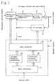
- Fig. 1 is a structural diagram of a frequency synthesizer according to the invention.
- reference numeral 1 is a VCO (voltage controlled oscillator)
- 2 is an RF divider
- 3 is a reference divider
- 4 is a phase/frequency comparator
- 5 is a loop filter
- 6 is a division value control circuit.
- the RF divider 2 divides and outputs the output signal frequency of the VCO 1 according to the value set in the division value control circuit 6.
- the reference divider 3 divides and outputs the reference signal according to the value set in the division value control circuit 6.
- the phase/frequency comparator 4 compares the phases of the output signal of the RF divider 2 and output signal of the reference divider 3, and outputs a phase error.
- the output of the phase/frequency comparator 4 is fed into the VCO 1 through the loop filter 5, and controls the output signal frequency so that the output signal of the VCO 1 may be phase-locked in the output signal of the reference divider 3.
- the output of the VCO 1 is issued outside as output signal, and is also fed into the RF divider 2.
- the division value control circuit 6 comprises a data converter 7, a fractional division controller 8, an integer division controller 9, and a data selector 10.
- the serial data entering from outside is fed into the fractional division controller 8 and integer division controller 9 through the data converter 7, and either output of the fractional division controller 8 or the integer division controller 9 is selected by the data selector 10 depending on the select signal, and the division value of the RF divider 2 and reference divider 3 is controlled.
- a fractional division means that the division value (which means a value utilized for frequency dividing operation) of the frequency divider for the output signal frequency of the voltage controlled oscillator is variable, and a integer division means that the division value of the frequency divider for the output signal frequency of the voltage controlled oscillator is fixed.
- FIG. 2 A detailed structure of the division value control circuit 6 is shown in Fig. 2.
- reference numeral 101 is an accumulator
- 102 is an adder
- 103 is a register
- 104 is an integer part adder
- 105 is a synchronizer
- 106 is a serial-parallel converter
- 107 is a data register for RF divider
- 108 is a data register for reference divider
- 109 is a switch.
- the serial-parallel converter 106 converts the serial data entering from outside into parallel data, and stores in the data register for RF divider 107 and data register for reference divider 108.
- the integer division controller 9 outputs the values of the data register for RF divider 107 and data register for reference divider 108 directly into the data selector 10.
- the fractional division controller 8 outputs the upper bits excluding lower bits of the data register for reference divider 108 into the data selector 10. Of the data entering from the data register for RF divider 107 into the fractional division controller 8, lower n bits enter the accumulator 101 and upper bits enter the integer part adder 104.
- the accumulator 101 is composed of the adder 102 and register 103.
- the adder 102 adds the input n-bit data K and the output of the register 103, and outputs the result to the register 103.
- the register 103 updates the output at every clock.
- the integer part adder 104 outputs M when the input data M has no carry signal, and (M+1) if having carry signal. Therefore, in the period of L locks, the division value is (M+1) in K times, and M in (L-K) times, and the average in this period is ( M+K/L ).
- the division value can be made in 1/L step.
- M occurs 7 times in the period of 8 clocks, and (M+1) once, and the average is 1/8.
- the synchronizer 105 synchronizes the changing timing of the select signal entering from outside with the clock.
- the data selector 10 selects either one of the outputs of the fractional division controller 8 and integer division controller 9 depending on the output of the synchronizer 105.
- the output of the synchronizer 105 controls the switch 109 when the output of the integer division controller 9 is selected, and stops the clock of the accumulator 101.
- the division values of the reference divider 3 and RF divider 2 delivered by the integer division controller 9 are L times of the division value of the reference divider 3 and the average division value of the RF divider 2 delivered by the fractional division controller 8.
- the output signal frequency of the VCO 1 is expressed by the product of the phase comparison frequency of the phase/frequency comparator 4 and the division value of the RF divider 2, and therefore the center frequency of the output signal of the VCO 1 may be equal whether the output of the fractional division controller 8 or the output of the integer division controller 9 is used.
- the data selector 10 selects the output of the fractional division controller 8 by the select signal, and performs fractional division operation. At the timing when the output signal frequency is nearly changed over, it is switched to the output of the integer division controller 9, and integer division operation is conducted.
- the phase comparison frequency of the phase/frequency comparator 4 is L times, so that the frequency can be changed over at high speed. Switching is followed by integer division operation with constant division value, so that the spurious signal is small.
- the fractional division operation and integer division operation can be changed over. Since the fractional division operation and integer division operation are synchronized with the clock, error does not occur in switching operation. When changing over the frequency, first the fractional division operation of high phase comparison frequency is done, which is followed by the integer division operation, and hence the frequency can be switched fast and the characteristic of low spurious signal in output signal is realized. Besides, in the integer division operation, since the clock of the fractional division controller is stopped, there is no current consumption.
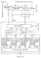
- FIG. 4 is a structural diagram of the frequency synthesizer of the second embodiment of the invention.
- the basic constitution in Fig. 4 is same as in Fig. 1, except that only the constitution of the data converter is different, and same parts as in Fig. 1 are identified with same reference numerals and duplicate explanations are omitted.
- reference numeral 201 is a serial-parallel converter
- 202 is a data register for RF divider in fractional division operation
- 203 is a data register for reference divider in fractional division operation
- 204 is a data register for RF divider in integer division operation
- 205 is a data register for reference divider in integer division operation.
- the serial data entering from outside is converted into parallel data in the serial-parallel converter 201.
- the data contains address information, and depending on this value, it is stored in any one of the data register for RF divider in fractional division operation 202, data register for reference divider in fractional division operation 203, data register for RF divider in integer division operation 204, and data register for reference divider in integer division operation 205.
- the outputs of the data register for RF divider in fractional division operation 202 and data register for reference divider in fractional division operation 203 are fed into the fractional division controller 8, and the outputs of the data register for RF divider in integer division operation 204 and data register for reference divider in integer division operation 205 are fed into the integer division controller 9.
- the fractional division controller 9 periodically changes the division value of the integer to the RF divider 2, and outputs the division value of fractional value as the average, and performs fractional division operation.
- the integer division controller 9 directly outputs the division value of the input integer value, and performs integer division operation. Either output of the fractional division controller 8 or integer division controller 9 is selected by the data selector 10 depending on the select signal, and the division values of the RF divider 2 and reference divider 3 are controlled.
- the value of n varies by changing the input data.
- the output signal frequency of the VCO 1 is expressed by the product of the phase comparison frequency of the phase/frequency comparator 4 and division value of the RF divider 2, and therefore the center frequency of the output signal of the VCO 1 is equal whether the output of the fractional division controller 8 or the integer division controller 9 is used.
- the data selector 10 selects the output of the fractional division controller 8 by the select signal, and performs fractional division operation. Then, at the timing when the output signal frequency is nearly changed over, it is changed over to the output of the integer division controller 9 to perform integer division operation.
- the phase comparison frequency of the phase/frequency comparator 4 is L times, so that the frequency can be changed over at high speed. Switching is followed by integer division operation with constant division value, so that the spurious signal is small.
- the fractional division operation of high phase comparison frequency is done, which is followed by the integer division operation, and hence the frequency can be switched fast and the characteristic of low spurious signal in output signal is realized. Since the data can be set independently in the fractional division operation and integer division operation, the ratio of the phase comparison frequency of fractional division operation and integer division operation can be set freely in the cumulative unit of 2.
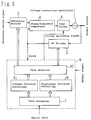
- Fig. 5 is a structural diagram of the frequency synthesizer of the second embodiment of the invention.
- the basic constitution in Fig. 5 is same as in Fig. 1, except that only the constitution of the phase/frequency comparator 4 and loop filter 5 is different, and same parts as in Fig. 1 are identified with same reference numerals and duplicate explanations are omitted.
- the constitution of the division value control circuit 6 in Fig. 5 is same as shown in Fig. 2.
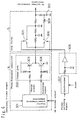
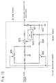
- Fig. 6 is a structural diagram of the phase/frequency comparator and loop filter of the embodiment.
- reference numeral 301 is a digital phase/frequency comparator
- 302 is a charge pump.
- the phase/frequency comparator 4 comprises the digital phase/frequency comparator 301 and charge pump 302.
- the digital phase/frequency comparator 301 detects a phase error of the reference divider output and RF divider output, and sends a pulse charge signal or discharge signal into the charge pump 302.
- the charge pump 302 is composed of PNP transistor 302 and NPN transistor 303 having their collectors connected with each other. The output signals from the collectors of the PNP transistor 302 and NPN transistor 303 are fed into the loop filter 5.
- the loop filter 5 is a passive filter composed of resistance and capacitor, and comprises a switch 305 for connecting the input end and a point in the inside, and a switch 306 for connecting the input end and a capacitor 310 largest in the capacitance of the inside through a resistance 309.
- the loop filter 5 is wide in the pass bandwidth when the switch 305 and switch 306 are ON, and narrow in the pass bandwidth when the switch 305 and the switch 306 are OFF.
- the filter switching signal controls the switch 305 and switch 306 through a synchronizer 307 and a delay circuit 308.
- the synchronizer 307 synchronizes the change of select signal with the clock, and the delay circuit 308 delays the signal by the loop filter composed of resistance and capacitor and the amplifier.
- the filter switching signal and select signal are changed at the timing shown in Fig. 7.
- the data selector 10 selects the output of the fractional division controller 8 by the select signal, and performs fractional division operation.
- the loop filter 5 is extended in the pass bandwidth as the switch 305 and switch 306 are turned on by the filter switching signal.
- the switch 305 and switch 306 are turned off by the filter switching signal, and the pass bandwidth of the loop filter 5 is narrowed.
- the data selector 10 selects the output of the integer division controller 9 by the select signal, and performs integer division operation.
- Fig. 8 is a detailed diagram of the timing of turning off the switch 305 and switch 306 by the filter switching signal. While the output of the charge pump is in high impedance state by the synchronizer 307 and delay circuit 308, the filter switching signal turns off the switch 305 and switch 306.
- the charge signal is fed into the base of the PNP transistor 303 through the resistance 403 selected by the switch 401.
- the discharge signal is fed into the base of the NPN transistor 304 through the resistance 405 selected by the switch 402.
- the switch 401 selects the resistance 404, and the switch 402 selects the resistance 406.
- the resistance value of the resistance 403 is smaller than that of the resistance 404, and the resistance value of the resistance 405 is smaller than that of the resistance 406.
- the switch 401 and switch 402 are controlled by the select signal through the synchronizer 407 and delay circuit 8.
- the synchronizer 407 synchronizes the change of select signal with the clock, and the delay circuit 408 delays the signal by the loop filter composed of resistance and capacitor and the amplifier.
- the delay circuit 408 delays the signal by the loop filter composed of resistance and capacitor and the amplifier.
- Fig. 10 is a diagram showing other structural example of the loop filter 5 in Fig. 6.
- This loop filter is composed by adding a capacitor 501, an AC inverter 502, and a voltage adder 503 to the loop filter in Fig. 6.
- the AC inverter 502 detects the voltage fluctuation applied to the capacitor 310 through the capacitor 501, and adds an inverted signal to the loop filter 5 through the voltage adder 503.
- the AC inverter 502 stops its operation when the select signal specifies integer division operation.
- the voltage of parts in the loop filter also fluctuates largely in period depending on the change of division value of the RF divider 2. This fluctuation is canceled by generating and adding an inverted signal of periodic voltage fluctuations by the AC inverter 502. Accordingly, the fluctuations are smaller when changed over to the integer division operation, and the subsequent convergence is quick.
- phase/frequency comparator 4 and loop filter 5 shown in this embodiment may be also applied in the frequency synthesizer shown in Fig. 4.
- the division value of the reference divider 3 is set small and the division value of the RF divider 2 is also set small to perform fractional division operation for changing periodically, and it is followed by the integer division operation in which the division values of the reference divider 3 and RF divider 2 are large and constant integer values, and therefore the output signal frequency can be changed over at high speed because the phase comparison frequency is high.
- the fluctuations of control voltage of the VCO 1 may be extremely small, so that the spurious signal of output signal may be very small.
Landscapes
- Stabilization Of Oscillater, Synchronisation, Frequency Synthesizers (AREA)
Applications Claiming Priority (3)
| Application Number | Priority Date | Filing Date | Title |
|---|---|---|---|
| JP2502695 | 1995-02-14 | ||
| JP02502695A JP3327028B2 (ja) | 1995-02-14 | 1995-02-14 | 周波数シンセサイザ |
| JP25026/95 | 1995-02-14 |
Publications (3)
| Publication Number | Publication Date |
|---|---|
| EP0727877A2 true EP0727877A2 (de) | 1996-08-21 |
| EP0727877A3 EP0727877A3 (de) | 1997-02-12 |
| EP0727877B1 EP0727877B1 (de) | 2002-11-20 |
Family
ID=12154411
Family Applications (1)
| Application Number | Title | Priority Date | Filing Date |
|---|---|---|---|
| EP96102118A Expired - Lifetime EP0727877B1 (de) | 1995-02-14 | 1996-02-13 | Synthetisierer mit schneller Frequenzumschaltung |
Country Status (5)
| Country | Link |
|---|---|
| US (1) | US5694089A (de) |
| EP (1) | EP0727877B1 (de) |
| JP (1) | JP3327028B2 (de) |
| KR (1) | KR100361855B1 (de) |
| DE (1) | DE69624855T2 (de) |
Cited By (10)
| Publication number | Priority date | Publication date | Assignee | Title |
|---|---|---|---|---|
| FR2756685A1 (fr) * | 1996-12-03 | 1998-06-05 | Philips Electronics Nv | Synthetiseur de frequence programmable a faible sensibilite au bruit de phase |
| WO1999013594A1 (en) * | 1997-09-11 | 1999-03-18 | Telefonaktiebolaget Lm Ericsson | Apparatus and method for radio communication |
| WO2000041307A1 (en) * | 1998-12-16 | 2000-07-13 | International Business Machines Corporation | Combined read and write vco for dasd prml channels |
| EP1030453A1 (de) * | 1999-01-20 | 2000-08-23 | Sony International (Europe) GmbH | Methode zur Verringerung der Einschwingzeit eines PLL-Frequenzsynthetisierers mit progammierbaren Frequenzteiler |
| EP0874463A3 (de) * | 1997-04-25 | 2000-12-06 | Matsushita Electric Industrial Co., Ltd. | Mehrband-Frequenzsynthetisierer |
| EP1067693A1 (de) * | 1999-06-30 | 2001-01-10 | Infineon Technologies AG | PLL-Synthesizer |
| WO2002001721A1 (fr) * | 2000-06-30 | 2002-01-03 | Alcatel | Procede et dispositif de synthese de frequence au moyen d'une boucle a phase asservie |
| GB2373936A (en) * | 2000-12-08 | 2002-10-02 | Agilent Technologies Inc | Frequency Synthesizer |
| WO2004034586A3 (en) * | 2002-10-08 | 2004-07-01 | Ma Com Inc | Methods and apparatus for signal modification in a fractional-n phase locked loop system |
| US7203262B2 (en) | 2003-05-13 | 2007-04-10 | M/A-Com, Inc. | Methods and apparatus for signal modification in a fractional-N phase locked loop system |
Families Citing this family (21)
| Publication number | Priority date | Publication date | Assignee | Title |
|---|---|---|---|---|
| JP3679503B2 (ja) * | 1996-06-11 | 2005-08-03 | 松下電器産業株式会社 | 周波数シンセサイザ |
| US5859549A (en) * | 1997-06-13 | 1999-01-12 | Tektronix, Inc. | Digital audio frame and block synchonization |
| DE19946200A1 (de) | 1999-09-27 | 2001-05-03 | Infineon Technologies Ag | Phasenregelkreis |
| US6366174B1 (en) | 2000-02-21 | 2002-04-02 | Lexmark International, Inc. | Method and apparatus for providing a clock generation circuit for digitally controlled frequency or spread spectrum clocking |
| JP2001298363A (ja) * | 2000-04-17 | 2001-10-26 | Matsushita Electric Ind Co Ltd | 周波数シンセサイザ装置とそれを用いた移動無線機 |
| US6763474B1 (en) | 2000-08-03 | 2004-07-13 | International Business Machines Corporation | System for synchronizing nodes in a heterogeneous computer system by using multistage frequency synthesizer to dynamically adjust clock frequency of the nodes |
| US6522207B1 (en) | 2000-08-03 | 2003-02-18 | International Business Machines Corporation | Apparatus and method for dynamic frequency adjustment in a frequency synthesizer |
| US6566921B1 (en) | 2000-08-03 | 2003-05-20 | International Business Machines Corporation | Apparatus and method for high resolution frequency adjustment in a multistage frequency synthesizer |
| KR100725935B1 (ko) * | 2001-03-23 | 2007-06-11 | 삼성전자주식회사 | 프랙셔널-앤 주파수 합성기용 위상 고정 루프 회로 |
| US6658043B2 (en) | 2001-10-26 | 2003-12-02 | Lexmark International, Inc. | Method and apparatus for providing multiple spread spectrum clock generator circuits with overlapping output frequencies |
| US6946884B2 (en) * | 2002-04-25 | 2005-09-20 | Agere Systems Inc. | Fractional-N baseband frequency synthesizer in bluetooth applications |
| US7356111B1 (en) * | 2003-01-14 | 2008-04-08 | Advanced Micro Devices, Inc. | Apparatus and method for fractional frequency division using multi-phase output VCO |
| US6928127B2 (en) * | 2003-03-11 | 2005-08-09 | Atheros Communications, Inc. | Frequency synthesizer with prescaler |
| US7282967B2 (en) * | 2003-10-30 | 2007-10-16 | Avago Technologies General Ip ( Singapore) Pte. Ltd. | Fixed frequency clock output having a variable high frequency input clock and an unrelated fixed frequency reference signal |
| US7231012B2 (en) * | 2004-11-30 | 2007-06-12 | Stmicroelectronics Pvt. Ltd. | Programmable frequency divider |
| US8014477B1 (en) | 2006-03-08 | 2011-09-06 | Marvell International Ltd. | Receiver employing selectable A/D sample clock frequency |
| US8044723B2 (en) * | 2007-09-14 | 2011-10-25 | Qualcomm Incorporated | Oscillator signal generation with spur mitigation in a wireless communication device |
| KR100972818B1 (ko) * | 2008-01-16 | 2010-07-28 | 국민대학교산학협력단 | 디엘엘 기반의 분수체배 주파수 합성 장치 및 방법 |
| US9287886B2 (en) | 2008-02-29 | 2016-03-15 | Qualcomm Incorporated | Dynamic reference frequency for fractional-N Phase-Locked Loop |
| US7701298B2 (en) * | 2008-08-19 | 2010-04-20 | Megawin Technology Co., Ltd. | Frequency locking structure applied to phase-locked loops |
| US8145171B2 (en) * | 2008-10-08 | 2012-03-27 | Qualcomm Incorporated | Clock clean-up phase-locked loop (PLL) |
Family Cites Families (10)
| Publication number | Priority date | Publication date | Assignee | Title |
|---|---|---|---|---|
| JPS61131914A (ja) * | 1984-11-30 | 1986-06-19 | Yokogawa Hewlett Packard Ltd | 周播数合成装置 |
| US5018170A (en) * | 1989-11-21 | 1991-05-21 | Unisys Corporation | Variable data rate clock synthesizer |
| DE3939709A1 (de) * | 1989-12-01 | 1991-06-06 | Bosch Gmbh Robert | Verfahren zur abstimmung eines funksende- und/oder -empfangsgeraetes |
| FR2656480B1 (fr) * | 1989-12-22 | 1994-04-15 | Thomson Csf | Synthetiseur hyperfrequence a division fractionnaire. |
| US5038117A (en) * | 1990-01-23 | 1991-08-06 | Hewlett-Packard Company | Multiple-modulator fractional-N divider |
| US5021754A (en) * | 1990-07-16 | 1991-06-04 | Motorola, Inc. | Fractional-N synthesizer having modulation spur compensation |
| FR2666184A1 (fr) * | 1990-08-24 | 1992-02-28 | Alcatel Radiotelephone | Horloge a division de frequence fractionnaire et asservissement de cette horloge. |
| US5256981A (en) * | 1992-02-27 | 1993-10-26 | Hughes Aircraft Company | Digital error corrected fractional-N synthesizer and method |
| US5420545A (en) | 1993-03-10 | 1995-05-30 | National Semiconductor Corporation | Phase lock loop with selectable frequency switching time |
| JP3033654B2 (ja) * | 1993-08-23 | 2000-04-17 | 日本電気株式会社 | Pll周波数シンセサイザ |
-
1995
- 1995-02-14 JP JP02502695A patent/JP3327028B2/ja not_active Expired - Lifetime
-
1996
- 1996-02-13 US US08/600,683 patent/US5694089A/en not_active Expired - Lifetime
- 1996-02-13 EP EP96102118A patent/EP0727877B1/de not_active Expired - Lifetime
- 1996-02-13 KR KR1019960003432A patent/KR100361855B1/ko not_active Expired - Fee Related
- 1996-02-13 DE DE69624855T patent/DE69624855T2/de not_active Expired - Fee Related
Cited By (20)
| Publication number | Priority date | Publication date | Assignee | Title |
|---|---|---|---|---|
| EP0847143A1 (de) * | 1996-12-03 | 1998-06-10 | Koninklijke Philips Electronics N.V. | Programmierbarer Frequenzsynthetisierer mit geringer Empfindlichkeit gegen Phasenrauschen |
| US5880642A (en) * | 1996-12-03 | 1999-03-09 | U.S. Philips Corporation | Programmable frequency synthesizer having a low sensitivity to phase noise |
| FR2756685A1 (fr) * | 1996-12-03 | 1998-06-05 | Philips Electronics Nv | Synthetiseur de frequence programmable a faible sensibilite au bruit de phase |
| EP0874463A3 (de) * | 1997-04-25 | 2000-12-06 | Matsushita Electric Industrial Co., Ltd. | Mehrband-Frequenzsynthetisierer |
| GB2344949B (en) * | 1997-09-11 | 2001-09-26 | Ericsson Telefon Ab L M | Apparatus and method for radio communication |
| WO1999013594A1 (en) * | 1997-09-11 | 1999-03-18 | Telefonaktiebolaget Lm Ericsson | Apparatus and method for radio communication |
| GB2344949A (en) * | 1997-09-11 | 2000-06-21 | Ericsson Telefon Ab L M | Apparatus and method for radio communication |
| US6370360B1 (en) | 1997-09-11 | 2002-04-09 | Telefonaktiebolaget Lm Ericsson | Arrangement and method for radio communication |
| US6313962B1 (en) | 1998-12-16 | 2001-11-06 | International Business Machines Corporation | Combined read and write VCO for DASD PRML channels |
| WO2000041307A1 (en) * | 1998-12-16 | 2000-07-13 | International Business Machines Corporation | Combined read and write vco for dasd prml channels |
| EP1030453A1 (de) * | 1999-01-20 | 2000-08-23 | Sony International (Europe) GmbH | Methode zur Verringerung der Einschwingzeit eines PLL-Frequenzsynthetisierers mit progammierbaren Frequenzteiler |
| EP1067693A1 (de) * | 1999-06-30 | 2001-01-10 | Infineon Technologies AG | PLL-Synthesizer |
| US6396353B1 (en) | 1999-06-30 | 2002-05-28 | Infineon Technologies Ag | PLL frequency synthesizer operated with reduced settling time constant during frequency changeover |
| WO2002001721A1 (fr) * | 2000-06-30 | 2002-01-03 | Alcatel | Procede et dispositif de synthese de frequence au moyen d'une boucle a phase asservie |
| FR2811166A1 (fr) * | 2000-06-30 | 2002-01-04 | Cit Alcatel | Procede et dispositif de synthese de frequence au moyen d'une boucle a phase asservie |
| US6680628B2 (en) | 2000-06-30 | 2004-01-20 | Alcatel | Method and device for frequency synthesis using a phase locked loop |
| GB2373936A (en) * | 2000-12-08 | 2002-10-02 | Agilent Technologies Inc | Frequency Synthesizer |
| GB2373936B (en) * | 2000-12-08 | 2004-04-14 | Agilent Technologies Inc | Frequency synthesizer |
| WO2004034586A3 (en) * | 2002-10-08 | 2004-07-01 | Ma Com Inc | Methods and apparatus for signal modification in a fractional-n phase locked loop system |
| US7203262B2 (en) | 2003-05-13 | 2007-04-10 | M/A-Com, Inc. | Methods and apparatus for signal modification in a fractional-N phase locked loop system |
Also Published As
| Publication number | Publication date |
|---|---|
| DE69624855T2 (de) | 2003-03-27 |
| US5694089A (en) | 1997-12-02 |
| JP3327028B2 (ja) | 2002-09-24 |
| EP0727877B1 (de) | 2002-11-20 |
| JPH08223037A (ja) | 1996-08-30 |
| KR960032903A (ko) | 1996-09-17 |
| KR100361855B1 (ko) | 2003-02-11 |
| EP0727877A3 (de) | 1997-02-12 |
| DE69624855D1 (de) | 2003-01-02 |
Similar Documents
| Publication | Publication Date | Title |
|---|---|---|
| US5694089A (en) | Fast frequency switching synthesizer | |
| JP4649362B2 (ja) | 発振器制御装置 | |
| EP0641082B1 (de) | PLL-Frequenzsynthetisierer und PLL-Frequenzsynthetisierungsverfahren mit schneller Einrastung und stabilen Schwingungen | |
| US8437441B2 (en) | Phase locked loop capable of fast locking | |
| US6310498B1 (en) | Digital phase selection circuitry and method for reducing jitter | |
| EP0453280B1 (de) | Frequenzsynthetisierer mit Phasenregelschleife | |
| JPH11163720A (ja) | Pll回路 | |
| JPH11234122A (ja) | ディジタルpll回路とクロックの生成方法 | |
| US8125253B2 (en) | System and method for dynamically switching between low and high frequency reference clock to PLL and minimizing PLL output frequency changes | |
| JPH0795072A (ja) | 位相同期発振回路 | |
| KR100244549B1 (ko) | 주파수 신시사이저 | |
| JPH0345008A (ja) | 同調システム用デジタル制御回路 | |
| US7750747B2 (en) | Clock selection circuit and synthesizer | |
| WO2007080918A1 (ja) | 位相比較回路およびそれを用いたpll周波数シンセサイザ | |
| US5896428A (en) | Digital counter and digital phase locked loop circuit using same | |
| US4972446A (en) | Voltage controlled oscillator using dual modulus divider | |
| JPH08274629A (ja) | ディジタルpll回路 | |
| JP3305587B2 (ja) | ディジタル遅延制御クロック発生器及びこのクロック発生器を使用する遅延ロックループ | |
| KR100245579B1 (ko) | 디지탈 pll회로 | |
| JP2007142791A (ja) | 周波数シンセサイザ | |
| JPH088741A (ja) | 周波数シンセサイザ | |
| JPH09307439A (ja) | 周波数シンセサイザ | |
| JPH0528830Y2 (de) | ||
| JP3857879B2 (ja) | Pll回路 | |
| JP3270418B2 (ja) | Pll回路 |
Legal Events
| Date | Code | Title | Description |
|---|---|---|---|
| PUAI | Public reference made under article 153(3) epc to a published international application that has entered the european phase |
Free format text: ORIGINAL CODE: 0009012 |
|
| AK | Designated contracting states |
Kind code of ref document: A2 Designated state(s): DE FR GB NL SE |
|
| PUAL | Search report despatched |
Free format text: ORIGINAL CODE: 0009013 |
|
| AK | Designated contracting states |
Kind code of ref document: A3 Designated state(s): DE FR GB NL SE |
|
| 17P | Request for examination filed |
Effective date: 19970417 |
|
| 17Q | First examination report despatched |
Effective date: 20000208 |
|
| GRAG | Despatch of communication of intention to grant |
Free format text: ORIGINAL CODE: EPIDOS AGRA |
|
| GRAG | Despatch of communication of intention to grant |
Free format text: ORIGINAL CODE: EPIDOS AGRA |
|
| GRAH | Despatch of communication of intention to grant a patent |
Free format text: ORIGINAL CODE: EPIDOS IGRA |
|
| GRAH | Despatch of communication of intention to grant a patent |
Free format text: ORIGINAL CODE: EPIDOS IGRA |
|
| GRAA | (expected) grant |
Free format text: ORIGINAL CODE: 0009210 |
|
| AK | Designated contracting states |
Kind code of ref document: B1 Designated state(s): DE FR GB NL SE |
|
| PG25 | Lapsed in a contracting state [announced via postgrant information from national office to epo] |
Ref country code: NL Free format text: LAPSE BECAUSE OF FAILURE TO SUBMIT A TRANSLATION OF THE DESCRIPTION OR TO PAY THE FEE WITHIN THE PRESCRIBED TIME-LIMIT Effective date: 20021120 |
|
| REG | Reference to a national code |
Ref country code: GB Ref legal event code: FG4D |
|
| REF | Corresponds to: |
Ref document number: 69624855 Country of ref document: DE Date of ref document: 20030102 |
|
| PG25 | Lapsed in a contracting state [announced via postgrant information from national office to epo] |
Ref country code: SE Free format text: LAPSE BECAUSE OF FAILURE TO SUBMIT A TRANSLATION OF THE DESCRIPTION OR TO PAY THE FEE WITHIN THE PRESCRIBED TIME-LIMIT Effective date: 20030220 |
|
| NLV1 | Nl: lapsed or annulled due to failure to fulfill the requirements of art. 29p and 29m of the patents act | ||
| ET | Fr: translation filed | ||
| PLBE | No opposition filed within time limit |
Free format text: ORIGINAL CODE: 0009261 |
|
| STAA | Information on the status of an ep patent application or granted ep patent |
Free format text: STATUS: NO OPPOSITION FILED WITHIN TIME LIMIT |
|
| 26N | No opposition filed |
Effective date: 20030821 |
|
| PGFP | Annual fee paid to national office [announced via postgrant information from national office to epo] |
Ref country code: GB Payment date: 20060208 Year of fee payment: 11 |
|
| PGFP | Annual fee paid to national office [announced via postgrant information from national office to epo] |
Ref country code: DE Payment date: 20060209 Year of fee payment: 11 |
|
| PGFP | Annual fee paid to national office [announced via postgrant information from national office to epo] |
Ref country code: FR Payment date: 20060220 Year of fee payment: 11 |
|
| GBPC | Gb: european patent ceased through non-payment of renewal fee |
Effective date: 20070213 |
|
| REG | Reference to a national code |
Ref country code: FR Ref legal event code: ST Effective date: 20071030 |
|
| PG25 | Lapsed in a contracting state [announced via postgrant information from national office to epo] |
Ref country code: DE Free format text: LAPSE BECAUSE OF NON-PAYMENT OF DUE FEES Effective date: 20070901 |
|
| PG25 | Lapsed in a contracting state [announced via postgrant information from national office to epo] |
Ref country code: GB Free format text: LAPSE BECAUSE OF NON-PAYMENT OF DUE FEES Effective date: 20070213 Ref country code: FR Free format text: LAPSE BECAUSE OF NON-PAYMENT OF DUE FEES Effective date: 20070228 |