EP0729042A1 - Segmentierter optischer Leiter, dessen Verwendung insbesondere in einer Halbleitervorrichtung - Google Patents
Segmentierter optischer Leiter, dessen Verwendung insbesondere in einer Halbleitervorrichtung Download PDFInfo
- Publication number
- EP0729042A1 EP0729042A1 EP96400337A EP96400337A EP0729042A1 EP 0729042 A1 EP0729042 A1 EP 0729042A1 EP 96400337 A EP96400337 A EP 96400337A EP 96400337 A EP96400337 A EP 96400337A EP 0729042 A1 EP0729042 A1 EP 0729042A1
- Authority
- EP
- European Patent Office
- Prior art keywords
- guide
- segment
- width
- ribbon
- confinement
- Prior art date
- Legal status (The legal status is an assumption and is not a legal conclusion. Google has not performed a legal analysis and makes no representation as to the accuracy of the status listed.)
- Granted
Links
- 230000003287 optical effect Effects 0.000 title claims abstract description 21
- 239000004065 semiconductor Substances 0.000 title claims description 7
- 230000007704 transition Effects 0.000 claims abstract description 13
- 239000000758 substrate Substances 0.000 claims description 5
- 239000010410 layer Substances 0.000 description 47
- 238000000151 deposition Methods 0.000 description 10
- 230000008021 deposition Effects 0.000 description 8
- 239000000463 material Substances 0.000 description 8
- YFXPPSKYMBTNAV-UHFFFAOYSA-N bensultap Chemical compound C=1C=CC=CC=1S(=O)(=O)SCC(N(C)C)CSS(=O)(=O)C1=CC=CC=C1 YFXPPSKYMBTNAV-UHFFFAOYSA-N 0.000 description 6
- 230000015572 biosynthetic process Effects 0.000 description 5
- 238000005530 etching Methods 0.000 description 5
- 239000011241 protective layer Substances 0.000 description 5
- GPXJNWSHGFTCBW-UHFFFAOYSA-N Indium phosphide Chemical compound [In]#P GPXJNWSHGFTCBW-UHFFFAOYSA-N 0.000 description 4
- VYPSYNLAJGMNEJ-UHFFFAOYSA-N Silicium dioxide Chemical compound O=[Si]=O VYPSYNLAJGMNEJ-UHFFFAOYSA-N 0.000 description 4
- 208000031968 Cadaver Diseases 0.000 description 2
- 229910052581 Si3N4 Inorganic materials 0.000 description 2
- 238000004519 manufacturing process Methods 0.000 description 2
- 239000000377 silicon dioxide Substances 0.000 description 2
- 108010014172 Factor V Proteins 0.000 description 1
- -1 Ga In AS Inorganic materials 0.000 description 1
- 229910045601 alloy Inorganic materials 0.000 description 1
- 239000000956 alloy Substances 0.000 description 1
- 230000004888 barrier function Effects 0.000 description 1
- 230000000903 blocking effect Effects 0.000 description 1
- 229910052681 coesite Inorganic materials 0.000 description 1
- 239000002131 composite material Substances 0.000 description 1
- 238000005094 computer simulation Methods 0.000 description 1
- 239000000470 constituent Substances 0.000 description 1
- 229910052906 cristobalite Inorganic materials 0.000 description 1
- 230000007423 decrease Effects 0.000 description 1
- 238000010586 diagram Methods 0.000 description 1
- 239000003989 dielectric material Substances 0.000 description 1
- 230000005684 electric field Effects 0.000 description 1
- 230000008030 elimination Effects 0.000 description 1
- 238000003379 elimination reaction Methods 0.000 description 1
- 239000000835 fiber Substances 0.000 description 1
- 229910052733 gallium Inorganic materials 0.000 description 1
- 239000011521 glass Substances 0.000 description 1
- GQYHUHYESMUTHG-UHFFFAOYSA-N lithium niobate Chemical compound [Li+].[O-][Nb](=O)=O GQYHUHYESMUTHG-UHFFFAOYSA-N 0.000 description 1
- 238000000034 method Methods 0.000 description 1
- 230000005693 optoelectronics Effects 0.000 description 1
- 230000000750 progressive effect Effects 0.000 description 1
- 230000001681 protective effect Effects 0.000 description 1
- 229910002059 quaternary alloy Inorganic materials 0.000 description 1
- 235000012239 silicon dioxide Nutrition 0.000 description 1
- HQVNEWCFYHHQES-UHFFFAOYSA-N silicon nitride Chemical compound N12[Si]34N5[Si]62N3[Si]51N64 HQVNEWCFYHHQES-UHFFFAOYSA-N 0.000 description 1
- 229910052682 stishovite Inorganic materials 0.000 description 1
- 229910002058 ternary alloy Inorganic materials 0.000 description 1
- 229910052905 tridymite Inorganic materials 0.000 description 1
Images

Classifications
-
- H—ELECTRICITY
- H01—ELECTRIC ELEMENTS
- H01S—DEVICES USING THE PROCESS OF LIGHT AMPLIFICATION BY STIMULATED EMISSION OF RADIATION [LASER] TO AMPLIFY OR GENERATE LIGHT; DEVICES USING STIMULATED EMISSION OF ELECTROMAGNETIC RADIATION IN WAVE RANGES OTHER THAN OPTICAL
- H01S5/00—Semiconductor lasers
- H01S5/02—Structural details or components not essential to laser action
- H01S5/026—Monolithically integrated components, e.g. waveguides, monitoring photo-detectors, drivers
- H01S5/0265—Intensity modulators
-
- G—PHYSICS
- G02—OPTICS
- G02B—OPTICAL ELEMENTS, SYSTEMS OR APPARATUS
- G02B6/00—Light guides; Structural details of arrangements comprising light guides and other optical elements, e.g. couplings
- G02B6/10—Light guides; Structural details of arrangements comprising light guides and other optical elements, e.g. couplings of the optical waveguide type
- G02B6/12—Light guides; Structural details of arrangements comprising light guides and other optical elements, e.g. couplings of the optical waveguide type of the integrated circuit kind
- G02B6/122—Basic optical elements, e.g. light-guiding paths
- G02B6/1228—Tapered waveguides, e.g. integrated spot-size transformers
-
- G—PHYSICS
- G02—OPTICS
- G02B—OPTICAL ELEMENTS, SYSTEMS OR APPARATUS
- G02B6/00—Light guides; Structural details of arrangements comprising light guides and other optical elements, e.g. couplings
- G02B6/24—Coupling light guides
- G02B6/26—Optical coupling means
- G02B6/30—Optical coupling means for use between fibre and thin-film device
- G02B6/305—Optical coupling means for use between fibre and thin-film device and having an integrated mode-size expanding section, e.g. tapered waveguide
Definitions
- the present invention relates generally to an optical guide with several segments.
- Two such structures are in particular those of a buried ribbon and an external ribbon formed in the same semiconductor wafer constituting an optoelectronic component.
- the buried and external ribbons typically constitute the light guides of an integrated laser and modulator, the plate being constituted for example based on indium phosphide. They are respectively designated internationally by the English terms "Buried Heterostructure” or "BH” for "buried heterostructure” and “ridge” for "arete”. Their respective characteristics will be recalled in the description below.
- Other devices may however be concerned with this invention. They can be produced on an electro-optical substrate such as lithium niobate or in a glass. They can include various optical elements and connections between these elements which are for example: lasers, light-emitting diodes, photodiodes, electro-optical modulators, input or output segments of the guide of a circuit integrated, fiber optics, switches, couplers, optical amplifiers, mirrors, filters, diffraction gratings, et cetera. Some of these elements or connections are made using guiding structures. Such a structure has a confinement configuration defined by the positions and dimensions of its constituent elements in a transverse plane and by their refractive indices. For technological reasons or for performance reasons, this configuration depends on the element or connection to be integrated. Connections therefore sometimes have to be made between guide structures having different configurations, these structures then constituting successive segments of the same optical guide.
- the width of the core of this segment is equal to the width of the core of the guiding structure connected to this end and this width varies linearly between these two ends.
- the transition segment must preferably be produced at the same time and by the same means as at least one of the guiding structures to be connected.
- the object of the present invention is in particular to allow an inexpensive production of a connection causing low light losses when passing between two guiding structures having different optical parameters.
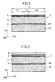
- FIG. 1 represents a view in longitudinal section of a semiconductor wafer in which this invention is to be implemented.
- FIG. 2 represents a view of this plate in longitudinal section after deposition of a delimitation layer.
- FIG. 3 represents a top view of this plate after an etching of the delimitation layer and a first attack of the plate.
- Figures 4 and 5 show two views of this plate in section along two transverse planes IV-IV and V-V of Figure 3 after this first attack.
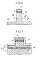
- Figures 6 and 7 show two views of this plate in section along the same two transverse planes after a second attack.
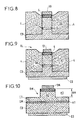
- FIG. 8 represents a view of this plate in section through the transverse plane IV-IV after filling of lateral recesses.
- Figures 9 and 10 show two views of this plate in section through the same two transverse planes after the formation of electrodes, this plate then constituting a device according to the invention.
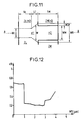
- FIG. 11 represents a top view of a composite guide of this device.
- FIG. 12 represents a diagram of the variation of a loss of light in this device as a function of an excess of width of a guide segment of this device.
- FIGS. 1 to 10 we will first of all indicate how an underground ribbon and an external ribbon of this device can be produced, it being understood that these ribbons constitute two different guiding structures and that these two structures must be mutually connected. so as to constitute a rear part and a front segment of an optical guide according to the invention.
- a device to be manufactured is formed in a substrate 2.
- the latter is for example, consisting of a semiconductor wafer 2 formed of layers extending in a horizontal longitudinal direction DZ and a transverse direction DX and superimposed in a vertical direction DY. These directions are defined with respect to this brochure.
- This plate includes a buried ribbon segment SL, a transition segment ST extending the segment SL, and an external ribbon segment SM extending and succeeding in the longitudinal direction and comprising respectively a buried ribbon RL and an external ribbon RM. These ribbons are shown in Figures 9 and 10. The two segments are mutually aligned in the direction DZ.
- Each of them has an increased index GL or GM layer located between two confinement layers, one lower CB and the other upper CS.
- the increased index considered here is a refractive index n 1 and it is increased compared to that of the confinement layers so as to limit the vertical extension of a single guided mode according to which an optical wave must propagate longitudinally in this ribbon.
- the layer with increased index GL and the upper confinement layer CS of the buried ribbon RL are limited transversely between two lateral confinement blocks 4 forming parts of the wafer 2.
- These blocks have a refractive index n 2 lower than said increased index so that this transverse limitation of the increased index layer limits the transverse extension of the mode guided by this ribbon. They are also produced so as to confine in the buried ribbon a supply current flowing vertically in the wafer. This can be obtained in a known manner by increasing the electrical resistivity of a material constituting these blocks, and / or by the formation of a blocking semiconductor junction in these blocks.
- the upper confinement layer CS of the outer tape RM has a refractive index n 2 greater than the index n 3 of a space, for example gaseous, outside the wafer. It is limited transversely between two recesses 14 and 16 of the plate belonging to this outside space and leaving the layer with increased index GM and the lower confinement layer CB remaining. This transverse limitation of the upper confinement layer limits the transverse extension of the mode guided by this ribbon.
- the substrate and the lower confinement layer are for example of the n type.
- the upper confinement layer CH is for example of the p type as well as a heavily doped contact layer 6 which has been deposited on this confinement layer.
- the device to be manufactured also includes electrodes EL, EM and EG formed above and below the wafer in each of the segments. More precisely, the electrodes EL and EM are respectively formed on the buried ribbon RL and on the external ribbon RM and the lower electrode EG is common to the two segments.
- the etching of the delimitation layer is carried out to also form the delimitation strip 10 in the buried ribbon segment SL by making this strip transversely coincide with the buried ribbon RL to be formed. It follows that the first attack then releases in this first segment a primer of buried ribbon 12. This primer is shown in FIG. 4. It projects between the two initial lateral recesses 14 and 16 which are limited in depth below the GL increased index layer.
- the lateral confinement blocks can be formed by depositing a succession of materials different from each other.
- the boundary 10 and protective 18 layers are typically made of dielectric materials. An operation of at least partial elimination of the remaining parts of the delimitation and protection layers is then carried out after the deposition of the lateral confinement material 4 and before the formation of the upper electrodes EL and EM.
- the confinement layers CB and CS for example consist of indium phosphide Inp, the layer with increased index GL, GM of ternary or quaternary alloys such as Ga In AS, Ga In As P, or of a well overlay quantum formed by such alloys and separated by indium phosphide barriers, the delimiting layer 10 of silicon nitride Si3N4 and the protective layer 18 of silica SiO2, at least one lateral confinement material 4 being constituted for example of semi-insulating indium phosphide.
- GM has two different characteristic wavelengths such as 1560 and 1510 nm respectively in the two segments SL and SM so that the buried ribbon segment SL constitutes a laser for emitting infrared light and that the external ribbon segment SM constitutes a modulator for modulating this light.
- the present invention makes it possible to connect with a minimum of losses two guide segments such as the buried and external ribbons previously described.
- this guide generally relates to an optical guide, this guide comprising in a monolithic manner a rear part SL, ST and a front segment SM extending and succeeding one another in a length of this guide by connecting in a zone of connection, this guide having at each point of its length a width W and a lateral confinement factor V, this factor being constituted by the ratio of a confined optical power in this width at a total optical power, these optical powers being those of the same light guided by this guide, this factor being greater in this rear part than in this front segment in the vicinity of this connection zone, this guide being characterized by the fact that this width is also greater in this rear part than in this front segment in the vicinity of this connection zone.
- the abscissae x being defined in the transverse direction DX
- E designating the optical electric field of the guided light
- width W corresponding to a single-mode guidance this factor increases with this width. It also increases with the thickness of the ribbon and with an index difference constituted by the difference between the ribbon index and the lateral confinement index.
- Said rear portion typically includes, as shown in FIG. 11, a rear segment SL and a transition segment ST connecting this rear segment to said front segment SM, a direct direction DX being defined from this rear segment to this front segment, the width of the guide having a first WL value in the rear segment and a second WM value greater than the first in the front segment.
- the width of the guide gradually increases in the transition segment in the direct direction from this first value up to a maximum value WK reached in the vicinity of the connection area and greater than this second value.
- the guide has, at least in the vicinity of the connection zone, a symmetry with respect to a longitudinal plane A.
- the guide is formed in each part of its length by a set of superimposed layers such as CB, GL, CS in the rear part and CB, GM, CS, 6 , 10 in the front segment, these layers having respective thicknesses.
- At least one of these overlapping layers includes a ribbon such as GL in the rear segment and RM in the front segment.
- This ribbon extends along the length of the guide over the thickness of this layer, having a limited width. It has a refractive index constituting a ribbon index and it is surrounded laterally by lateral confinement zones such as 4 in the rear segment and 14 and 16 in the front segment. These zones have refractive indices constituting confinement indices.
- the width of the guide is an effective ribbon width defined in an assembly comprising at least one layer and constituted by the layer or layers including said ribbons.
- the guide presents a confinement configuration in each transverse plane passing through a point of its length. This configuration is that of said layers, ribbons, and confinement zones with their thicknesses and their refractive indices, with the exception of the width of the guide. It is uniform on the one hand in the rear part of the guide, on the other hand in the front segment and it is such that the lateral confinement factor is greater in the rear segment than in the front segment. Typically the rear part connects directly to the front segment.
- the optical guide is always monomodal for guided light having a wavelength of 1550 nm.
- the rear segment SL has a homogeneous core which is formed by the layer GL and which has the refractive index n 1 .
- the width of the guide is the width WM of the external strip RM.
- a vertical confinement factor is essentially defined by the thickness HL of the GM layer and by an index difference between this layer and the adjacent layers.
- the confinement factor in the transverse direction DX essentially depends on the thickness HL and the difference in index ⁇ nL.
- the width of the ribbon GL in this segment constitutes the width of the guide. It increases in the direct direction, for example linearly, from WL up to a maximum width WK greater than WM.
- the loss of light on passing between the segments SL and SM decreases when the length L of the transition segment ST increases. This length must however be limited to avoid excessive bulk of the manufactured device. In the case of a semiconductor modulator laser assembly as given in example, it seems to be understood to be between 100 and 500 ⁇ m.
- This variation is represented in FIG. 12, the values of the loss being plotted on the ordinate in decibels, and the excess width WD being plotted on the abscissa in micrometers.
- the half excess width WD should preferably be included in a range extending from 1 to 3 ⁇ m.
- this excess is between 0.1 ⁇ m and 30 ⁇ m.
- the point of change of width where the reduction in width is located. of the guide is slightly offset forwards or backwards relative to the point of change of confinement where the reduction of the confinement factor is located. This reduction in the width of the guide could also be progressive.
- the guide according to the invention is typically included in a device for treating guided light in this guide.
- the light to be treated can propagate in the longitudinal direction in said direct direction or in the opposite direction.
- the treatment carried out may consist in generating and modulating this light. More generally, it involves carrying out two successive operations concerning this light, one being carried out in the rear segment, the other in the front segment, the difference between the confinement configurations of these two segments being made necessary by the respective natures. of these two operations.
Landscapes
- Physics & Mathematics (AREA)
- General Physics & Mathematics (AREA)
- Optics & Photonics (AREA)
- Engineering & Computer Science (AREA)
- Condensed Matter Physics & Semiconductors (AREA)
- Electromagnetism (AREA)
- Power Engineering (AREA)
- Microelectronics & Electronic Packaging (AREA)
- Optical Integrated Circuits (AREA)
- Semiconductor Lasers (AREA)
Applications Claiming Priority (2)
| Application Number | Priority Date | Filing Date | Title |
|---|---|---|---|
| FR9502045A FR2730821B1 (fr) | 1995-02-22 | 1995-02-22 | Guide optique segmente pouvant notamment etre inclus dans un dispositif semiconducteur |
| FR9502045 | 1995-02-22 |
Publications (2)
| Publication Number | Publication Date |
|---|---|
| EP0729042A1 true EP0729042A1 (de) | 1996-08-28 |
| EP0729042B1 EP0729042B1 (de) | 2002-12-18 |
Family
ID=9476400
Family Applications (1)
| Application Number | Title | Priority Date | Filing Date |
|---|---|---|---|
| EP96400337A Expired - Lifetime EP0729042B1 (de) | 1995-02-22 | 1996-02-19 | Segmentierter optischer Leiter, dessen Verwendung insbesondere in einer Halbleitervorrichtung |
Country Status (6)
| Country | Link |
|---|---|
| US (1) | US5687272A (de) |
| EP (1) | EP0729042B1 (de) |
| JP (1) | JPH08248248A (de) |
| CA (1) | CA2170005C (de) |
| DE (1) | DE69625396T2 (de) |
| FR (1) | FR2730821B1 (de) |
Cited By (6)
| Publication number | Priority date | Publication date | Assignee | Title |
|---|---|---|---|---|
| GB2334789A (en) * | 1998-06-12 | 1999-09-01 | Bookham Technology Ltd | Waveguide end face |
| FR2779834A1 (fr) * | 1998-06-15 | 1999-12-17 | Alsthom Cge Alcatel | Composant monolithique electro-optique multi-sections |
| WO2001095446A1 (en) * | 2000-06-08 | 2001-12-13 | Nichia Corporation | Semiconductor laser device, and method of manufacturing the same |
| GB2366394A (en) * | 2000-08-11 | 2002-03-06 | Kymata Ltd | Integrated optical device with cladding having mesa formation |
| RU2262171C2 (ru) * | 2000-06-08 | 2005-10-10 | Нития Корпорейшн | Полупроводниковое лазерное устройство и способ его изготовления |
| EP2277068A4 (de) * | 2007-06-27 | 2014-05-21 | Syntune Ab | Übergangselement für optische wellenleiter |
Families Citing this family (15)
| Publication number | Priority date | Publication date | Assignee | Title |
|---|---|---|---|---|
| JPH1075011A (ja) * | 1996-08-30 | 1998-03-17 | Sony Corp | 半導体レーザ |
| FR2760850B1 (fr) * | 1997-03-13 | 1999-04-16 | Alsthom Cge Alcatel | Procede de fabrication de circuits optiques integres permettant de minimiser les pertes optiques de couplage |
| US5917967A (en) * | 1997-05-21 | 1999-06-29 | The United States Of America As Represented By The Secretary Of The Army | Techniques for forming optical electronic integrated circuits having interconnects in the form of semiconductor waveguides |
| KR100265795B1 (ko) * | 1997-11-18 | 2000-09-15 | 윤종용 | 광도파로칩 |
| SE522417C2 (sv) * | 1998-10-15 | 2004-02-10 | Ericsson Telefon Ab L M | Elektro-absorptionsmodulator (EAM) samt förfarande för tillverkning av sådan modulator |
| US6600764B1 (en) * | 2000-01-20 | 2003-07-29 | Trump Photonics Inc. | High power single mode semiconductor laser |
| DE60135242D1 (de) * | 2000-10-27 | 2008-09-18 | Pirelli & C Spa | Hybride planare vergrabene / steg-wellenleiter |
| US6643048B2 (en) * | 2000-11-03 | 2003-11-04 | Codeon Corporation | Low-loss electrode structures using resistive connections for optical modulation applications |
| US6539150B2 (en) * | 2000-12-13 | 2003-03-25 | Alcatel Optronics Uk Limited | Segmented waveguide flattening the passband of a phasar |
| JP4320167B2 (ja) * | 2002-12-12 | 2009-08-26 | 忠弘 大見 | 半導体素子及びシリコン酸化窒化膜の製造方法 |
| KR100596509B1 (ko) * | 2004-11-18 | 2006-07-05 | 한국전자통신연구원 | 봉우리형 도파로 집적 반도체 광소자의 제조방법 |
| JP2011258785A (ja) * | 2010-06-10 | 2011-12-22 | Nippon Telegr & Teleph Corp <Ntt> | 光導波路およびそれを用いた光半導体装置 |
| US10985532B2 (en) | 2016-10-27 | 2021-04-20 | Mitsubishi Electric Corporation | Semiconductor optical waveguide and optical integrated element |
| JP2020174140A (ja) * | 2019-04-11 | 2020-10-22 | 住友電気工業株式会社 | 半導体集積光デバイス、半導体集積光デバイスを作製する方法 |
| WO2025215742A1 (ja) * | 2024-04-09 | 2025-10-16 | 三菱電機株式会社 | 光半導体装置 |
Citations (1)
| Publication number | Priority date | Publication date | Assignee | Title |
|---|---|---|---|---|
| EP0583679A1 (de) * | 1992-08-14 | 1994-02-23 | Siemens Aktiengesellschaft | Anordnung zur Umwandlung einer optischen Welle relativ kleineren Querschnitts in eine optische Welle relativ grösseren Querschnitts |
Family Cites Families (6)
| Publication number | Priority date | Publication date | Assignee | Title |
|---|---|---|---|---|
| US4913506A (en) * | 1988-02-26 | 1990-04-03 | Kokusai Denshin Denwa Kabushiki Kaisha | Optical modulation device |
| US5078516A (en) * | 1990-11-06 | 1992-01-07 | Bell Communications Research, Inc. | Tapered rib waveguides |
| EP0495202B1 (de) * | 1991-01-15 | 1996-04-24 | Siemens Aktiengesellschaft | Anordnung zum Umwandeln einer optischen Welle kleiner Fleckweite in eine Welle grösserer Fleckweite |
| EP0532816B1 (de) * | 1991-09-19 | 1995-08-09 | International Business Machines Corporation | Selbstjustierender optischer Wellenleiter-Laser, Struktur und dessen Herstellungsverfahren |
| US5515464A (en) * | 1992-07-06 | 1996-05-07 | Sheem Sang K | Optical fiber interconnections using self-aligned core-extensions |
| JP2982619B2 (ja) * | 1994-06-29 | 1999-11-29 | 日本電気株式会社 | 半導体光導波路集積型受光素子 |
-
1995
- 1995-02-22 FR FR9502045A patent/FR2730821B1/fr not_active Expired - Lifetime
-
1996
- 1996-02-16 US US08/602,380 patent/US5687272A/en not_active Expired - Lifetime
- 1996-02-19 DE DE69625396T patent/DE69625396T2/de not_active Expired - Lifetime
- 1996-02-19 EP EP96400337A patent/EP0729042B1/de not_active Expired - Lifetime
- 1996-02-21 CA CA002170005A patent/CA2170005C/fr not_active Expired - Fee Related
- 1996-02-22 JP JP8035199A patent/JPH08248248A/ja active Pending
Patent Citations (1)
| Publication number | Priority date | Publication date | Assignee | Title |
|---|---|---|---|---|
| EP0583679A1 (de) * | 1992-08-14 | 1994-02-23 | Siemens Aktiengesellschaft | Anordnung zur Umwandlung einer optischen Welle relativ kleineren Querschnitts in eine optische Welle relativ grösseren Querschnitts |
Non-Patent Citations (3)
| Title |
|---|
| J.-M.CHEONG ET.AL.: "High alignment tolerance coupling scheme for multichannel laser diode/singlemode fibre modules using a tapered waveguide array", ELECTRONICS LETTERS., vol. 30, no. 18, 1 September 1994 (1994-09-01), ENAGE GB, pages 1515 - 1516, XP002004299 * |
| M.SUZUKI ET.AL.: "Monolithic integration of InGaAsP/InP", JOURNAL OF LIGHTWAVE TECHNOLOGY., vol. 5, no. 9, September 1987 (1987-09-01), NEW YORK US, pages 1277 - 1285, XP002004301 * |
| O.MITOMI ET.AL.: "Design of a single-mode tapered waveguide for low-loss chip-to-fiber coupling", IEEE JOURNAL OF QUANTUM ELECTRONICS., vol. 30, no. 8, August 1994 (1994-08-01), NEW YORK US, pages 1787 - 1793, XP002004300 * |
Cited By (15)
| Publication number | Priority date | Publication date | Assignee | Title |
|---|---|---|---|---|
| GB2334789A (en) * | 1998-06-12 | 1999-09-01 | Bookham Technology Ltd | Waveguide end face |
| GB2334789B (en) * | 1998-06-12 | 2000-01-19 | Bookham Technology Ltd | A waveguide end face |
| US6266468B1 (en) | 1998-06-12 | 2001-07-24 | Bookham Technology Plc | Waveguide end face |
| FR2779834A1 (fr) * | 1998-06-15 | 1999-12-17 | Alsthom Cge Alcatel | Composant monolithique electro-optique multi-sections |
| EP0966076A1 (de) * | 1998-06-15 | 1999-12-22 | Alcatel | Aus mehreren Abschnitten bestehendes elektrooptisches monolithisches Bauelement |
| US6236794B1 (en) | 1998-06-15 | 2001-05-22 | Alcatel | Multi-section electro-optical monolithic component |
| WO2001095446A1 (en) * | 2000-06-08 | 2001-12-13 | Nichia Corporation | Semiconductor laser device, and method of manufacturing the same |
| US6925101B2 (en) | 2000-06-08 | 2005-08-02 | Nichia Corporation | Semiconductor laser device, and method of manufacturing the same |
| RU2262171C2 (ru) * | 2000-06-08 | 2005-10-10 | Нития Корпорейшн | Полупроводниковое лазерное устройство и способ его изготовления |
| CN100375349C (zh) * | 2000-06-08 | 2008-03-12 | 日亚化学工业株式会社 | 半导体激光元件及其制造方法 |
| US7470555B2 (en) | 2000-06-08 | 2008-12-30 | Nichia Corporation | Semiconductor laser device, and method of manufacturing the same |
| US7709281B2 (en) | 2000-06-08 | 2010-05-04 | Nichia Corporation | Semiconductor laser device and method of manufacturing the same |
| GB2366394A (en) * | 2000-08-11 | 2002-03-06 | Kymata Ltd | Integrated optical device with cladding having mesa formation |
| US7054516B2 (en) | 2000-08-11 | 2006-05-30 | Russell Childs | Integrated optical device |
| EP2277068A4 (de) * | 2007-06-27 | 2014-05-21 | Syntune Ab | Übergangselement für optische wellenleiter |
Also Published As
| Publication number | Publication date |
|---|---|
| US5687272A (en) | 1997-11-11 |
| FR2730821A1 (fr) | 1996-08-23 |
| FR2730821B1 (fr) | 1997-04-30 |
| DE69625396D1 (de) | 2003-01-30 |
| DE69625396T2 (de) | 2003-08-21 |
| CA2170005C (fr) | 2000-05-30 |
| EP0729042B1 (de) | 2002-12-18 |
| JPH08248248A (ja) | 1996-09-27 |
| CA2170005A1 (fr) | 1996-08-23 |
Similar Documents
| Publication | Publication Date | Title |
|---|---|---|
| CA2170005C (fr) | Guide optique segmente pouvant notamment etre inclus dans un dispositif semiconducteur | |
| EP0545820B1 (de) | Optisches Halbleiterbauelement mit einer grösseren Ausgangsfeldfleckverteilung und sein Herstellungsverfahren | |
| EP0742620B1 (de) | Halbleiterlaser | |
| EP0179507B1 (de) | Koppler zwischen Wellenleitern, monolithbar auf einem Halbleitersubstrat integriert | |
| FR2728399A1 (fr) | Composant laser a reflecteur de bragg en materiau organique et procede pour sa realisation | |
| EP0091859B1 (de) | Verfahren zur Herstellung eines Halbleiterlasers mit mehreren unabhängigen Wellenlängen | |
| FR2596529A1 (fr) | Guide d'onde optique en materiau semiconducteur, laser appliquant ce guide d'onde et procede de realisation | |
| FR2729789A1 (fr) | Detecteur a puits quantique et procede de realisation | |
| EP0642041B1 (de) | Aktives optisches Halbleiter-Stegwellenleiterelement | |
| FR2650399A1 (fr) | Dispositif semiconducteur incluant un coupleur directionnel pour les composantes te, tm | |
| EP0700136B1 (de) | Verfahren zur Ausrichtung eines vergrabenen Streifenleiters und eines externen Streifenleiters in einem optischen Halbleiterbauelement | |
| EP0310184B1 (de) | Optisches Schaltelement aus zwei parallelen Lichtleitern und aus solchen Elementen zusammengesetzte Schaltmatrix | |
| FR3085369A1 (fr) | Modulateur electro-optique | |
| EP0370577B1 (de) | Integrierte Halbleiter-Vorrichtung mit einem optoelektronischen Schaltelement | |
| EP0651477B1 (de) | Integrierte oberflächenemittierende Laservorrichtung | |
| EP0274796B1 (de) | Optisches Lichtwellenleiter-Schaltelement und aus derartigen Elementen gebildete Schaltmatrix | |
| FR2888410A1 (fr) | Dispositif optique a source laser semi-conducteur et isolateur optique integres | |
| WO2002017453A1 (fr) | Amplificateur optique en semi-conducteur | |
| FR2683392A1 (fr) | Procede de realisation de composants optoelectroniques par epitaxie selective dans un sillon. | |
| WO2002017452A1 (fr) | Dispositif optique amplificateur | |
| WO2025008545A1 (fr) | Puce photonique à structure hétérogène de semi-conducteur iii-v sur un deuxième semi-conducteur | |
| FR2854469A1 (fr) | Procede de fabrication d'un dispositif optique semi-conducteur comportant une region munie d'une couche active a epaisseur variable | |
| WO2002017454A1 (fr) | Amplificateur optique a semi-conducteur |
Legal Events
| Date | Code | Title | Description |
|---|---|---|---|
| PUAI | Public reference made under article 153(3) epc to a published international application that has entered the european phase |
Free format text: ORIGINAL CODE: 0009012 |
|
| AK | Designated contracting states |
Kind code of ref document: A1 Designated state(s): DE ES GB IT NL SE |
|
| 17P | Request for examination filed |
Effective date: 19970121 |
|
| 17Q | First examination report despatched |
Effective date: 20010831 |
|
| GRAG | Despatch of communication of intention to grant |
Free format text: ORIGINAL CODE: EPIDOS AGRA |
|
| RIC1 | Information provided on ipc code assigned before grant |
Free format text: 7G 02B 6/30 A, 7G 02B 6/12 B, 7H 01S 5/02 B |
|
| GRAG | Despatch of communication of intention to grant |
Free format text: ORIGINAL CODE: EPIDOS AGRA |
|
| GRAH | Despatch of communication of intention to grant a patent |
Free format text: ORIGINAL CODE: EPIDOS IGRA |
|
| GRAH | Despatch of communication of intention to grant a patent |
Free format text: ORIGINAL CODE: EPIDOS IGRA |
|
| GRAA | (expected) grant |
Free format text: ORIGINAL CODE: 0009210 |
|
| RAP1 | Party data changed (applicant data changed or rights of an application transferred) |
Owner name: ALCATEL |
|
| AK | Designated contracting states |
Kind code of ref document: B1 Designated state(s): DE ES GB IT NL SE |
|
| PG25 | Lapsed in a contracting state [announced via postgrant information from national office to epo] |
Ref country code: NL Free format text: LAPSE BECAUSE OF FAILURE TO SUBMIT A TRANSLATION OF THE DESCRIPTION OR TO PAY THE FEE WITHIN THE PRESCRIBED TIME-LIMIT Effective date: 20021218 |
|
| REG | Reference to a national code |
Ref country code: GB Ref legal event code: FG4D Free format text: NOT ENGLISH |
|
| GBT | Gb: translation of ep patent filed (gb section 77(6)(a)/1977) |
Effective date: 20021218 |
|
| REF | Corresponds to: |
Ref document number: 69625396 Country of ref document: DE Date of ref document: 20030130 Kind code of ref document: P Ref document number: 69625396 Country of ref document: DE Date of ref document: 20030130 |
|
| PG25 | Lapsed in a contracting state [announced via postgrant information from national office to epo] |
Ref country code: SE Free format text: LAPSE BECAUSE OF FAILURE TO SUBMIT A TRANSLATION OF THE DESCRIPTION OR TO PAY THE FEE WITHIN THE PRESCRIBED TIME-LIMIT Effective date: 20030318 |
|
| PG25 | Lapsed in a contracting state [announced via postgrant information from national office to epo] |
Ref country code: ES Free format text: LAPSE BECAUSE OF FAILURE TO SUBMIT A TRANSLATION OF THE DESCRIPTION OR TO PAY THE FEE WITHIN THE PRESCRIBED TIME-LIMIT Effective date: 20030627 |
|
| PLBE | No opposition filed within time limit |
Free format text: ORIGINAL CODE: 0009261 |
|
| STAA | Information on the status of an ep patent application or granted ep patent |
Free format text: STATUS: NO OPPOSITION FILED WITHIN TIME LIMIT |
|
| 26N | No opposition filed |
Effective date: 20030919 |
|
| REG | Reference to a national code |
Ref country code: GB Ref legal event code: 732E |
|
| PGFP | Annual fee paid to national office [announced via postgrant information from national office to epo] |
Ref country code: DE Payment date: 20130213 Year of fee payment: 18 Ref country code: GB Payment date: 20130213 Year of fee payment: 18 |
|
| PGFP | Annual fee paid to national office [announced via postgrant information from national office to epo] |
Ref country code: IT Payment date: 20140219 Year of fee payment: 19 |
|
| REG | Reference to a national code |
Ref country code: GB Ref legal event code: 732E Free format text: REGISTERED BETWEEN 20140612 AND 20140618 |
|
| REG | Reference to a national code |
Ref country code: DE Ref legal event code: R119 Ref document number: 69625396 Country of ref document: DE |
|
| GBPC | Gb: european patent ceased through non-payment of renewal fee |
Effective date: 20140219 |
|
| REG | Reference to a national code |
Ref country code: DE Ref legal event code: R119 Ref document number: 69625396 Country of ref document: DE Effective date: 20140902 |
|
| PG25 | Lapsed in a contracting state [announced via postgrant information from national office to epo] |
Ref country code: GB Free format text: LAPSE BECAUSE OF NON-PAYMENT OF DUE FEES Effective date: 20140219 Ref country code: DE Free format text: LAPSE BECAUSE OF NON-PAYMENT OF DUE FEES Effective date: 20140902 |
|
| PG25 | Lapsed in a contracting state [announced via postgrant information from national office to epo] |
Ref country code: IT Free format text: LAPSE BECAUSE OF NON-PAYMENT OF DUE FEES Effective date: 20150219 |