EP0545820B1 - Optisches Halbleiterbauelement mit einer grösseren Ausgangsfeldfleckverteilung und sein Herstellungsverfahren - Google Patents
Optisches Halbleiterbauelement mit einer grösseren Ausgangsfeldfleckverteilung und sein Herstellungsverfahren Download PDFInfo
- Publication number
- EP0545820B1 EP0545820B1 EP92403264A EP92403264A EP0545820B1 EP 0545820 B1 EP0545820 B1 EP 0545820B1 EP 92403264 A EP92403264 A EP 92403264A EP 92403264 A EP92403264 A EP 92403264A EP 0545820 B1 EP0545820 B1 EP 0545820B1
- Authority
- EP
- European Patent Office
- Prior art keywords
- mode
- transition
- waveguide
- width
- section
- Prior art date
- Legal status (The legal status is an assumption and is not a legal conclusion. Google has not performed a legal analysis and makes no representation as to the accuracy of the status listed.)
- Expired - Lifetime
Links
Images


Classifications
-
- G—PHYSICS
- G02—OPTICS
- G02B—OPTICAL ELEMENTS, SYSTEMS OR APPARATUS
- G02B6/00—Light guides; Structural details of arrangements comprising light guides and other optical elements, e.g. couplings
- G02B6/24—Coupling light guides
- G02B6/26—Optical coupling means
- G02B6/30—Optical coupling means for use between fibre and thin-film device
- G02B6/305—Optical coupling means for use between fibre and thin-film device and having an integrated mode-size expanding section, e.g. tapered waveguide
-
- H—ELECTRICITY
- H01—ELECTRIC ELEMENTS
- H01S—DEVICES USING THE PROCESS OF LIGHT AMPLIFICATION BY STIMULATED EMISSION OF RADIATION [LASER] TO AMPLIFY OR GENERATE LIGHT; DEVICES USING STIMULATED EMISSION OF ELECTROMAGNETIC RADIATION IN WAVE RANGES OTHER THAN OPTICAL
- H01S5/00—Semiconductor lasers
- H01S5/10—Construction or shape of the optical resonator, e.g. extended or external cavity, coupled cavities, bent-guide, varying width, thickness or composition of the active region
- H01S5/1028—Coupling to elements in the cavity, e.g. coupling to waveguides adjacent the active region, e.g. forward coupled [DFC] structures
- H01S5/1032—Coupling to elements comprising an optical axis that is not aligned with the optical axis of the active region
-
- H—ELECTRICITY
- H01—ELECTRIC ELEMENTS
- H01S—DEVICES USING THE PROCESS OF LIGHT AMPLIFICATION BY STIMULATED EMISSION OF RADIATION [LASER] TO AMPLIFY OR GENERATE LIGHT; DEVICES USING STIMULATED EMISSION OF ELECTROMAGNETIC RADIATION IN WAVE RANGES OTHER THAN OPTICAL
- H01S5/00—Semiconductor lasers
- H01S5/10—Construction or shape of the optical resonator, e.g. extended or external cavity, coupled cavities, bent-guide, varying width, thickness or composition of the active region
- H01S5/1003—Waveguide having a modified shape along the axis, e.g. branched, curved, tapered, voids
- H01S5/1014—Tapered waveguide, e.g. spotsize converter
-
- H—ELECTRICITY
- H01—ELECTRIC ELEMENTS
- H01S—DEVICES USING THE PROCESS OF LIGHT AMPLIFICATION BY STIMULATED EMISSION OF RADIATION [LASER] TO AMPLIFY OR GENERATE LIGHT; DEVICES USING STIMULATED EMISSION OF ELECTROMAGNETIC RADIATION IN WAVE RANGES OTHER THAN OPTICAL
- H01S5/00—Semiconductor lasers
- H01S5/10—Construction or shape of the optical resonator, e.g. extended or external cavity, coupled cavities, bent-guide, varying width, thickness or composition of the active region
- H01S5/1053—Comprising an active region having a varying composition or cross-section in a specific direction
- H01S5/1064—Comprising an active region having a varying composition or cross-section in a specific direction varying width along the optical axis
-
- H—ELECTRICITY
- H01—ELECTRIC ELEMENTS
- H01S—DEVICES USING THE PROCESS OF LIGHT AMPLIFICATION BY STIMULATED EMISSION OF RADIATION [LASER] TO AMPLIFY OR GENERATE LIGHT; DEVICES USING STIMULATED EMISSION OF ELECTROMAGNETIC RADIATION IN WAVE RANGES OTHER THAN OPTICAL
- H01S5/00—Semiconductor lasers
- H01S5/20—Structure or shape of the semiconductor body to guide the optical wave ; Confining structures perpendicular to the optical axis, e.g. index or gain guiding, stripe geometry, broad area lasers, gain tailoring, transverse or lateral reflectors, special cladding structures, MQW barrier reflection layers
- H01S5/22—Structure or shape of the semiconductor body to guide the optical wave ; Confining structures perpendicular to the optical axis, e.g. index or gain guiding, stripe geometry, broad area lasers, gain tailoring, transverse or lateral reflectors, special cladding structures, MQW barrier reflection layers having a ridge or stripe structure
- H01S5/227—Buried mesa structure ; Striped active layer
Definitions
- the present invention relates both to the production of a semiconductor optical component and to its coupling to an optical element which is external to it. More specifically, it tends to solve a known problem which is to obtain two results simultaneously.
- a first result to be obtained is to "treat” a light efficiently in the optical component considered, the word “treat” here designating actions such as emitting, amplifying, detecting or modulating this light. It will often be considered below, by way of a typical although non-limiting example, and to facilitate understanding of the present invention, that the optical component in which this light is treated is a laser.
- the light to be treated then takes the form of a wave guided in this laser according to a so-called narrow mode, the size of which can be limited by considerations linked to the search for efficiency and to the internal functioning of this laser.
- the second result to be obtained is that the light which is thus treated is supplied to said external optical element or can be effectively received from this element in the form of a wave guided in an enlarged mode having a size larger than this narrow mode.
- such an extended mode has the advantage of allowing easier and more efficient coupling of this wave with an optical fiber which receives or supplies the light treated or to be treated.
- This document describes a semiconductor laser transmitter providing a guided output wave in an expanded mode.
- the realization of this laser is complex.
- This document describes a coupling device which receives a wave in a narrow mode at the output of a semiconductor laser transmitter and which transmits it in an expanded mode facilitating coupling to an optical fiber.
- the object of the present invention is in particular to propose for this problem a solution which is simple to carry out, which requires only a limited space, and which only causes small losses of light.
- the optical component according to the invention is defined by claim 1 and a manufacturing method according to the invention is defined by claim 13.
- FIG. 1 represents a view of a first laser in section along a transverse plane I-I of FIG. 2.
- FIG. 2 represents a view of this first laser in section partial along a longitudinal plane II-II of FIG. 1.
- FIG. 3 represents a view of this first laser in partial section along a horizontal plane III-III of FIG. 1.
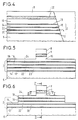
- Figures 4, 5 and 6 show views of this first laser in section along the transverse plane I-I at successive stages in the manufacture of this laser.
- FIG. 7 represents a view of a second laser according to this invention, in section along a transverse plane VII-VII of FIG. 8.
- FIG. 8 represents a view of this second laser according to this invention, in partial section along a longitudinal plane VIII-VIII of FIG. 7.
- FIG. 9 represents a view of this second laser in partial section along a horizontal plane IX - IX of FIG. 7.
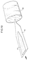
- FIG. 10 represents a partial perspective view of this second laser.
- This plate defines two longitudinal X and transverse Y directions. Horizontal planes extend in these two directions. Transversal planes are perpendicular to this longitudinal direction. This plate also defines a vertical direction Z perpendicular to these horizontal planes. Lengths, widths, thicknesses and transverse areas of elements internal to this plate will be measured in these longitudinal, transverse and vertical directions and in these transverse planes, respectively.
- This plate has three successive sections SA, SB, SC (FIG. 2) which extend and succeed one another longitudinally and which constitute at least one processing section SA and one mode transition section SB.
- the processing section SA more particularly constitutes an amplification section.
- This section begins at an initial transition point PA in the vicinity of the amplification section and ends at a wide mode point PB which at the same time constitutes, in this first laser, a remote endpoint of this section.
- a third section of this first laser constitutes a coupling section SC from which the laser can be coupled to an optical fiber.
- two longitudinally extreme faces (not shown) of this plate can constitute reflectors for producing a laser transmitter. They could also be treated to avoid the reflection of light and constitute a laser amplifier which would be coupled to two optical fibers of entry and exit and which would include for this two sections of transition of mode and two sections of coupling of share and d other from the amplification section.
- the propagation of the light according to the narrow mode allows its effective amplification and possibly little sensitive to its polarization in the amplification section.
- the wide mode facilitates coupling to an optical fiber.
- the wafer 4 also essentially comprises an upper confinement layer 8 having a second type of conductivity opposite to the first so that the passage of an electric supply current in a direct direction between these lower and upper confinement layers is accompanied by the injection of said charge carriers of opposite types into the active guide 1 in the amplification section SA.
- the complementary material 32 comprises various well-known layers which are useful for the operation of the laser. and who are not represented. These are in particular the lateral layers of optical and electrical confinement, contact layers, etc. Furthermore, the wafer is provided with electrodes, not shown, to enable the electrical supply current to be injected.
- the passive guide 2 In the amplification section SA or at least at the initial transition point, the passive guide 2 has a width called "normal" which is greater than or equal to the width of the active guide 1. It also has a thickness which is greater than or equal and an average refractive index which is less than the thickness and the refractive index presented by this active guide, respectively. More precisely, the average index of the passive guide is chosen sufficiently close to that of the surrounding material so that the narrow mode is essentially guided by the active guide in the SA section.
- the wide mode point PB constitutes one end of the active guide 1.
- the wide mode MC has transverse and vertical sizes greater than 200% and preferably 400% of transverse and vertical sizes of the narrow mode MA. These sizes of each of these modes are conventionally defined as the transverse and vertical dimensions of the domain in which the electric field of this mode is weakened in a ratio less than 2.718 with respect to the maximum electric field of this mode, respectively.
- a separation layer 10 is preferably interposed between the two active guides 1 and passive 2. It has a lower refractive index than the average refractive index of each of these two guides. Its thickness constitutes a separation thickness which is chosen to be large enough to allow the active guide to be transversely limited, that is to say to define its width, by an etching operation, while avoiding the risk that this etching operation reaches the passive guide, which in the transition section must be wider for reasons which will appear below. This thickness is at the same time chosen to be small enough to maintain the necessary optical coupling between the active and passive guides.
- the active guide 1 has, in the mode transition section SB and in projection on a horizontal plane, the general shape of a point with cut end 28, that is to say that its width is gradually reduced until a final width sufficiently small so that its influence on the mode of propagation of the light becomes negligible compared to that of the guide 2.
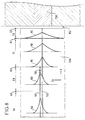
- FIGS. 2 and 3 which very roughly represent diagrams of energy distributions corresponding to the narrow mode MA , to an intermediate distribution MB and to the wide mode MC. Each of these distributions is represented by two diagrams, one in FIG. 2 and the other in FIG. 3. Each of these diagrams has a curve and a reference axis.
- This reference axis represents a line of a transverse vertical plane passing through the plate 4, this line passing through the point of this plane where the value of the alternating electric field of the guided optical mode is maximum.
- this line we determine the value of this electric field and the square of this value is plotted parallel to the longitudinal direction X to mark a point on the curve of this diagram.
- the decrease in the width of the guide 1 causes a reduction in the confinement of the optical mode guided in the guide 1 as well as a progressive "sliding" of this mode towards the guide 2.
- This sliding is accompanied by a dilation due to the lower average refractive index of the guide 2.
- the length of the decay zone must be sufficient to ensure the desired smallness of the transition losses (from 50 to 200 micrometers in the case of a length of wave of the order of 0.8 to 1.6 microns).
- optical component particularly suitable for production by conventional epitaxial growth techniques. Therefore it becomes possible to produce optically active components, including the transfer of the mode from an active guide (guide 1) with strong guidance (index jump of at least 10 ⁇ 1) to a passive guide (guide 2) with weak guidance (index jump of at most 10 ⁇ 2) by a continuous adiabatic transition section, allowing low losses, on the same substrate.
- the present invention can therefore find important applications in the production of active semiconductor optoelectronic components for single-mode optical fiber transmission systems.
- Such components can in particular constitute transmitters, amplifiers, modulators. They are generally designated here by the term "laser”.
- the passive guide 2 is constituted by a vertical succession of layers of index elevation 12, 14, 16, 18 and of index lowering layers 20, 22, 24. These index elevation layers have higher refractive indices than these lowering layers d 'index so as to give this passive guide 2, with respect to said light, an average refractive index between those of these index raising and lowering layers.
- the second laser given as an example of the present invention is generally identical to the first. It therefore includes elements ensuring the same functions, these elements being identified by the same words, and the indications given above remaining valid unless otherwise indicated.
- an element of this second laser performs the same function as an element of the first laser, it will be designated hereafter by the same reference number increased by the number 100.
- this second laser is generally characterized in that the width of the active guide 101 decreases towards the front in a rear part TB only of the mode transition section and that the width of the passive guide 102 decreases forward in a front part TC of this section to couple said wide mode NC to a circularized mode of even larger size NE.
- the transition section TB, TC has two successive parts, rear and front, constituting a first transition TB and a second transition TC.
- This first transition TB extends from said initial transition point QA to said wide mode point QB, the width of said active guide 101 decreasing towards the front in this first transition.
- This second transition extends longitudinally forward from this wide mode point QB to a terminal transition point QC, the width of said passive guide 102 decreasing forward in this second transition so that the light which is guided by this passive guide according to said wide mode in the vicinity of this wide mode point is guided by this same guide in a circularized mode NE in the vicinity of this terminal transition point QC.
- This circularized mode has increased horizontal and vertical sizes compared to this wide mode, this vertical size being increased in a larger ratio than this horizontal size.
- the width of the passive guide 202 is first of all equal to a normal width of passive guide LN, this width being measured at the wide mode point QB, then this width decreases progressively until transition point QC where it becomes equal to a reduced width of passive guide LR.
- this width then remains equal to this reduced width in a coupling section TD extending at the front of the transition section to an end QD of the laser.
- the thickness of this guide is constant.
- the active guide is absent from the QB wide mode point.
- the reduced width LR is preferably less than 60%, and for example equal to 40% of the normal width LN of the passive guide 102.
- the passive guide 102 has a single index elevation layer. Its thickness can then be less than that of the active guide 101.
- FIGS. 8 to 10 further show the core 150 of a single-mode optical fiber 152 in which the circularized mode is injected.
- the active guide 101 has for example, in the processing section TA, a width of 2000 nm and a thickness of 100 nm.
- Its final width at the wide mode point NC is for example 400 nm, the length of the rear transition TB being 0.1 mm.
- the passive guide 102 has for example a reduced width LR of 2000 nm, the length of the transition before TC being 0.1 mm.
- FIGS. 8 and 9 represent, in the same way as FIGS. 2 and 3, respectively, diagrams of distribution of the light energy in the modes guided by the guides 101 and 102.
- Said narrow mode is represented in NA, a first intermediate distribution in NB, said wide mode in NC, a second intermediate partition in ND, and said circularized mode in NE.
- the aim is for example to reduce the angular divergence of the optical beam emitted by a semiconductor laser so as to facilitate the injection of this beam into an external guide formed by an optical fiber.
- the best injection conditions are achieved when the mode guided in the laser at the exit of the latter is identical to that which can be guided in the external guide.
- the diameter of the mode guided in a semiconductor laser is of the order of a micron so as to ensure an effective light / carrier interaction.
- the diameter of the mode guided by an optical fiber is standardized at 10 microns so as to minimize the propagation losses in the fiber and to facilitate connections.
- the arrangements adopted in the second laser make it possible to adiabatically dilate the mode of propagation of light from the active guide so as to obtain a mode of sufficient size and of substantially circular shape at the terminal transition point QC.
- the mode guided in the guide 102 Immediately at the front of the rear transition TB, the mode guided in the guide 102 must be, according to the horizontal plane, almost completely confined in this guide so as to constitute a guiding load as large as possible for guiding the light, account must be taken of the thickness of this guide.
- the width of the guide 102 must be significantly greater than that of the guide 101. It follows that the mode specific to the guide 102 is necessarily strongly flattened, its vertical size being smaller by a factor of 2 than its horizontal size.
- the expansion of the mode is, at this stage, insufficient, especially in the vertical plane, to ensure the desired quality of coupling at the output of the laser.
- This insufficient expansion results from the thickness and the index which are imposed on the guide 102 to ensure the sliding of the mode towards this guide.
- the guide 102 prologates beyond the rear transition by progressively reducing its width to circularize and further expand the mode that it guides. Its reduced width must be less than the size of the guided mode, this by a factor of 2.
- the transition must be spread over a sufficient length so as to avoid, once again, radiation losses.
- limiting the expansion of the mode in the first transition of the second laser makes it possible to confer an increased guiding load on the passive guide 102 taking into account the fact that the final width of the active guide 101, at its end QB, must be small enough to give this guide a negligible guiding load at this point compared to that of the passive guide 102.
- This increase in the guiding load on the guide 102 avoids having to give this final width of the active guide 101 a value too weak to be easily and efficiently performed.
- the manufacturing tolerances on the terminal dimensions of the point formed by the guide 101 are thus relaxed.
- the sensitivity of the mode to imperfections of the edges of the guide 101 is also reduced. This allows more reproducible operation of the laser.
- the present invention also allows positioning much more tolerant of the fiber compared to the component (a few micrometers) than known lasers. It therefore simplifies the production of optical heads which are used as optical sources in fiber optic telecommunications networks.
- the present invention can also find an application in the production of non-resonant semiconductor optical amplifiers with buried ribbons weakly sensitive to the polarization of the guided mode.
- the small size of the mode guided in the active guide promotes a low sensitivity of the gain to the polarization of the mode while the large size of the mode in the passive guide promotes the reduction of the reflectivity of the terminal face of the component (cleaved face ) in the case where the normal to this face is misaligned with respect to the axis of the guide.
- a first epitaxial growth operation forms a vertical succession of initial layers which will constitute said functional layers 6, 2, 10, 1, 8 after transverse limitation of the active 1 and passive 2 guides and which are designated by the same numbers of reference, respectively.
- a second growth operation is carried out to bury these guides and the separation layers 10 and upper confinement 8 in the complementary material 32 which completes the wafer 4.
- This growth is preferably carried out by epitaxy and can be selective or not ( fig. 1).
- the second laser given as an example can be manufactured by the same sequence of operations, the shapes of the masks used for the etching operations however having to be modified, as well as, possibly, the parameters of the epitaxial growth operations.
Landscapes
- Physics & Mathematics (AREA)
- General Physics & Mathematics (AREA)
- Optics & Photonics (AREA)
- Condensed Matter Physics & Semiconductors (AREA)
- Electromagnetism (AREA)
- Semiconductor Lasers (AREA)
- Optical Couplings Of Light Guides (AREA)
- Led Devices (AREA)
- Light Receiving Elements (AREA)
- Optical Integrated Circuits (AREA)
Claims (13)
- Optisches Halbleiter-Bauelement mit erweitertem Ausgangsmodus und mit zwei Lichtleitern, die sich in Längsrichtung des Bauelements von hinten nach vorne erstrecken, um Ausbreitungsmodi eines Lichts zu führen, wobei das Bauteil Abschnitte (SA, SB, SC) aufweist, die sich in Längsrichtung hintereinander von hinten nach vorne erstrecken und die mindestens einen Verarbeitungsabschnitt (SA) und einen Modus-Übergangsabschnitt (SB) bilden, wobei der Übergangsabschnitt in einem Übergangs-Anfangspunkt (PA) in der Nähe des Verarbeitungsabschnitts beginnt und in einem Übergangs-Endpunkt (PB) entfernt von dem Verarbeitungsabschnitt endet, wobei einer der Lichtleiter ein aktiver Lichtleiter (101) ist, der dieses Licht verarbeiten kann, während der andere ein passiver Lichtleiter (102) ist, der sich unter dem aktiven Lichtleiter zumindest im Modus-Übergangsbereich (TB, TC) erstreckt, wobei die Breite des aktiven Lichtleiters nach vorne hin in einem hinteren Teil (TB) des Modus-Übergangsabschnitts abnimmt, so daß ein enger Modus (NA), der von diesem aktiven Lichtleiter hinter dem Übergangsabschnitt geführt wird, mit einem erweiterten Modus (NC) gekoppelt ist, der im passiven Lichtleiter im Übergangsabschnitt geführt ist und größere Abmessungen als der enge Modus besitzt, dadurch gekennzeichnet, daß die Breite des passiven Lichtleiters (102) nach vorne hin in einem vorderen Teil (TC) des Modus-Übergangsabschnitts abnimmt, um den erweiterten Modus mit einem zirkularisierten Modus noch größerer Abmessungen zu koppeln.
- Bauelement nach Anspruch 1, bestehend aus einer Halbleiterplatte (4), die eine Längsrichtung (X), eine Querrichtung (Y) und eine vertikale Richtung (Z) besitzt, die aufeinander senkrecht stehen, wobei waagrechte Ebenen sich gemäß den Längs- und Querrichtungen erstrecken und Querebenen senkrecht zu dieser Längsrichtung verlaufen, wobei Längen, Breiten, Dicken und Querabmessungen von inneren Elementen dieser Platte gemäß den Längs-, Quer- und Vertikalrichtungen bzw. den Querebenen gemessen werden und wobei die Platte eine vertikale Folge von funktionalen waagrechten Schichten besitzt, die mindestens bilden:- eine untere Einschließungsschicht (106) eines ersten Leitfähigkeitstyps,- einen passiven Lichtleiter (102), der sich in Längsrichtung erstreckt und in Querrichtung von einem komplementären Material (132) eingerahmt ist sowie einen erhöhten Brechungsindex besitzt, um Licht zu führen, wobei dieser Brechungsindex, eine normale Breite und eine Dicke des Lichtleiters so gewählt sind, daß das Licht in einem einzigen Modus geführt wird, der einen erweiterten Modus (MC) bildet,- einen aktiven Lichtleiter (101), der sich in Längsrichtung erstreckt und in Querrichtung von einem komplementären Material (132) eingerahmt ist, wobei dieser Lichtleiter aus einem aktiven Material besteht, das eine erhöhten Brechungsindex besitzt, um das Licht zu leiten, und der außerdem das Licht durch Verstärkung, Modulation oder Lichtdetektion mittels Wechselwirkung mit Ladungsträgern entgegengesetzter Typen verarbeiten kann, wobei der aktive und der passive Lichtleiter übereinander liegen und Breiten, Dicken, Brechungsindices und einen gegenseitigen Abstand besitzen, die so gewählt sind, daß sich eine wechselseitige optische Kopplung zwischen diesen Lichtleitern ergibt und daß die Einheit aus diesen beiden Lichtleitern das Licht in diesem Verarbeitungsabschnitt gemäß einem einzigen Modus führt, der die Energie des Lichts im aktiven Lichtleiter konzentriert und somit dessen Verarbeitung begünstigt, wobei dieser einzige Modus ein enger Modus ist, dessen Abmessungen kleiner als die des erweiterten Modus (MC) sind, wobei die Breite und die Dicke dieses aktiven Lichtleiters (101) in diesem Verarbeitungsabschnitt (SA) Verarbeitungs-Querabmessungen definieren und der aktive Lichtleiter (101) in dem Modus-Übergangsabschnitt (SB) ausgehend vom Übergangs-Anfangspunkt (PA) Querabmessungen besitzt, die nach vorne hin ausgehend von dem Verarbeitungsquerschnitt abnehmen, damit das Licht, das in der Nähe dieses Punktes gemäß dem engen Modus geführt wird, weiter vom passiven Lichtleiter im erweiterten Modus (MC) zu einem Punkt (PB) mit erweitertem Modus geführt wird, der zum Übergangsabschnitt gehört,- und eine obere Einschließungsschicht (108), die einen zweiten Leitfähigkeitstyp entgegengesetzt zum ersten besitzt, um die Verschiebung der Ladungsträger entgegengesetzter Typen in der Nähe des aktiven Lichtleiters (101) im Verarbeitungsabschnitt (SA) zu erlauben, wobei die vergrößerten Brechungsindices größer als die Brechungsindices der unteren Einschließungsschicht (106) und der oberen Einschließungsschicht (108) sowie des komplementären Materials sind,
wobei der aktive Lichtleiter (101) eine konstante Dicke in allen Punkten des Modus-Übergangsabschnitts (SB) besitzt, wo dieser Lichtleiter existiert, während seine Breite progressiv ausgehend von dem Übergangsanfangspunkt (PA) bis zum Punkt (PB) des erweiterten Modus abnimmt. - Bauelement nach Anspruch 2, in dem der passive Lichtleiter (102) im Übergangsanfangspunkt (PA) eine größere normale Breite als diejenige des aktiven Lichtleiters (101) im Verarbeitungsabschnitt (SA) und einen kleineren Brechungsindex als derjenige des aktiven Lichtleiters (101) in dem Verarbeitungsabschnitt (SA) besitzt.
- Bauelement nach Anspruch 3, dadurch gekennzeichnet, daß eine Trennschicht (110) zwischen den aktiven und den passiven Lichtleiter (101, 102) eingefügt ist, die einen niedrigeren Brechungsindex als der mittlere Brechungsindex jeder dieser beiden Lichtleiter besitzt.
- Bauelement nach Anspruch 2, dadurch gekennzeichnet, daß der Punkt (PB) mit erweitertem Modus ein Ende des aktiven Lichtleiters (101) bildet.
- Bauelement nach Anspruch 5, in dem der aktive Lichtleiter (101) im Modus-Übergangsabschnitt (SB) und in Projektion auf eine waagrechte Ebene die allgemeine Form einer Spitze mit abgeschnittenem Ende (28) besitzt.
- Bauelement nach Anspruch 2, in dem der erweiterte Modus (MC) Quer- und Vertikalabmessungen besitzt, die größer als 200% der Quer- und Vertikalabmessungen des engen Modus (MA) sind, wobei diese Abmessungen jedes der Modi die Querabmessungen und vertikalen Abmessungen des Bereichs sind, in dem das elektrische Feld dieses Modus um einen Faktor kleiner als 2,718 bezüglich des elektrischen Maximalfelds dieses Modus abgefallen ist.
- Bauelement nach Anspruch 7, in dem der erweiterte Modus (MC) Quer- und Vertikalabmessungen größer als 400% der Quer- und Vertikalabmessungen des engen Modus (MA) besitzt.
- Bauelement nach Anspruch 2, dadurch gekennzeichnet, daß der Übergangsabschnitt (TB, TC) einen ersten Übergang (TB) und einen zweiten Übergang (TC) enthält, wobei sich der erste Übergang (TB) vom Übergangsanfangspunkt (QA) bis zum Punkt (QB) mit erweitertem Modus erstreckt und die Breite des aktiven Lichtleiters nach vorne hin im ersten Übergang abnimmt, während der zweite Übergang sich in Längsrichtung nach vorne ausgehend von dem Punkt (QB) mit erweitertem Modus bis zu einem Übergangsendpunkt (QC) erstreckt und die Breite des passiven Lichtleiters (102) nach vorne zu in diesem zweiten Übergang so abnimmt, daß das Licht, das von diesem passiven Lichtleiter gemäß dem erweiterten Modus (NC) in der Nähe des Punktes mit erweitertem Modus geführt wird, von diesem Lichtleiter gemäß einem zirkularisierten Modus (NE) in die Nähe des Übergangsendpunkts (QC) gebracht wird, wobei dieser zirkularisierte Modus nochmals vergrößerte waagrechte und senkrechte Abmessungen bezüglich des erweiterten Modus besitzt und die senkrechte Abmessung in einem größeren Verhältnis als die waagrechte Abmessung vergrößert ist.
- Bauelement nach Anspruch 9, dadurch gekennzeichnet, daß im zweiten Übergang (TC) die Breite des passiven Lichtleiters (102) zuerst gleich der normalen Breite des passiven Lichtleiters (LN) im Punkt (QB) mit erweitertem Modus ist und dann progressiv bis zum Übergangsendpunkt (QC) abnimmt, wo diese Breite einer verringerten Breite des passiven Lichtleiters (LR) gleicht, wobei die Dicke des Lichtleiters konstant ist und der aktive Lichtleiter nicht mehr vorliegt.
- Bauelement nach Anspruch 10, dadurch gekennzeichnet, daß die verringerte Breite (LR) des passiven Lichtleiters weniger als 60% der normalen Breite des passiven Lichtleiters (LN) beträgt.
- Bauelement nach Anspruch 10, dadurch gekennzeichnet, daß es außerdem einen Kopplungsabschnitt (TD) enthält, der sich vom Übergangsendpunkt (QC) nach vorne erstreckt und in dem die Breite des passiven Lichtleiters (102) konstant auf der verringerten Breite (LR) bleibt.
- Verfahren zur Herstellung eines Bauelements nach Anspruch 4, dadurch gekennzeichnet, daß die Herstellung der Platte (4) folgende Operationen enthält:- eine erste Operation des epitaxialen Wachstums, um eine vertikale Folge von Ursprungsschichten zu bilden, die die funktionalen Schichten (106, 102, 110, 101, 108) nach der Querbegrenzung der aktiven und passiven Lichtleiter (101, 102) bilden werden,- eine erste Ätzoperation ausgehend von einer zumindest vorübergehenden Oberseite (30) der Platte, die sich auf der Seite der oberen Einschließungsschicht (108) befindet, wobei die Ätzung bis in die Dicke der Trennschicht (110) reicht, um den aktiven Lichtleiter (101) in Querrichtung zu begrenzen,- eine zweite Ätzoperation, die tiefer greift, und zwar mindestens bis in die Dicke der ursprünglichen Schicht (102), die dann den passiven Lichtleiter (102) bildet, um diesen Lichtleiter in Querrichtung zu begrenzen,- und eine zweite Operation des Wachstums, um diese Lichtleiter (101, 102), die Trennschicht (110) und die obere Einschließungsschicht (108) in einem komplementären Material (132) einzubetten, wodurch die Platte (104) vervollständigt wird.
Applications Claiming Priority (2)
| Application Number | Priority Date | Filing Date | Title |
|---|---|---|---|
| FR9115040A FR2684823B1 (fr) | 1991-12-04 | 1991-12-04 | Composant optique semi-conducteur a mode de sortie elargi et son procede de fabrication. |
| FR9115040 | 1991-12-04 |
Publications (2)
| Publication Number | Publication Date |
|---|---|
| EP0545820A1 EP0545820A1 (de) | 1993-06-09 |
| EP0545820B1 true EP0545820B1 (de) | 1995-08-30 |
Family
ID=9419673
Family Applications (1)
| Application Number | Title | Priority Date | Filing Date |
|---|---|---|---|
| EP92403264A Expired - Lifetime EP0545820B1 (de) | 1991-12-04 | 1992-12-03 | Optisches Halbleiterbauelement mit einer grösseren Ausgangsfeldfleckverteilung und sein Herstellungsverfahren |
Country Status (9)
| Country | Link |
|---|---|
| US (1) | US5278926A (de) |
| EP (1) | EP0545820B1 (de) |
| JP (1) | JP3202082B2 (de) |
| AT (1) | ATE127288T1 (de) |
| CA (1) | CA2084355A1 (de) |
| DE (1) | DE69204432T2 (de) |
| ES (1) | ES2076018T3 (de) |
| FR (1) | FR2684823B1 (de) |
| NO (1) | NO308817B1 (de) |
Families Citing this family (52)
| Publication number | Priority date | Publication date | Assignee | Title |
|---|---|---|---|---|
| FR2681438B1 (fr) * | 1991-09-16 | 1994-12-09 | Alcatel Nv | Procede pour limiter les pertes de couplage entre une fibre optique monomode et un systeme optique presentant respectivement des diametres de mode differents. |
| US5351323A (en) * | 1993-11-08 | 1994-09-27 | Corning Incorporated | Optical fiber for coupling to elliptically-shaped source |
| US5844929A (en) * | 1994-02-24 | 1998-12-01 | British Telecommunications Public Limited Company | Optical device with composite passive and tapered active waveguide regions |
| NZ279888A (en) * | 1994-02-24 | 1997-01-29 | British Telecomm | Semiconductor device; optical device with a tapered, mqw active waveguide in optical contact with a planar, passive waveguide, method of making such devices |
| JP2870632B2 (ja) * | 1995-07-13 | 1999-03-17 | 日本電気株式会社 | 半導体光集積回路およびその製造方法 |
| US5703989A (en) * | 1995-12-29 | 1997-12-30 | Lucent Technologies Inc. | Single-mode waveguide structure for optoelectronic integrated circuits and method of making same |
| GB2309581B (en) * | 1996-01-27 | 2000-03-22 | Northern Telecom Ltd | Semiconductor lasers |
| DE19613701A1 (de) * | 1996-03-29 | 1997-10-02 | Hertz Inst Heinrich | Integriert optischer Feldweitentransformator |
| DE19637396A1 (de) * | 1996-09-13 | 1998-03-19 | Siemens Ag | Koppelanordnung zum Aneinanderkoppeln von Wellenleitern |
| KR100189855B1 (ko) * | 1996-11-18 | 1999-06-01 | 윤종용 | 모드 진화 광커플러 및 그 제조방법 |
| GB2317023B (en) * | 1997-02-07 | 1998-07-29 | Bookham Technology Ltd | A tapered rib waveguide |
| US6088500A (en) * | 1997-04-11 | 2000-07-11 | Trw Inc. | Expanded mode wave guide semiconductor modulation |
| GB2326020B (en) * | 1997-06-06 | 2002-05-15 | Ericsson Telefon Ab L M | Waveguide |
| WO1999063375A1 (en) * | 1998-06-04 | 1999-12-09 | California Institute Of Technology | Optical devices based on energy transfer between different modes in optical waveguide |
| US6339606B1 (en) * | 1998-06-16 | 2002-01-15 | Princeton Lightwave, Inc. | High power semiconductor light source |
| US6381380B1 (en) * | 1998-06-24 | 2002-04-30 | The Trustees Of Princeton University | Twin waveguide based design for photonic integrated circuits |
| US6310995B1 (en) * | 1998-11-25 | 2001-10-30 | University Of Maryland | Resonantly coupled waveguides using a taper |
| US6829276B1 (en) | 1999-10-22 | 2004-12-07 | Trumpf Photonics, Inc. | Integrated high power semiconductor laser |
| US6293688B1 (en) | 1999-11-12 | 2001-09-25 | Sparkolor Corporation | Tapered optical waveguide coupler |
| US6341189B1 (en) | 1999-11-12 | 2002-01-22 | Sparkolor Corporation | Lenticular structure for integrated waveguides |
| GB2366394A (en) | 2000-08-11 | 2002-03-06 | Kymata Ltd | Integrated optical device with cladding having mesa formation |
| US6498873B1 (en) | 2000-08-31 | 2002-12-24 | Agere Systems Inc. | Photo detector assembly |
| JP2002107681A (ja) * | 2000-09-29 | 2002-04-10 | Fujitsu Quantum Devices Ltd | 光半導体装置 |
| US7068870B2 (en) | 2000-10-26 | 2006-06-27 | Shipley Company, L.L.C. | Variable width waveguide for mode-matching and method for making |
| US7251406B2 (en) * | 2000-12-14 | 2007-07-31 | Shipley Company, L.L.C. | Optical waveguide termination with vertical and horizontal mode shaping |
| WO2002095453A2 (en) * | 2000-12-14 | 2002-11-28 | Shipley Company, L.L.C. | Optical waveguide termination with vertical and horizontal mode shaping |
| US7158701B2 (en) * | 2001-02-21 | 2007-01-02 | Shipley Company, L.L.C. | Method for making optical devices with a moving mask and optical devices made thereby |
| ATE256875T1 (de) | 2001-03-29 | 2004-01-15 | Imec Inter Uni Micro Electr | Sich verjüngender wellenleiter (taper) mit lateralen strahlbegrenzenden rippenwellenleitern |
| US6912345B2 (en) * | 2001-03-30 | 2005-06-28 | Shipley Company, L.L.C. | Tapered optical fiber for coupling to diffused optical waveguides |
| US6614965B2 (en) | 2001-05-11 | 2003-09-02 | Lightcross, Inc. | Efficient coupling of optical fiber to optical component |
| US6993224B1 (en) | 2001-11-15 | 2006-01-31 | UNIVERSITé LAVAL | Segmented waveguide array gratings (SWAG)-based archival optical memory |
| US6999662B2 (en) * | 2001-11-15 | 2006-02-14 | UNIVERSITé LAVAL | Segmented waveguide array grating filters |
| ITMI20020267A1 (it) * | 2002-02-12 | 2003-08-12 | Bavelloni Z Spa | Macchina automatica per la lavorazione di materiali in lastra in particolare lastre di vetro |
| FR2836724B1 (fr) * | 2002-03-01 | 2004-07-23 | Silios Technologies | Adaptateur de mode optique pourvu de deux canaux distincts |
| US6921490B1 (en) | 2002-09-06 | 2005-07-26 | Kotura, Inc. | Optical component having waveguides extending from a common region |
| US7190852B2 (en) * | 2002-10-15 | 2007-03-13 | Covega Corporation | Semiconductor devices with curved waveguides and mode transformers |
| WO2005011076A1 (en) * | 2003-07-31 | 2005-02-03 | Bookham Technology Plc | Weakly guiding ridge waveguides with vertical gratings |
| US20050185893A1 (en) * | 2004-02-20 | 2005-08-25 | Ansheng Liu | Method and apparatus for tapering an optical waveguide |
| US7164838B2 (en) * | 2005-02-15 | 2007-01-16 | Xponent Photonics Inc | Multiple-core planar optical waveguides and methods of fabrication and use thereof |
| JP2008535224A (ja) * | 2005-03-25 | 2008-08-28 | トルンプフ フォトニクス インコーポレイテッド | レーザーファセット不活性化 |
| FR2909491B1 (fr) * | 2006-12-05 | 2010-04-23 | Commissariat Energie Atomique | Dispositif laser a source laser et guide d'onde couples |
| US8285092B2 (en) | 2007-03-20 | 2012-10-09 | Nec Corporation | Optical waveguide and spot size converter using the same |
| KR100958338B1 (ko) * | 2007-12-18 | 2010-05-17 | 한국전자통신연구원 | 광 증폭기가 집적된 슈퍼루미네슨트 다이오드 및 이를이용한 외부 공진 레이저 |
| WO2009106140A1 (en) * | 2008-02-29 | 2009-09-03 | Pirelli & C. S.P.A. | Optical mode transformer, in particular for coupling an optical fiber and a high-index contrast waveguide |
| CA2719342C (en) * | 2008-02-29 | 2016-04-26 | Pgt Photonics S.P.A | Optical mode transformer, in particular for coupling an optical fiber and a high-index contrast waveguide |
| US8078020B2 (en) * | 2008-04-08 | 2011-12-13 | Alcatel Lucent | Optical mode-converter structure |
| JP6315600B2 (ja) * | 2015-03-12 | 2018-04-25 | 日本電信電話株式会社 | 半導体光素子 |
| WO2017015578A1 (en) | 2015-07-22 | 2017-01-26 | Miroslaw Florjanczyk | Compound semiconductor photonic integrated circuit with dielectric waveguide |
| WO2018117077A1 (ja) * | 2016-12-19 | 2018-06-28 | 古河電気工業株式会社 | 光集積素子および光送信機モジュール |
| CN111684342B (zh) * | 2018-02-08 | 2023-07-28 | 古河电气工业株式会社 | 光集成元件以及光模块 |
| JP6981291B2 (ja) * | 2018-02-14 | 2021-12-15 | 住友電気工業株式会社 | ハイブリッド光装置、ハイブリッド光装置を作製する方法 |
| US20240332907A1 (en) * | 2023-03-29 | 2024-10-03 | Tin Komljenovic | Heterogeneous lasers with facets optimized for high power |
Family Cites Families (11)
| Publication number | Priority date | Publication date | Assignee | Title |
|---|---|---|---|---|
| JPS5013061A (de) * | 1973-06-05 | 1975-02-10 | ||
| DE2421337C2 (de) * | 1974-05-02 | 1982-10-28 | Siemens AG, 1000 Berlin und 8000 München | Modenwandler für optische Wellenleiter |
| US3978426A (en) * | 1975-03-11 | 1976-08-31 | Bell Telephone Laboratories, Incorporated | Heterostructure devices including tapered optical couplers |
| US4111521A (en) * | 1977-01-21 | 1978-09-05 | Xerox Corporation | Semiconductor light reflector/light transmitter |
| US4159452A (en) * | 1978-01-13 | 1979-06-26 | Bell Telephone Laboratories, Incorporated | Dual beam double cavity heterostructure laser with branching output waveguides |
| JPS5562408A (en) * | 1978-11-02 | 1980-05-10 | Agency Of Ind Science & Technol | Mode converting element |
| JPS58114476A (ja) * | 1981-12-28 | 1983-07-07 | Kokusai Denshin Denwa Co Ltd <Kdd> | 半導体レ−ザ |
| US4773720A (en) * | 1986-06-03 | 1988-09-27 | General Electric Company | Optical waveguide |
| DE4010823A1 (de) * | 1990-04-04 | 1991-10-10 | Standard Elektrik Lorenz Ag | Modensynchronisierter halbleiterlaser |
| EP0466082B1 (de) * | 1990-07-09 | 1997-05-02 | Canon Kabushiki Kaisha | Verfahren zur Lichtmodulation und optischer Modulator |
| US5078516A (en) * | 1990-11-06 | 1992-01-07 | Bell Communications Research, Inc. | Tapered rib waveguides |
-
1991
- 1991-12-04 FR FR9115040A patent/FR2684823B1/fr not_active Expired - Fee Related
-
1992
- 1992-12-01 US US07/983,718 patent/US5278926A/en not_active Expired - Lifetime
- 1992-12-02 CA CA002084355A patent/CA2084355A1/fr not_active Abandoned
- 1992-12-02 NO NO924648A patent/NO308817B1/no not_active IP Right Cessation
- 1992-12-03 AT AT92403264T patent/ATE127288T1/de not_active IP Right Cessation
- 1992-12-03 DE DE69204432T patent/DE69204432T2/de not_active Expired - Lifetime
- 1992-12-03 ES ES92403264T patent/ES2076018T3/es not_active Expired - Lifetime
- 1992-12-03 EP EP92403264A patent/EP0545820B1/de not_active Expired - Lifetime
- 1992-12-04 JP JP32571292A patent/JP3202082B2/ja not_active Expired - Fee Related
Also Published As
| Publication number | Publication date |
|---|---|
| DE69204432T2 (de) | 1996-02-22 |
| ES2076018T3 (es) | 1995-10-16 |
| FR2684823B1 (fr) | 1994-01-21 |
| JPH05243679A (ja) | 1993-09-21 |
| FR2684823A1 (fr) | 1993-06-11 |
| JP3202082B2 (ja) | 2001-08-27 |
| NO924648L (no) | 1993-06-07 |
| NO924648D0 (no) | 1992-12-02 |
| CA2084355A1 (fr) | 1993-06-05 |
| ATE127288T1 (de) | 1995-09-15 |
| NO308817B1 (no) | 2000-10-30 |
| DE69204432D1 (de) | 1995-10-05 |
| EP0545820A1 (de) | 1993-06-09 |
| US5278926A (en) | 1994-01-11 |
Similar Documents
| Publication | Publication Date | Title |
|---|---|---|
| EP0545820B1 (de) | Optisches Halbleiterbauelement mit einer grösseren Ausgangsfeldfleckverteilung und sein Herstellungsverfahren | |
| EP0720262B1 (de) | Laservorrichtung mit organischem Bragg-Reflektor und Herstellungsverfahren | |
| FR2734097A1 (fr) | Laser a semiconducteurs | |
| EP0240400B1 (de) | Optischer Wellenleiter aus Halbleitermaterial, Anwendung dieses Wellenleiters in einem Laser und Verfahren zu dessen Verwirklichung | |
| FR2730821A1 (fr) | Guide optique segmente pouvant notamment etre inclus dans un dispositif semiconducteur | |
| EP0716336B1 (de) | Kompakter digitaler optischer Schalter | |
| FR2949024A1 (fr) | Dispositif d'emission par la surface d'un faisceau laser tm. a divergence reduite | |
| EP0091859B1 (de) | Verfahren zur Herstellung eines Halbleiterlasers mit mehreren unabhängigen Wellenlängen | |
| FR2765347A1 (fr) | Reflecteur de bragg en semi-conducteur et procede de fabrication | |
| FR2706633A1 (fr) | Dispositif optique comportant une fibre optique amorce et procédé pour sa fabrication. | |
| EP0871061A1 (de) | Wellenlängenwandler von optischen binären Signalen | |
| FR2910643A1 (fr) | Composant opto-electronique comportant un reseau de diffraction a structure transverse | |
| WO1997033353A1 (fr) | Amplificateur optique a semi-conducteur | |
| FR2709566A1 (fr) | Composant optique actif semiconducteur à ruban. | |
| EP1012644A1 (de) | Grossflächiger verstärker mit strahlkombinierer nach dem multimoden-interferenz-prinzip | |
| EP0252565A1 (de) | Integrierte Halbleitervorrichtung in Form einer Kopplungsanordnung zwischen einem Fotodetektor und einem Lichtwellenleiter | |
| FR2673333A1 (fr) | Laser semiconducteur a absorbeur saturable. | |
| EP0812042B1 (de) | Optische Halbleiterwellenleitervorrichtung mit niedriger Divergenz und Verwendung in einem Fabry-Perot- oder DFB-Laser | |
| EP0915543A1 (de) | Optische halbleiterverstärker und integrierte laserquelle | |
| EP0501872B1 (de) | Vorrichtung mit positiver Rückkopplung zur optischen Signalverarbeitung | |
| FR2656432A1 (fr) | Procede de realisation d'un dispositif optoelectronique amplificateur, dispositif obtenu par ce procede et applications a des dispositifs optoelectroniques divers. | |
| WO2002017454A1 (fr) | Amplificateur optique a semi-conducteur | |
| EP4681299A1 (de) | Integrierte photonische übertragungsschaltung zum betrieb über einen erweiterten temperaturbereich | |
| FR2854469A1 (fr) | Procede de fabrication d'un dispositif optique semi-conducteur comportant une region munie d'une couche active a epaisseur variable | |
| EP1314230A1 (de) | Optische halbleitervorrichtung |
Legal Events
| Date | Code | Title | Description |
|---|---|---|---|
| PUAI | Public reference made under article 153(3) epc to a published international application that has entered the european phase |
Free format text: ORIGINAL CODE: 0009012 |
|
| AK | Designated contracting states |
Kind code of ref document: A1 Designated state(s): AT BE CH DE ES FR GB IT LI NL SE |
|
| 17P | Request for examination filed |
Effective date: 19931019 |
|
| 17Q | First examination report despatched |
Effective date: 19940310 |
|
| GRAA | (expected) grant |
Free format text: ORIGINAL CODE: 0009210 |
|
| AK | Designated contracting states |
Kind code of ref document: B1 Designated state(s): AT BE CH DE ES FR GB IT LI NL SE |
|
| REF | Corresponds to: |
Ref document number: 127288 Country of ref document: AT Date of ref document: 19950915 Kind code of ref document: T |
|
| ITF | It: translation for a ep patent filed | ||
| REF | Corresponds to: |
Ref document number: 69204432 Country of ref document: DE Date of ref document: 19951005 |
|
| REG | Reference to a national code |
Ref country code: ES Ref legal event code: FG2A Ref document number: 2076018 Country of ref document: ES Kind code of ref document: T3 |
|
| GBT | Gb: translation of ep patent filed (gb section 77(6)(a)/1977) |
Effective date: 19950918 |
|
| PLBE | No opposition filed within time limit |
Free format text: ORIGINAL CODE: 0009261 |
|
| 26N | No opposition filed | ||
| REG | Reference to a national code |
Ref country code: FR Ref legal event code: CD |
|
| PGFP | Annual fee paid to national office [announced via postgrant information from national office to epo] |
Ref country code: CH Payment date: 20001120 Year of fee payment: 9 |
|
| PGFP | Annual fee paid to national office [announced via postgrant information from national office to epo] |
Ref country code: AT Payment date: 20001122 Year of fee payment: 9 |
|
| PGFP | Annual fee paid to national office [announced via postgrant information from national office to epo] |
Ref country code: BE Payment date: 20001130 Year of fee payment: 9 |
|
| PGFP | Annual fee paid to national office [announced via postgrant information from national office to epo] |
Ref country code: ES Payment date: 20001218 Year of fee payment: 9 |
|
| PG25 | Lapsed in a contracting state [announced via postgrant information from national office to epo] |
Ref country code: AT Free format text: LAPSE BECAUSE OF NON-PAYMENT OF DUE FEES Effective date: 20011203 |
|
| PG25 | Lapsed in a contracting state [announced via postgrant information from national office to epo] |
Ref country code: LI Free format text: LAPSE BECAUSE OF NON-PAYMENT OF DUE FEES Effective date: 20011231 Ref country code: CH Free format text: LAPSE BECAUSE OF NON-PAYMENT OF DUE FEES Effective date: 20011231 Ref country code: BE Free format text: LAPSE BECAUSE OF NON-PAYMENT OF DUE FEES Effective date: 20011231 |
|
| REG | Reference to a national code |
Ref country code: GB Ref legal event code: IF02 |
|
| BERE | Be: lapsed |
Owner name: ALCATEL ALSTHOM CIE GENERALE D'ELECTRICITE ALCATE Effective date: 20011231 |
|
| REG | Reference to a national code |
Ref country code: CH Ref legal event code: PL |
|
| PGFP | Annual fee paid to national office [announced via postgrant information from national office to epo] |
Ref country code: NL Payment date: 20021130 Year of fee payment: 11 |
|
| PGFP | Annual fee paid to national office [announced via postgrant information from national office to epo] |
Ref country code: SE Payment date: 20021202 Year of fee payment: 11 |
|
| PG25 | Lapsed in a contracting state [announced via postgrant information from national office to epo] |
Ref country code: ES Free format text: LAPSE BECAUSE OF NON-PAYMENT OF DUE FEES Effective date: 20021204 |
|
| PG25 | Lapsed in a contracting state [announced via postgrant information from national office to epo] |
Ref country code: SE Free format text: LAPSE BECAUSE OF NON-PAYMENT OF DUE FEES Effective date: 20031204 |
|
| REG | Reference to a national code |
Ref country code: ES Ref legal event code: FD2A Effective date: 20030113 |
|
| PG25 | Lapsed in a contracting state [announced via postgrant information from national office to epo] |
Ref country code: NL Free format text: LAPSE BECAUSE OF NON-PAYMENT OF DUE FEES Effective date: 20040701 |
|
| EUG | Se: european patent has lapsed | ||
| NLV4 | Nl: lapsed or anulled due to non-payment of the annual fee |
Effective date: 20040701 |
|
| REG | Reference to a national code |
Ref country code: GB Ref legal event code: 732E |
|
| REG | Reference to a national code |
Ref country code: FR Ref legal event code: TP |
|
| PGFP | Annual fee paid to national office [announced via postgrant information from national office to epo] |
Ref country code: IT Payment date: 20101218 Year of fee payment: 19 Ref country code: GB Payment date: 20101201 Year of fee payment: 19 |
|
| PGFP | Annual fee paid to national office [announced via postgrant information from national office to epo] |
Ref country code: DE Payment date: 20101130 Year of fee payment: 19 |
|
| PGFP | Annual fee paid to national office [announced via postgrant information from national office to epo] |
Ref country code: FR Payment date: 20111219 Year of fee payment: 20 |
|
| REG | Reference to a national code |
Ref country code: DE Ref legal event code: R071 Ref document number: 69204432 Country of ref document: DE |
|
| REG | Reference to a national code |
Ref country code: DE Ref legal event code: R071 Ref document number: 69204432 Country of ref document: DE |
|
| REG | Reference to a national code |
Ref country code: GB Ref legal event code: PE20 Expiry date: 20121202 |
|
| PG25 | Lapsed in a contracting state [announced via postgrant information from national office to epo] |
Ref country code: GB Free format text: LAPSE BECAUSE OF EXPIRATION OF PROTECTION Effective date: 20121202 |