EP0729180A2 - Empaquetage de modules à multi-puces sans interconnexion à fil - Google Patents
Empaquetage de modules à multi-puces sans interconnexion à fil Download PDFInfo
- Publication number
- EP0729180A2 EP0729180A2 EP96301025A EP96301025A EP0729180A2 EP 0729180 A2 EP0729180 A2 EP 0729180A2 EP 96301025 A EP96301025 A EP 96301025A EP 96301025 A EP96301025 A EP 96301025A EP 0729180 A2 EP0729180 A2 EP 0729180A2
- Authority
- EP
- European Patent Office
- Prior art keywords
- pwb
- substrate
- mcm
- aperture
- package
- Prior art date
- Legal status (The legal status is an assumption and is not a legal conclusion. Google has not performed a legal analysis and makes no representation as to the accuracy of the status listed.)
- Granted
Links
Images



Classifications
-
- H—ELECTRICITY
- H10—SEMICONDUCTOR DEVICES; ELECTRIC SOLID-STATE DEVICES NOT OTHERWISE PROVIDED FOR
- H10W—GENERIC PACKAGES, INTERCONNECTIONS, CONNECTORS OR OTHER CONSTRUCTIONAL DETAILS OF DEVICES COVERED BY CLASS H10
- H10W74/00—Encapsulations, e.g. protective coatings
- H10W74/10—Encapsulations, e.g. protective coatings characterised by their shape or disposition
- H10W74/111—Encapsulations, e.g. protective coatings characterised by their shape or disposition the semiconductor body being completely enclosed
-
- H—ELECTRICITY
- H05—ELECTRIC TECHNIQUES NOT OTHERWISE PROVIDED FOR
- H05K—PRINTED CIRCUITS; CASINGS OR CONSTRUCTIONAL DETAILS OF ELECTRIC APPARATUS; MANUFACTURE OF ASSEMBLAGES OF ELECTRICAL COMPONENTS
- H05K3/00—Apparatus or processes for manufacturing printed circuits
- H05K3/30—Assembling printed circuits with electric components, e.g. with resistors
-
- H—ELECTRICITY
- H10—SEMICONDUCTOR DEVICES; ELECTRIC SOLID-STATE DEVICES NOT OTHERWISE PROVIDED FOR
- H10W—GENERIC PACKAGES, INTERCONNECTIONS, CONNECTORS OR OTHER CONSTRUCTIONAL DETAILS OF DEVICES COVERED BY CLASS H10
- H10W70/00—Package substrates; Interposers; Redistribution layers [RDL]
- H10W70/60—Insulating or insulated package substrates; Interposers; Redistribution layers
- H10W70/67—Insulating or insulated package substrates; Interposers; Redistribution layers characterised by their insulating layers or insulating parts
- H10W70/68—Shapes or dispositions thereof
-
- H—ELECTRICITY
- H10—SEMICONDUCTOR DEVICES; ELECTRIC SOLID-STATE DEVICES NOT OTHERWISE PROVIDED FOR
- H10W—GENERIC PACKAGES, INTERCONNECTIONS, CONNECTORS OR OTHER CONSTRUCTIONAL DETAILS OF DEVICES COVERED BY CLASS H10
- H10W70/00—Package substrates; Interposers; Redistribution layers [RDL]
- H10W70/60—Insulating or insulated package substrates; Interposers; Redistribution layers
- H10W70/67—Insulating or insulated package substrates; Interposers; Redistribution layers characterised by their insulating layers or insulating parts
- H10W70/688—Flexible insulating substrates
-
- H—ELECTRICITY
- H10—SEMICONDUCTOR DEVICES; ELECTRIC SOLID-STATE DEVICES NOT OTHERWISE PROVIDED FOR
- H10W—GENERIC PACKAGES, INTERCONNECTIONS, CONNECTORS OR OTHER CONSTRUCTIONAL DETAILS OF DEVICES COVERED BY CLASS H10
- H10W70/00—Package substrates; Interposers; Redistribution layers [RDL]
- H10W70/60—Insulating or insulated package substrates; Interposers; Redistribution layers
- H10W70/67—Insulating or insulated package substrates; Interposers; Redistribution layers characterised by their insulating layers or insulating parts
- H10W70/69—Insulating materials thereof
- H10W70/698—Semiconductor materials that are electrically insulating, e.g. undoped silicon
-
- H—ELECTRICITY
- H10—SEMICONDUCTOR DEVICES; ELECTRIC SOLID-STATE DEVICES NOT OTHERWISE PROVIDED FOR
- H10W—GENERIC PACKAGES, INTERCONNECTIONS, CONNECTORS OR OTHER CONSTRUCTIONAL DETAILS OF DEVICES COVERED BY CLASS H10
- H10W70/00—Package substrates; Interposers; Redistribution layers [RDL]
- H10W70/60—Insulating or insulated package substrates; Interposers; Redistribution layers
- H10W70/67—Insulating or insulated package substrates; Interposers; Redistribution layers characterised by their insulating layers or insulating parts
- H10W70/68—Shapes or dispositions thereof
- H10W70/681—Shapes or dispositions thereof comprising holes not having chips therein, e.g. for outgassing, underfilling or bond wire passage
-
- H—ELECTRICITY
- H10—SEMICONDUCTOR DEVICES; ELECTRIC SOLID-STATE DEVICES NOT OTHERWISE PROVIDED FOR
- H10W—GENERIC PACKAGES, INTERCONNECTIONS, CONNECTORS OR OTHER CONSTRUCTIONAL DETAILS OF DEVICES COVERED BY CLASS H10
- H10W72/00—Interconnections or connectors in packages
- H10W72/50—Bond wires
- H10W72/531—Shapes of wire connectors
- H10W72/536—Shapes of wire connectors the connected ends being ball-shaped
-
- H—ELECTRICITY
- H10—SEMICONDUCTOR DEVICES; ELECTRIC SOLID-STATE DEVICES NOT OTHERWISE PROVIDED FOR
- H10W—GENERIC PACKAGES, INTERCONNECTIONS, CONNECTORS OR OTHER CONSTRUCTIONAL DETAILS OF DEVICES COVERED BY CLASS H10
- H10W72/00—Interconnections or connectors in packages
- H10W72/50—Bond wires
- H10W72/531—Shapes of wire connectors
- H10W72/5363—Shapes of wire connectors the connected ends being wedge-shaped
-
- H—ELECTRICITY
- H10—SEMICONDUCTOR DEVICES; ELECTRIC SOLID-STATE DEVICES NOT OTHERWISE PROVIDED FOR
- H10W—GENERIC PACKAGES, INTERCONNECTIONS, CONNECTORS OR OTHER CONSTRUCTIONAL DETAILS OF DEVICES COVERED BY CLASS H10
- H10W72/00—Interconnections or connectors in packages
- H10W72/851—Dispositions of multiple connectors or interconnections
- H10W72/853—On the same surface
- H10W72/859—Bump connectors and bond wires
-
- H—ELECTRICITY
- H10—SEMICONDUCTOR DEVICES; ELECTRIC SOLID-STATE DEVICES NOT OTHERWISE PROVIDED FOR
- H10W—GENERIC PACKAGES, INTERCONNECTIONS, CONNECTORS OR OTHER CONSTRUCTIONAL DETAILS OF DEVICES COVERED BY CLASS H10
- H10W74/00—Encapsulations, e.g. protective coatings
-
- H—ELECTRICITY
- H10—SEMICONDUCTOR DEVICES; ELECTRIC SOLID-STATE DEVICES NOT OTHERWISE PROVIDED FOR
- H10W—GENERIC PACKAGES, INTERCONNECTIONS, CONNECTORS OR OTHER CONSTRUCTIONAL DETAILS OF DEVICES COVERED BY CLASS H10
- H10W90/00—Package configurations
- H10W90/701—Package configurations characterised by the relative positions of pads or connectors relative to package parts
- H10W90/721—Package configurations characterised by the relative positions of pads or connectors relative to package parts of bump connectors
- H10W90/722—Package configurations characterised by the relative positions of pads or connectors relative to package parts of bump connectors between stacked chips
-
- H—ELECTRICITY
- H10—SEMICONDUCTOR DEVICES; ELECTRIC SOLID-STATE DEVICES NOT OTHERWISE PROVIDED FOR
- H10W—GENERIC PACKAGES, INTERCONNECTIONS, CONNECTORS OR OTHER CONSTRUCTIONAL DETAILS OF DEVICES COVERED BY CLASS H10
- H10W90/00—Package configurations
- H10W90/701—Package configurations characterised by the relative positions of pads or connectors relative to package parts
- H10W90/721—Package configurations characterised by the relative positions of pads or connectors relative to package parts of bump connectors
- H10W90/724—Package configurations characterised by the relative positions of pads or connectors relative to package parts of bump connectors between a chip and a stacked insulating package substrate, interposer or RDL
-
- H—ELECTRICITY
- H10—SEMICONDUCTOR DEVICES; ELECTRIC SOLID-STATE DEVICES NOT OTHERWISE PROVIDED FOR
- H10W—GENERIC PACKAGES, INTERCONNECTIONS, CONNECTORS OR OTHER CONSTRUCTIONAL DETAILS OF DEVICES COVERED BY CLASS H10
- H10W90/00—Package configurations
- H10W90/701—Package configurations characterised by the relative positions of pads or connectors relative to package parts
- H10W90/751—Package configurations characterised by the relative positions of pads or connectors relative to package parts of bond wires
- H10W90/754—Package configurations characterised by the relative positions of pads or connectors relative to package parts of bond wires between a chip and a stacked insulating package substrate, interposer or RDL
Definitions
- This invention concerns packaging of semiconductor devices with integrated circuit units to be applied to surface mount assembly.
- OMPAC assembly utilizes a double-sided printed circuit or wiring board laminate.
- PWB printed circuit board or printed wiring board
- the top side metallization of the PWB is comprised of a die pad for die attachment of an integrated circuit (IC) unit and grounding and wirebond fingers.
- the IC unit may include a semiconductor chip (a die), or multiple semiconductor chips, or a Multi-Chip Module (MCM) tile including one or more chips and/or some other elements of the device on a commonly shared silicon substrate.
- MCM Multi-Chip Module
- the wirebond fingers extend outward to plated through holes (hereinafter referred to as "thruholes") in the PWB located near the edge of the package.
- the thruholes provide an electrical continuity from the top side to the bottom side of the PWB.
- the signal path is completed on the bottom side of the PWB by plated copper traces extending from the thruholes to solder pads for solder bump termination. Except for the solder bumps, all metal features on the PWB are typically photodefined, etched and electroplated with copper, nickel and gold.
- Conventional epoxy die attach and wire bonding technologies are used to interconnect the integrated circuit unit to the PWB. After the die and wire bonding, the PWB is overmolded using conventional epoxy transfer technology.
- the packages are solder bumped and electrically tested. Subsequently these are referred to as "ball grid array” (BGA) packages. Solder bumps are used for further interconnection of the BGA package, for example, to a "mother board".
- the mother board typically has a much larger area than the OMPAC BGA package, upon which may be arranged a number of other interconnected lumped electrical elements, such as capacitors, transformers, and resistors, which cannot be conveniently integrated into the chips or modules, as well as other packaged IC's, BGAs, plugs and connectors.
- OMPAC BGA packages as compared to leaded surface mount packages include increased packaging interconnect density due to an evenly spaced matrix of solder connections on the bottom side of the package, higher solder assembly yields, and no lead coplanarity problems.
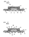
- FIG. 11 of the drawings is shown a schematic representation in cross-section of a representative prior art OMPAC BGA, 110, with an IC unit, 111, being a single die or chip component.
- Device 110 includes a PWB, 112, provided with wirebond fingers, 113, a polymer coating which acts as a solder mask, 114, on the fingers, thruholes, 115, contact pads, 116, wires, 117, interconnecting the die to wirebond fingers 113, and a molding compound, 118, enclosing the die, the wires and those portions of wirebond fingers 113 which are bonded to the wires.
- Contact pads 116 are further provided with solder bumps, 119, for interconnection to a mother board (not shown).
- FIG. 12 of the drawings is shown a schematic representation of another prior art device, 120, a variant of the OMPAC BGA.
- the IC unit is a silicon-on-silicon Multichip Module (MCM) tile, 121, including a plurality of chips or dies, 122 and 123, flip-chip mounted by means of solder or conductive adhesive reflow technology to interconnection circuitry (not shown) on a silicon interconnection substrate, 124.
- Silicon substrate 124 is mounted on a PWB, 125, which is provided with wirebond fingers, 126, a solder mask, 127, plated thruholes, 128, and contact pads, 129.
- the silicon substrate is interconnected by means of wires, 130, to wirebond fingers 126.
- Contact pads 129 are provided with solder bumps, 133, for interconnection to a mother board (not shown).
- device 120 shown in FIG. 12 avoids the molding step, thus avoiding exposure of the assembly to rigors of the molding process.
- device 120 continues the use of wirebond interconnections between the IC unit and the wirebond fingers. Wire bonding is a time-consuming procedure, which becomes more time-consuming as the number of I/O counts per die or MCM tile keeps on increasing.
- the wirebond fingers on the PWB are gold-over-nickel plated copper. By eliminating the wirebond interconnection, the need for expensive gold-over-nickel plating of copper on the PWB would be eliminated. This would lead to a significant cost reduction.
- the MCM tile includes a substrate with a plurality of peripheral metallizations and at least one chip flip-chip mounted on the substrate.
- the PWB is provided with an aperture which is smaller than the size of the substrate but larger than the outside dimensions of the chips.
- the substrate is positioned on the PWB so that its ends overlap areas of the PWB adjacent the aperture and the chips fit into the aperture. Peripheral metallizations on the substrate are interconnected to metallizations on the PWB by solder or conductive adhesive technology.
- FIG. 1 is shown a schematic representation in cross-section of a device, 10, embodying this invention.
- an MCM tile, 11 is mechanically and electrically interconnected to a PWB, 12.
- the latter includes printed circuitry, 13.
- the circuitry is typically copper coated by a polymer mask, 14, except for those areas which are to be used for solder or conductive adhesive interconnection.
- the resist is to prevent spreading of the solder or conductive adhesive beyond the contact area.
- MCM tile 11 is a silicon-on-silicon structure having a silicon substrate, 15, provided with metallizations to which each chip or die, 16 and 17, is interconnected in a flip-chip manner by means of solder, 18.
- solder Alternatively conductive adhesive may be used instead of solder.
- the substrate may be made of other materials including ceramic and plastic materials.
- Peripheral metallizations, 19, are provided on I/O pads of the silicon substrate for interconnecting to circuitry 13 on PWB 12.
- the PWB is provided with a pattern of contact pads which match I/O pads on the silicon substrate of the MCM tile. In order to provide a proper surface for reflow solder, these contact pads are finished with a solder wettable metallization, 23 (FIG.2).
- solder reflow or conductive adhesive interconnection removes the necessity for wire bond connecting the circuitry on the silicon substrate to the circuitry on the PWB.
- the PWB is provided with an aperture, 20.
- the size of aperture 20 is such that, when MCM tile 11 is electrically and mechanically interconnected to PWB 12, chips 16 and 17 on silicon substrate 15 fit into the aperture without contacting the walls of the aperture. Since only the ends of the silicon MCM tile substrate are in contact with circuitry 13 via reflowed solder interconnections, 21, and the chips are within the aperture, the thickness of the assembly is reduced, at least by the thickness of the chips and interconnections between the chips and the silicon substrate. This compares advantageously to the MCM tile-on-PWB assembly thickness that results when the MCM tile is oriented with the chips up and wire bonded to the PWB circuitry 13 as in the prior art e.g. as shown in FIGs. 11 and 12.
- FIG. 2 is shown a schematic diagram for a solder reflow interconnection attachment between silicon substrate 15 of the MCM tile and PWB 12.
- Silicon substrate 15 is provided with peripheral metallizations 19 in the form of metallic contact fingers. Except for an area provided with a solder wettable metallization, 23, which is to be contacted by reflowed solder interconnection 21, each of the contact fingers is coated with polymer 22.
- the PWB includes metallic printed circuitry 13. The latter is also coated with polymer 14 except for a contact area to be contacted with reflowed solder interconnection, 21.
- Polymer 14 functions as a solder mask to prevent the solder from wetting any of the rest of the circuitry beyond the contact area.
- solder wettable base I/O metal pads which are deposited at the same time as the solder wettable metallizations are deposited on the MCM flip-chip pads.
- these solder wettable I/O pads would be configured as 96 ⁇ m by 146 ⁇ m pads on a 305 ⁇ m (12 mil) pitch to facilitate printing with 170 ⁇ m by 280 ⁇ m solder paste deposits at the same time the solder paste is being printed on the internal I/O pads used to attach the chips to the substrate.
- This process may be used with an intermediate to high melting point temperature solder, such as 95/5 Sn/Sb, to produce solder-bumped MCM tiles, that is, MCM tiles on which, after whole wafer assembly, cleaning, testing and separation into individual tiles, each output pad on every tile would be furnished with a solder bump.
- solder-bumped MCM tiles that is, MCM tiles on which, after whole wafer assembly, cleaning, testing and separation into individual tiles, each output pad on every tile would be furnished with a solder bump.
- solder bumps to the MCM tile I/O pads would also improve testability of the MCM tile prior to its assembly with the PWB and hence would increase yields by reducing the number of good tiles that are rejected due to false readings.
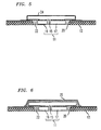
- FIGs. 3 through 9 are shown a few exemplary variants for protecting from the environment the MCM tile and tile-to-PWB interconnections of the assembly shown in FIG. 1.
- the same numerals are being used to denote the same components as are represented in FIGs. 1 and 2. To avoid repetitions not all numerals shown in FIG. 1 are shown in these figures.
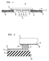
- the cavity formed by silicon substrate 15 and the walls of aperture 20 in the PWB is filled with an encapsulating material, 22, such as silicone gel, which protects the chips, interconnections between the chips and the substrate, interconnections between the substrate and the PWB, and surfaces of the substrate exposed within the cavity.
- an encapsulating material, 22, such as silicone gel which protects the chips, interconnections between the chips and the substrate, interconnections between the substrate and the PWB, and surfaces of the substrate exposed within the cavity.
- FIG. 4 the cavity formed by silicon substrate 15 and the walls of aperture 20 in the PWB is filled, similarly to FIG. 3, with an encapsulating material such as a silicone gel, 22 which protects the chips, interconnections and adjacent surfaces of the substrate. However, other surfaces of the substrate are protected by a compliant "glob top", 23.
- an encapsulating material such as a silicone gel, 22 which protects the chips, interconnections and adjacent surfaces of the substrate.
- other surfaces of the substrate are protected by a compliant "glob top", 23.
- a metallized polymer film, 24, is laminated to the PWB adjacent to silicon substrate 15 and to outer surfaces of the substrate which would otherwise be left exposed. This provides protection without compromising handling the package during testing or assembly, as might a compliant glob top overcoat. It also minimizes the overall package height relative to a package with a glob top.
- the space formed by silicon substrate 15 and the walls of aperture 20 in the PWB is filled with silicon gel 22.
- cup-like cover, 25, is placed over the upper surface of silicon substrate 15 and adhesively secured to the PWB.
- Copper as a metal for the cover is advantageous for its thermal-mechanical properties, for protection against electromagnetic radiation, and for its formability, e.g. by stamping.
- the use of other metals or of a molded plastic cup-like cover is not excluded.
- CTE coefficient of thermal expansion
- Invar® low GTE alloy
- the space over and around the silicon substrate and between the walls of the PWB is also encompassed by highly compliant silicon gel 22.
- Cover 25 is large enough to permit enclosure of the ends of the MCM tile and of the interconnections by the silicone gel.
- FIG. 7 is shown an embodiment in which the cavity is filled by a different compliant encapsulating material, 26, such as an epoxy resin.
- This encapsulating material not only fills the cavity, but is also applied on top of the PWB adjacent the substrate and around the substrate.
- This encapsulating material is acting as a single material substitute for the silicon gel and for a glob top. The extent of coverage by the encapsulating material can be varied as needed.
- the enclosure variants shown in FIGs. 3, 4, 5, 6 and 7 are well suited to rigid printed circuit boards.
- the PWB may be rigid but is so thin that the chips or dies when placed within the aperture in the PWB shall project below the plane of the PWB so that the silicone gel shall not provide sufficient protection to the chips.
- a cup-like metal or plastic cover, 27, is placed on the chip side of the assembly as is shown in FIG. 8. Ends, 28, of the cover are positioned in contact with a thin PWB, 29, and juxtaposed to an area of interconnection between the MCM tile and the PWB providing additional rigidity to the interconnection area.
- the space bounded by cover 27 and silicon substrate 15 is filled with silicone gel 22.
- glob top 23 may be placed over the silicon substrate to further protect the silicon substrate from the environment.
- metallized polymer film similar to film 24 shown in FIG. 5 may be used instead of the glob top.
- encapsulating material 26 may be used instead of silicone gel 22 and placed about the MCM file in the manner shown in FIG. 7.
- FIG. 9 is shown another variant in which a PWB, 30, is not only thin but is also flexible.
- the circuitry on the PWB is interconnected to silicon substrate 15 via solder interconnections, while the chips project through aperture 20 beyond the PWB.
- a cup-like metal or plastic cover, 31, has peripheral edges, 73, which are connected adhesively to and locally support the planar portion of the PWB.
- portions, 33, of the PWB defining aperture 20 are depressed into the cover so that the MCM tile and portions of the PWB are within the cavity formed by the cover.
- the MCM tile, portions 33 of the PWB and interconnections between the MCM tile and the PWB are additionally embedded in silicone gel 22.
- solder bumps, 34 may be provided on PWB 30 for possible interconnection to a mother-board (not shown).
- FIG. 10 is shown a schematic representation of an MCM package 35.
- the MCM package includes a bi-level PWB, 36, having a lower level, 37, and an upper level, 38.
- the PWB is provided with a stepped through-aperture, 39, the size of which is such that, when silicon substrate of the MCM tile is electrically interconnected to the PWB, ends of the silicon substrate overlay regions of the PWB adjacent to the aperture in the lower level 37 of the PWB while chips on the silicon substrate face downward and fit into the aperture in the lower level without contacting the walls of the aperture.
- MCM tile 11 is positioned such that free surface of silicon substrate 15 of the MCM tile faces upwardly while chips 16 and 17 face downwardly through the aperture in the lower level and, yet, the chips are recessed within the aperture relative to the bottom surface of the lower level of the PWB.
- Bond fingers 19 on the silicon substrate are electrically connected to contacts, 13, on the PWB, by means of solder interconnections, 21.
- MCM tile is encapsulated with silicon gel 22 protectively enclosing interconnections between the chips and the silicon substrate and between the bond fingers on the silicon substrate and the contacts on the PWB.
- the thickness of the assembly is reduced to the thickness of the PWB. This compares favorably to the MCM tile-on-PWB assembly thickness that results with the MCM tile mounted on top of the PWB, oriented with the chips up, and wire bonded to the PWB circuitry as in the prior art exemplified by FIGs. 11 and 12.
- the PWB is to be an intermediate interconnection or a leadframe board which is mounted to a mother-board (either a single-sided flexible PWB or a double-sided rigid PWB with plated thruholes)
- its metallizations should be patterned so as to mate with the mother-board through an I/O array of robustly solder printable bumped solder pads, such as bumps 34. Bumped solder pads are advantageous but pads without solder bumps are not excluded from this invention.
Landscapes
- Engineering & Computer Science (AREA)
- Manufacturing & Machinery (AREA)
- Microelectronics & Electronic Packaging (AREA)
- Wire Bonding (AREA)
- Structures Or Materials For Encapsulating Or Coating Semiconductor Devices Or Solid State Devices (AREA)
- Structures For Mounting Electric Components On Printed Circuit Boards (AREA)
Applications Claiming Priority (2)
| Application Number | Priority Date | Filing Date | Title |
|---|---|---|---|
| US08/393,628 US5608262A (en) | 1995-02-24 | 1995-02-24 | Packaging multi-chip modules without wire-bond interconnection |
| US393628 | 1995-02-24 |
Publications (3)
| Publication Number | Publication Date |
|---|---|
| EP0729180A2 true EP0729180A2 (fr) | 1996-08-28 |
| EP0729180A3 EP0729180A3 (fr) | 1998-11-11 |
| EP0729180B1 EP0729180B1 (fr) | 2003-04-23 |
Family
ID=23555559
Family Applications (1)
| Application Number | Title | Priority Date | Filing Date |
|---|---|---|---|
| EP96301025A Expired - Lifetime EP0729180B1 (fr) | 1995-02-24 | 1996-02-14 | Empaquetage de modules à multi-puces sans interconnexion à fil |
Country Status (8)
| Country | Link |
|---|---|
| US (1) | US5608262A (fr) |
| EP (1) | EP0729180B1 (fr) |
| JP (1) | JP3209320B2 (fr) |
| KR (1) | KR100380950B1 (fr) |
| CA (1) | CA2166926C (fr) |
| DE (1) | DE69627565T2 (fr) |
| SG (1) | SG38976A1 (fr) |
| TW (1) | TW376574B (fr) |
Cited By (7)
| Publication number | Priority date | Publication date | Assignee | Title |
|---|---|---|---|---|
| WO1999019911A1 (fr) * | 1997-10-10 | 1999-04-22 | Gennum Corporation | Configuration tridimensionnelle de mise sous boitier pour ensemble de module multipuce |
| EP0880175A3 (fr) * | 1997-04-21 | 1999-05-12 | Lsi Logic Corporation | Boítier de puissance mince de type grille de boule à bande |
| WO2000004595A3 (fr) * | 1998-07-20 | 2000-06-29 | Intel Corp | Montage sur face plage de composants sur un boitier de microcircuit |
| EP0959500A3 (fr) * | 1998-05-19 | 2004-09-29 | Lucent Technologies Inc. | Empaquetage de modules à multi-puces de type silicium-sur-silicium |
| WO2010036496A1 (fr) * | 2008-09-26 | 2010-04-01 | Siemens Energy, Inc. | Carte de circuits imprimés pour environnements difficiles |
| CN103379736A (zh) * | 2012-04-13 | 2013-10-30 | 广达电脑股份有限公司 | 系统级封装组件、印刷电路板组件及其制作方法 |
| CN110581104A (zh) * | 2018-06-11 | 2019-12-17 | 奥特斯奥地利科技与系统技术有限公司 | 容置在部件承载件中的阶梯式腔内的阶梯式部件组件 |
Families Citing this family (202)
| Publication number | Priority date | Publication date | Assignee | Title |
|---|---|---|---|---|
| FR2728392A1 (fr) * | 1994-12-16 | 1996-06-21 | Bull Sa | Procede et support de connexion d'un circuit integre a un autre support par l'intermediaire de boules |
| JP3014029B2 (ja) * | 1995-06-16 | 2000-02-28 | 日本電気株式会社 | 半導体素子の実装方法 |
| JPH0964244A (ja) * | 1995-08-17 | 1997-03-07 | Hitachi Ltd | 半導体装置およびその製造方法 |
| JP3332308B2 (ja) * | 1995-11-07 | 2002-10-07 | 新光電気工業株式会社 | 半導体装置及びその製造方法 |
| JP3527350B2 (ja) * | 1996-02-01 | 2004-05-17 | 株式会社ルネサステクノロジ | 半導体装置 |
| US6682954B1 (en) | 1996-05-29 | 2004-01-27 | Micron Technology, Inc. | Method for employing piggyback multiple die #3 |
| JPH1032221A (ja) * | 1996-07-12 | 1998-02-03 | Nec Corp | プリント配線基板 |
| US6075711A (en) * | 1996-10-21 | 2000-06-13 | Alpine Microsystems, Inc. | System and method for routing connections of integrated circuits |
| US5815372A (en) * | 1997-03-25 | 1998-09-29 | Intel Corporation | Packaging multiple dies on a ball grid array substrate |
| US5889654A (en) * | 1997-04-09 | 1999-03-30 | International Business Machines Corporation | Advanced chip packaging structure for memory card applications |
| EP1004141A4 (fr) * | 1997-05-23 | 2001-01-24 | Alpine Microsystems Inc | Systeme et procede d'encapsulation de circuits integres |
| US6208018B1 (en) * | 1997-05-29 | 2001-03-27 | Micron Technology, Inc. | Piggyback multiple dice assembly |
| US5790384A (en) * | 1997-06-26 | 1998-08-04 | International Business Machines Corporation | Bare die multiple dies for direct attach |
| US5869894A (en) * | 1997-07-18 | 1999-02-09 | Lucent Technologies Inc. | RF IC package |
| US5963429A (en) * | 1997-08-20 | 1999-10-05 | Sulzer Intermedics Inc. | Printed circuit substrate with cavities for encapsulating integrated circuits |
| US5798567A (en) * | 1997-08-21 | 1998-08-25 | Hewlett-Packard Company | Ball grid array integrated circuit package which employs a flip chip integrated circuit and decoupling capacitors |
| US6441487B2 (en) | 1997-10-20 | 2002-08-27 | Flip Chip Technologies, L.L.C. | Chip scale package using large ductile solder balls |
| US6117382A (en) | 1998-02-05 | 2000-09-12 | Micron Technology, Inc. | Method for encasing array packages |
| US5977640A (en) * | 1998-06-26 | 1999-11-02 | International Business Machines Corporation | Highly integrated chip-on-chip packaging |
| US6084308A (en) * | 1998-06-30 | 2000-07-04 | National Semiconductor Corporation | Chip-on-chip integrated circuit package and method for making the same |
| US6154370A (en) * | 1998-07-21 | 2000-11-28 | Lucent Technologies Inc. | Recessed flip-chip package |
| US6160715A (en) * | 1998-09-08 | 2000-12-12 | Lucent Technologies Inc. | Translator for recessed flip-chip package |
| US6175158B1 (en) * | 1998-09-08 | 2001-01-16 | Lucent Technologies Inc. | Interposer for recessed flip-chip package |
| US6154371A (en) * | 1998-09-30 | 2000-11-28 | Cisco Technology, Inc. | Printed circuit board assembly and method |
| US6329713B1 (en) * | 1998-10-21 | 2001-12-11 | International Business Machines Corporation | Integrated circuit chip carrier assembly comprising a stiffener attached to a dielectric substrate |
| US6184465B1 (en) | 1998-11-12 | 2001-02-06 | Micron Technology, Inc. | Semiconductor package |
| US6303423B1 (en) | 1998-12-21 | 2001-10-16 | Megic Corporation | Method for forming high performance system-on-chip using post passivation process |
| US6869870B2 (en) * | 1998-12-21 | 2005-03-22 | Megic Corporation | High performance system-on-chip discrete components using post passivation process |
| US8178435B2 (en) | 1998-12-21 | 2012-05-15 | Megica Corporation | High performance system-on-chip inductor using post passivation process |
| US8421158B2 (en) * | 1998-12-21 | 2013-04-16 | Megica Corporation | Chip structure with a passive device and method for forming the same |
| US6965165B2 (en) * | 1998-12-21 | 2005-11-15 | Mou-Shiung Lin | Top layers of metal for high performance IC's |
| US7531417B2 (en) * | 1998-12-21 | 2009-05-12 | Megica Corporation | High performance system-on-chip passive device using post passivation process |
| JP2000223657A (ja) * | 1999-02-03 | 2000-08-11 | Rohm Co Ltd | 半導体装置およびそれに用いる半導体チップ |
| JP2000252414A (ja) * | 1999-03-04 | 2000-09-14 | Mitsubishi Electric Corp | 半導体装置 |
| US6268660B1 (en) * | 1999-03-05 | 2001-07-31 | International Business Machines Corporation | Silicon packaging with through wafer interconnects |
| US6215193B1 (en) * | 1999-04-21 | 2001-04-10 | Advanced Semiconductor Engineering, Inc. | Multichip modules and manufacturing method therefor |
| US6498708B2 (en) * | 1999-05-27 | 2002-12-24 | Emerson Electric Co. | Method and apparatus for mounting printed circuit board components |
| KR100393095B1 (ko) * | 1999-06-12 | 2003-07-31 | 앰코 테크놀로지 코리아 주식회사 | 반도체패키지와 그 제조방법 |
| US6049275A (en) * | 1999-06-15 | 2000-04-11 | Hou; Chien Tzu | Security mechanism for an IC packing box |
| US6335566B1 (en) * | 1999-06-17 | 2002-01-01 | Hitachi, Ltd. | Semiconductor device and an electronic device |
| US6232667B1 (en) | 1999-06-29 | 2001-05-15 | International Business Machines Corporation | Technique for underfilling stacked chips on a cavity MLC module |
| US6297551B1 (en) * | 1999-09-22 | 2001-10-02 | Agere Systems Guardian Corp. | Integrated circuit packages with improved EMI characteristics |
| US6559531B1 (en) | 1999-10-14 | 2003-05-06 | Sun Microsystems, Inc. | Face to face chips |
| US6483101B1 (en) * | 1999-12-08 | 2002-11-19 | Amkor Technology, Inc. | Molded image sensor package having lens holder |
| US6369448B1 (en) | 2000-01-21 | 2002-04-09 | Lsi Logic Corporation | Vertically integrated flip chip semiconductor package |
| US6414396B1 (en) * | 2000-01-24 | 2002-07-02 | Amkor Technology, Inc. | Package for stacked integrated circuits |
| JP3996315B2 (ja) * | 2000-02-21 | 2007-10-24 | 松下電器産業株式会社 | 半導体装置およびその製造方法 |
| JP3417380B2 (ja) | 2000-04-05 | 2003-06-16 | 株式会社村田製作所 | 非可逆回路素子および通信装置 |
| US6916121B2 (en) * | 2001-08-03 | 2005-07-12 | National Semiconductor Corporation | Optical sub-assembly for optoelectronic modules |
| US6765275B1 (en) * | 2000-05-09 | 2004-07-20 | National Semiconductor Corporation | Two-layer electrical substrate for optical devices |
| US6707140B1 (en) | 2000-05-09 | 2004-03-16 | National Semiconductor Corporation | Arrayable, scaleable, and stackable molded package configuration |
| US6624507B1 (en) | 2000-05-09 | 2003-09-23 | National Semiconductor Corporation | Miniature semiconductor package for opto-electronic devices |
| US6642613B1 (en) * | 2000-05-09 | 2003-11-04 | National Semiconductor Corporation | Techniques for joining an opto-electronic module to a semiconductor package |
| US6767140B2 (en) * | 2000-05-09 | 2004-07-27 | National Semiconductor Corporation | Ceramic optical sub-assembly for opto-electronic module utilizing LTCC (low-temperature co-fired ceramic) technology |
| US7247932B1 (en) * | 2000-05-19 | 2007-07-24 | Megica Corporation | Chip package with capacitor |
| US6356453B1 (en) * | 2000-06-29 | 2002-03-12 | Amkor Technology, Inc. | Electronic package having flip chip integrated circuit and passive chip component |
| US6546620B1 (en) | 2000-06-29 | 2003-04-15 | Amkor Technology, Inc. | Flip chip integrated circuit and passive chip component package fabrication method |
| JP3829050B2 (ja) * | 2000-08-29 | 2006-10-04 | 松下電器産業株式会社 | 一体型電子部品 |
| TW569403B (en) * | 2001-04-12 | 2004-01-01 | Siliconware Precision Industries Co Ltd | Multi-chip module and its manufacturing method |
| JP4497683B2 (ja) * | 2000-09-11 | 2010-07-07 | ローム株式会社 | 集積回路装置 |
| KR100508261B1 (ko) * | 2000-10-04 | 2005-08-18 | 앰코 테크놀로지 코리아 주식회사 | 반도체 패키지 및 그 제조방법 |
| JP4505983B2 (ja) * | 2000-12-01 | 2010-07-21 | 日本電気株式会社 | 半導体装置 |
| KR100705248B1 (ko) * | 2000-12-04 | 2007-04-06 | 앰코 테크놀로지 코리아 주식회사 | 반도체 패키지 및 그 제조방법 |
| KR20020058201A (ko) * | 2000-12-29 | 2002-07-12 | 마이클 디. 오브라이언 | 반도체패키지 및 그 제조 방법 |
| US6888240B2 (en) * | 2001-04-30 | 2005-05-03 | Intel Corporation | High performance, low cost microelectronic circuit package with interposer |
| US6894399B2 (en) | 2001-04-30 | 2005-05-17 | Intel Corporation | Microelectronic device having signal distribution functionality on an interfacial layer thereof |
| US6610560B2 (en) | 2001-05-11 | 2003-08-26 | Siliconware Precision Industries Co., Ltd. | Chip-on-chip based multi-chip module with molded underfill and method of fabricating the same |
| US20020167804A1 (en) * | 2001-05-14 | 2002-11-14 | Intel Corporation | Polymeric encapsulation material with fibrous filler for use in microelectronic circuit packaging |
| US7071024B2 (en) * | 2001-05-21 | 2006-07-04 | Intel Corporation | Method for packaging a microelectronic device using on-die bond pad expansion |
| US6730536B1 (en) | 2001-06-28 | 2004-05-04 | Amkor Technology, Inc. | Pre-drilled image sensor package fabrication method |
| US6548759B1 (en) | 2001-06-28 | 2003-04-15 | Amkor Technology, Inc. | Pre-drilled image sensor package |
| US6486545B1 (en) * | 2001-07-26 | 2002-11-26 | Amkor Technology, Inc. | Pre-drilled ball grid array package |
| US7269027B2 (en) * | 2001-08-03 | 2007-09-11 | National Semiconductor Corporation | Ceramic optical sub-assembly for optoelectronic modules |
| US7023705B2 (en) | 2001-08-03 | 2006-04-04 | National Semiconductor Corporation | Ceramic optical sub-assembly for optoelectronic modules |
| US7176506B2 (en) * | 2001-08-28 | 2007-02-13 | Tessera, Inc. | High frequency chip packages with connecting elements |
| US6856007B2 (en) * | 2001-08-28 | 2005-02-15 | Tessera, Inc. | High-frequency chip packages |
| DE10142655A1 (de) * | 2001-08-31 | 2003-04-03 | Epcos Ag | Bauelementanordnung |
| US6759275B1 (en) * | 2001-09-04 | 2004-07-06 | Megic Corporation | Method for making high-performance RF integrated circuits |
| US7183658B2 (en) | 2001-09-05 | 2007-02-27 | Intel Corporation | Low cost microelectronic circuit package |
| US20030057544A1 (en) * | 2001-09-13 | 2003-03-27 | Nathan Richard J. | Integrated assembly protocol |
| US6613606B1 (en) * | 2001-09-17 | 2003-09-02 | Magic Corporation | Structure of high performance combo chip and processing method |
| US6847105B2 (en) | 2001-09-21 | 2005-01-25 | Micron Technology, Inc. | Bumping technology in stacked die configurations |
| US20030059976A1 (en) * | 2001-09-24 | 2003-03-27 | Nathan Richard J. | Integrated package and methods for making same |
| US6973225B2 (en) * | 2001-09-24 | 2005-12-06 | National Semiconductor Corporation | Techniques for attaching rotated photonic devices to an optical sub-assembly in an optoelectronic package |
| US7134486B2 (en) * | 2001-09-28 | 2006-11-14 | The Board Of Trustees Of The Leeland Stanford Junior University | Control of electrolysis gases in electroosmotic pump systems |
| US6942018B2 (en) | 2001-09-28 | 2005-09-13 | The Board Of Trustees Of The Leland Stanford Junior University | Electroosmotic microchannel cooling system |
| GB0128351D0 (en) * | 2001-11-27 | 2002-01-16 | Koninkl Philips Electronics Nv | Multi-chip module semiconductor devices |
| US6606251B1 (en) | 2002-02-07 | 2003-08-12 | Cooligy Inc. | Power conditioning module |
| US20030153119A1 (en) * | 2002-02-14 | 2003-08-14 | Nathan Richard J. | Integrated circuit package and method for fabrication |
| US6767765B2 (en) * | 2002-03-27 | 2004-07-27 | Intel Corporation | Methods and apparatus for disposing a thermal interface material between a heat source and a heat dissipation device |
| US20030183934A1 (en) * | 2002-03-29 | 2003-10-02 | Barrett Joseph C. | Method and apparatus for stacking multiple die in a flip chip semiconductor package |
| US6903458B1 (en) * | 2002-06-20 | 2005-06-07 | Richard J. Nathan | Embedded carrier for an integrated circuit chip |
| JP4601892B2 (ja) * | 2002-07-04 | 2010-12-22 | ラムバス・インコーポレーテッド | 半導体装置および半導体チップのバンプ製造方法 |
| US6885107B2 (en) * | 2002-08-29 | 2005-04-26 | Micron Technology, Inc. | Flip-chip image sensor packages and methods of fabrication |
| US6879040B2 (en) * | 2002-09-18 | 2005-04-12 | Agilent Technologies, Inc. | Surface mountable electronic device |
| US7400036B2 (en) * | 2002-12-16 | 2008-07-15 | Avago Technologies General Ip Pte Ltd | Semiconductor chip package with a package substrate and a lid cover |
| US6833628B2 (en) * | 2002-12-17 | 2004-12-21 | Delphi Technologies, Inc. | Mutli-chip module |
| JP4110992B2 (ja) * | 2003-02-07 | 2008-07-02 | セイコーエプソン株式会社 | 半導体装置、電子デバイス、電子機器、半導体装置の製造方法および電子デバイスの製造方法 |
| US7754537B2 (en) * | 2003-02-25 | 2010-07-13 | Tessera, Inc. | Manufacture of mountable capped chips |
| US20040217471A1 (en) * | 2003-02-27 | 2004-11-04 | Tessera, Inc. | Component and assemblies with ends offset downwardly |
| US8368150B2 (en) * | 2003-03-17 | 2013-02-05 | Megica Corporation | High performance IC chip having discrete decoupling capacitors attached to its IC surface |
| TWI230447B (en) * | 2003-04-25 | 2005-04-01 | Advanced Semiconductor Eng | Multi-chips package |
| TWI236763B (en) * | 2003-05-27 | 2005-07-21 | Megic Corp | High performance system-on-chip inductor using post passivation process |
| US6972480B2 (en) | 2003-06-16 | 2005-12-06 | Shellcase Ltd. | Methods and apparatus for packaging integrated circuit devices |
| WO2005004195A2 (fr) * | 2003-07-03 | 2005-01-13 | Shellcase Ltd. | Procede et appareil d'encapsulation de circuits integres |
| US6873040B2 (en) * | 2003-07-08 | 2005-03-29 | Texas Instruments Incorporated | Semiconductor packages for enhanced number of terminals, speed and power performance |
| US7156562B2 (en) * | 2003-07-15 | 2007-01-02 | National Semiconductor Corporation | Opto-electronic module form factor having adjustable optical plane height |
| US6985668B2 (en) * | 2003-07-15 | 2006-01-10 | National Semiconductor Corporation | Multi-purpose optical light pipe |
| WO2005022591A2 (fr) * | 2003-08-26 | 2005-03-10 | Advanced Interconnect Technologies Limited | Boitier a souder reversible, son procede de production et son utilisation |
| US7224056B2 (en) * | 2003-09-26 | 2007-05-29 | Tessera, Inc. | Back-face and edge interconnects for lidded package |
| US20050067681A1 (en) * | 2003-09-26 | 2005-03-31 | Tessera, Inc. | Package having integral lens and wafer-scale fabrication method therefor |
| US20050093175A1 (en) * | 2003-11-03 | 2005-05-05 | Martin Reiss | Arrangement for improving the reliability of semiconductor modules |
| US20050139984A1 (en) * | 2003-12-19 | 2005-06-30 | Tessera, Inc. | Package element and packaged chip having severable electrically conductive ties |
| US7521785B2 (en) * | 2003-12-23 | 2009-04-21 | Tessera, Inc. | Packaged systems with MRAM |
| TWI233170B (en) * | 2004-02-05 | 2005-05-21 | United Microelectronics Corp | Ultra-thin wafer level stack packaging method and structure using thereof |
| WO2005086532A2 (fr) * | 2004-03-01 | 2005-09-15 | Tessera, Inc. | Puces a transducteur acoustique et electromagnetique encapsulees |
| US8008775B2 (en) | 2004-09-09 | 2011-08-30 | Megica Corporation | Post passivation interconnection structures |
| US7355282B2 (en) * | 2004-09-09 | 2008-04-08 | Megica Corporation | Post passivation interconnection process and structures |
| JP4146826B2 (ja) * | 2004-09-14 | 2008-09-10 | カシオマイクロニクス株式会社 | 配線基板及び半導体装置 |
| TWI393228B (zh) * | 2004-12-14 | 2013-04-11 | 飛思卡爾半導體公司 | 覆晶及焊線封裝半導體 |
| JP4581768B2 (ja) * | 2005-03-16 | 2010-11-17 | ソニー株式会社 | 半導体装置の製造方法 |
| US8143095B2 (en) * | 2005-03-22 | 2012-03-27 | Tessera, Inc. | Sequential fabrication of vertical conductive interconnects in capped chips |
| US8384189B2 (en) * | 2005-03-29 | 2013-02-26 | Megica Corporation | High performance system-on-chip using post passivation process |
| US8130560B1 (en) | 2006-11-13 | 2012-03-06 | Google Inc. | Multi-rank partial width memory modules |
| US7386656B2 (en) | 2006-07-31 | 2008-06-10 | Metaram, Inc. | Interface circuit system and method for performing power management operations in conjunction with only a portion of a memory circuit |
| US8359187B2 (en) | 2005-06-24 | 2013-01-22 | Google Inc. | Simulating a different number of memory circuit devices |
| US8055833B2 (en) | 2006-10-05 | 2011-11-08 | Google Inc. | System and method for increasing capacity, performance, and flexibility of flash storage |
| US10013371B2 (en) | 2005-06-24 | 2018-07-03 | Google Llc | Configurable memory circuit system and method |
| GB2441726B (en) * | 2005-06-24 | 2010-08-11 | Metaram Inc | An integrated memory core and memory interface circuit |
| US8090897B2 (en) | 2006-07-31 | 2012-01-03 | Google Inc. | System and method for simulating an aspect of a memory circuit |
| US8386722B1 (en) | 2008-06-23 | 2013-02-26 | Google Inc. | Stacked DIMM memory interface |
| US9171585B2 (en) | 2005-06-24 | 2015-10-27 | Google Inc. | Configurable memory circuit system and method |
| US20080082763A1 (en) | 2006-10-02 | 2008-04-03 | Metaram, Inc. | Apparatus and method for power management of memory circuits by a system or component thereof |
| US8089795B2 (en) | 2006-02-09 | 2012-01-03 | Google Inc. | Memory module with memory stack and interface with enhanced capabilities |
| US8111566B1 (en) | 2007-11-16 | 2012-02-07 | Google, Inc. | Optimal channel design for memory devices for providing a high-speed memory interface |
| US8081474B1 (en) | 2007-12-18 | 2011-12-20 | Google Inc. | Embossed heat spreader |
| US20080028136A1 (en) * | 2006-07-31 | 2008-01-31 | Schakel Keith R | Method and apparatus for refresh management of memory modules |
| US8077535B2 (en) | 2006-07-31 | 2011-12-13 | Google Inc. | Memory refresh apparatus and method |
| US9542352B2 (en) * | 2006-02-09 | 2017-01-10 | Google Inc. | System and method for reducing command scheduling constraints of memory circuits |
| US8060774B2 (en) | 2005-06-24 | 2011-11-15 | Google Inc. | Memory systems and memory modules |
| US9507739B2 (en) | 2005-06-24 | 2016-11-29 | Google Inc. | Configurable memory circuit system and method |
| US8335894B1 (en) | 2008-07-25 | 2012-12-18 | Google Inc. | Configurable memory system with interface circuit |
| US8327104B2 (en) | 2006-07-31 | 2012-12-04 | Google Inc. | Adjusting the timing of signals associated with a memory system |
| US8244971B2 (en) | 2006-07-31 | 2012-08-14 | Google Inc. | Memory circuit system and method |
| US8796830B1 (en) | 2006-09-01 | 2014-08-05 | Google Inc. | Stackable low-profile lead frame package |
| US7609567B2 (en) * | 2005-06-24 | 2009-10-27 | Metaram, Inc. | System and method for simulating an aspect of a memory circuit |
| US8438328B2 (en) | 2008-02-21 | 2013-05-07 | Google Inc. | Emulation of abstracted DIMMs using abstracted DRAMs |
| US8041881B2 (en) | 2006-07-31 | 2011-10-18 | Google Inc. | Memory device with emulated characteristics |
| US8397013B1 (en) | 2006-10-05 | 2013-03-12 | Google Inc. | Hybrid memory module |
| CN1901162B (zh) * | 2005-07-22 | 2011-04-20 | 米辑电子股份有限公司 | 连续电镀制作线路组件的方法及线路组件结构 |
| JP5242397B2 (ja) | 2005-09-02 | 2013-07-24 | メタラム インコーポレイテッド | Dramをスタックする方法及び装置 |
| CN100561725C (zh) * | 2005-11-25 | 2009-11-18 | 全懋精密科技股份有限公司 | 半导体芯片的直接电性连接倒装芯片封装结构 |
| US7943431B2 (en) * | 2005-12-02 | 2011-05-17 | Unisem (Mauritius) Holdings Limited | Leadless semiconductor package and method of manufacture |
| US7402442B2 (en) * | 2005-12-21 | 2008-07-22 | International Business Machines Corporation | Physically highly secure multi-chip assembly |
| US7304382B2 (en) * | 2006-01-11 | 2007-12-04 | Staktek Group L.P. | Managed memory component |
| US20070190747A1 (en) * | 2006-01-23 | 2007-08-16 | Tessera Technologies Hungary Kft. | Wafer level packaging to lidded chips |
| US7936062B2 (en) * | 2006-01-23 | 2011-05-03 | Tessera Technologies Ireland Limited | Wafer level chip packaging |
| US9632929B2 (en) | 2006-02-09 | 2017-04-25 | Google Inc. | Translating an address associated with a command communicated between a system and memory circuits |
| US20080002460A1 (en) * | 2006-03-01 | 2008-01-03 | Tessera, Inc. | Structure and method of making lidded chips |
| US7663232B2 (en) * | 2006-03-07 | 2010-02-16 | Micron Technology, Inc. | Elongated fasteners for securing together electronic components and substrates, semiconductor device assemblies including such fasteners, and accompanying systems |
| US7304859B2 (en) * | 2006-03-30 | 2007-12-04 | Stats Chippac Ltd. | Chip carrier and fabrication method |
| US7724589B2 (en) | 2006-07-31 | 2010-05-25 | Google Inc. | System and method for delaying a signal communicated from a system to at least one of a plurality of memory circuits |
| JP2008042077A (ja) * | 2006-08-09 | 2008-02-21 | Renesas Technology Corp | 半導体装置及びその製造方法 |
| US20080123318A1 (en) * | 2006-11-08 | 2008-05-29 | Atmel Corporation | Multi-component electronic package with planarized embedded-components substrate |
| CN101211882B (zh) * | 2006-12-31 | 2010-12-08 | 北京华旗资讯数码科技有限公司 | 印刷电路板与元件模块的封装结构及封装方法 |
| US7863189B2 (en) * | 2007-01-05 | 2011-01-04 | International Business Machines Corporation | Methods for fabricating silicon carriers with conductive through-vias with low stress and low defect density |
| US8604605B2 (en) | 2007-01-05 | 2013-12-10 | Invensas Corp. | Microelectronic assembly with multi-layer support structure |
| US7965520B2 (en) * | 2007-01-22 | 2011-06-21 | Sony Ericsson Mobile Communications Ab | Electronic device with flip module having low height |
| DE102007006462A1 (de) * | 2007-02-05 | 2008-08-14 | Siemens Ag | Elektronische Schaltungsanordnung mit einer ersten und zweiten Leiterplatte |
| US9466545B1 (en) * | 2007-02-21 | 2016-10-11 | Amkor Technology, Inc. | Semiconductor package in package |
| US20080284037A1 (en) | 2007-05-15 | 2008-11-20 | Andry Paul S | Apparatus and Methods for Constructing Semiconductor Chip Packages with Silicon Space Transformer Carriers |
| US8209479B2 (en) | 2007-07-18 | 2012-06-26 | Google Inc. | Memory circuit system and method |
| US8080874B1 (en) | 2007-09-14 | 2011-12-20 | Google Inc. | Providing additional space between an integrated circuit and a circuit board for positioning a component therebetween |
| US7915724B2 (en) * | 2007-09-28 | 2011-03-29 | Stats Chippac Ltd. | Integrated circuit packaging system with base structure device |
| US8258614B2 (en) * | 2007-11-12 | 2012-09-04 | Stats Chippac Ltd. | Integrated circuit package system with package integration |
| JP2009302212A (ja) | 2008-06-11 | 2009-12-24 | Fujitsu Microelectronics Ltd | 半導体装置及びその製造方法 |
| US8836115B1 (en) | 2008-07-31 | 2014-09-16 | Amkor Technology, Inc. | Stacked inverted flip chip package and fabrication method |
| US20100244276A1 (en) * | 2009-03-25 | 2010-09-30 | Lsi Corporation | Three-dimensional electronics package |
| US8804368B2 (en) * | 2009-04-30 | 2014-08-12 | Sony Corporation | Downward-facing optical component module |
| WO2010144624A1 (fr) | 2009-06-09 | 2010-12-16 | Google Inc. | Programmation de valeurs de résistance de terminaison dimm |
| US8227904B2 (en) | 2009-06-24 | 2012-07-24 | Intel Corporation | Multi-chip package and method of providing die-to-die interconnects in same |
| CN102130098B (zh) | 2010-01-20 | 2015-11-25 | 飞思卡尔半导体公司 | 双管芯半导体封装 |
| US8278756B2 (en) * | 2010-02-24 | 2012-10-02 | Inpaq Technology Co., Ltd. | Single chip semiconductor coating structure and manufacturing method thereof |
| US8590387B2 (en) * | 2011-03-31 | 2013-11-26 | DePuy Synthes Products, LLC | Absolute capacitive micro pressure sensor |
| KR101387208B1 (ko) * | 2012-06-04 | 2014-04-29 | 삼성전기주식회사 | 임베디드 기판 제조방법 및 임베디드 기판 |
| EP2811427A1 (fr) * | 2013-06-07 | 2014-12-10 | Gemalto SA | Procédé de fabrication d'un dispositif électronique anti-fissuration |
| KR20150025129A (ko) * | 2013-08-28 | 2015-03-10 | 삼성전기주식회사 | 전자 소자 모듈 및 그 제조 방법 |
| US20150255411A1 (en) * | 2014-03-05 | 2015-09-10 | Omkar G. Karhade | Die-to-die bonding and associated package configurations |
| US10141201B2 (en) * | 2014-06-13 | 2018-11-27 | Taiwan Semiconductor Manufacturing Company | Integrated circuit packages and methods of forming same |
| US20150380392A1 (en) * | 2014-06-27 | 2015-12-31 | Apple Inc. | Package with memory die and logic die interconnected in a face-to-face configuration |
| CN106960799B (zh) * | 2016-01-12 | 2022-11-22 | 恩智浦美国有限公司 | 集成电路装置及其三维扇出结构和制造方法 |
| US11862983B1 (en) | 2019-03-28 | 2024-01-02 | Roger W. Graham | Earth energy systems and devices |
| US11270946B2 (en) * | 2019-08-30 | 2022-03-08 | Stmicroelectronics Pte Ltd | Package with electrical interconnection bridge |
| JP7268544B2 (ja) * | 2019-08-30 | 2023-05-08 | 富士通株式会社 | 電気チップ及び光モジュール |
| CN110759311A (zh) * | 2019-10-29 | 2020-02-07 | 太极半导体(苏州)有限公司 | 一种基于窗口式基板的无引线mems芯片封装结构及其工艺 |
| KR102822947B1 (ko) * | 2020-06-29 | 2025-06-20 | 삼성전자주식회사 | 반도체 패키지, 및 이를 가지는 패키지 온 패키지 |
| US12355000B2 (en) * | 2020-11-10 | 2025-07-08 | Qualcomm Incorporated | Package comprising a substrate and a high-density interconnect integrated device |
| AU2021393225B2 (en) * | 2020-12-02 | 2024-11-21 | Miwa Kankyo Co., Ltd. | Oxygen-hydrogen mixed gas generation device |
| US12469811B2 (en) | 2021-03-26 | 2025-11-11 | Qualcomm Incorporated | Package comprising wire bonds coupled to integrated devices |
| US12002795B2 (en) | 2022-04-13 | 2024-06-04 | Google Llc | Pluggable CPU modules with vertical power |
| US12308543B2 (en) | 2022-04-18 | 2025-05-20 | Google Llc | Structure for optimal XPU socket compression |
| CN115444426B (zh) * | 2022-11-09 | 2023-04-28 | 之江实验室 | 片上电极集成的无线肌电SoC系统、芯片及采集装置 |
Family Cites Families (6)
| Publication number | Priority date | Publication date | Assignee | Title |
|---|---|---|---|---|
| GB2098398A (en) * | 1981-05-13 | 1982-11-17 | Honeywell Ltd | Electronic packaging system |
| FR2535110B1 (fr) * | 1982-10-20 | 1986-07-25 | Radiotechnique Compelec | Procede d'encapsulation d'un composant semi-conducteur dans un circuit electronique realise sur substrat et application aux circuits integres rapides |
| US4903120A (en) * | 1985-11-22 | 1990-02-20 | Texas Instruments Incorporated | Chip carrier with interconnects on lid |
| US4843188A (en) * | 1986-03-25 | 1989-06-27 | Western Digital Corporation | Integrated circuit chip mounting and packaging assembly |
| US5138436A (en) * | 1990-11-16 | 1992-08-11 | Ball Corporation | Interconnect package having means for waveguide transmission of rf signals |
| JPH0513659A (ja) * | 1991-07-03 | 1993-01-22 | Hitachi Ltd | 半導体集積回路装置の製造方法 |
-
1995
- 1995-02-24 US US08/393,628 patent/US5608262A/en not_active Expired - Lifetime
- 1995-10-24 TW TW084111255A patent/TW376574B/zh not_active IP Right Cessation
-
1996
- 1996-01-10 CA CA002166926A patent/CA2166926C/fr not_active Expired - Fee Related
- 1996-02-13 SG SG1996011079A patent/SG38976A1/en unknown
- 1996-02-14 EP EP96301025A patent/EP0729180B1/fr not_active Expired - Lifetime
- 1996-02-14 DE DE69627565T patent/DE69627565T2/de not_active Expired - Lifetime
- 1996-02-23 JP JP03610496A patent/JP3209320B2/ja not_active Expired - Lifetime
- 1996-02-23 KR KR1019960004374A patent/KR100380950B1/ko not_active Expired - Lifetime
Cited By (12)
| Publication number | Priority date | Publication date | Assignee | Title |
|---|---|---|---|---|
| EP0880175A3 (fr) * | 1997-04-21 | 1999-05-12 | Lsi Logic Corporation | Boítier de puissance mince de type grille de boule à bande |
| WO1999019911A1 (fr) * | 1997-10-10 | 1999-04-22 | Gennum Corporation | Configuration tridimensionnelle de mise sous boitier pour ensemble de module multipuce |
| US6133626A (en) * | 1997-10-10 | 2000-10-17 | Gennum Corporation | Three dimensional packaging configuration for multi-chip module assembly |
| EP0959500A3 (fr) * | 1998-05-19 | 2004-09-29 | Lucent Technologies Inc. | Empaquetage de modules à multi-puces de type silicium-sur-silicium |
| WO2000004595A3 (fr) * | 1998-07-20 | 2000-06-29 | Intel Corp | Montage sur face plage de composants sur un boitier de microcircuit |
| WO2010036496A1 (fr) * | 2008-09-26 | 2010-04-01 | Siemens Energy, Inc. | Carte de circuits imprimés pour environnements difficiles |
| US8076587B2 (en) | 2008-09-26 | 2011-12-13 | Siemens Energy, Inc. | Printed circuit board for harsh environments |
| CN102165851B (zh) * | 2008-09-26 | 2014-05-07 | 西门子能源公司 | 用于恶劣环境的印刷电路板 |
| CN103379736A (zh) * | 2012-04-13 | 2013-10-30 | 广达电脑股份有限公司 | 系统级封装组件、印刷电路板组件及其制作方法 |
| CN110581104A (zh) * | 2018-06-11 | 2019-12-17 | 奥特斯奥地利科技与系统技术有限公司 | 容置在部件承载件中的阶梯式腔内的阶梯式部件组件 |
| EP3582259A1 (fr) * | 2018-06-11 | 2019-12-18 | AT & S Austria Technologie & Systemtechnik Aktiengesellschaft | Ensemble de composant étagé logé à l'intérieur d'une cavité étagée dans une porteuse de composant |
| US11129314B2 (en) | 2018-06-11 | 2021-09-21 | At&S Austria Technologie & Systemtechnik Aktiengesellschaft | Stepped component assembly accommodated within a stepped cavity in component carrier |
Also Published As
| Publication number | Publication date |
|---|---|
| JP3209320B2 (ja) | 2001-09-17 |
| EP0729180B1 (fr) | 2003-04-23 |
| KR100380950B1 (en) | 2003-07-18 |
| CA2166926C (fr) | 2000-06-27 |
| JPH08250653A (ja) | 1996-09-27 |
| EP0729180A3 (fr) | 1998-11-11 |
| DE69627565D1 (de) | 2003-05-28 |
| TW376574B (en) | 1999-12-11 |
| CA2166926A1 (fr) | 1996-08-25 |
| DE69627565T2 (de) | 2004-02-12 |
| US5608262A (en) | 1997-03-04 |
| SG38976A1 (en) | 1997-04-17 |
Similar Documents
| Publication | Publication Date | Title |
|---|---|---|
| US5608262A (en) | Packaging multi-chip modules without wire-bond interconnection | |
| US5646828A (en) | Thin packaging of multi-chip modules with enhanced thermal/power management | |
| US6734553B2 (en) | Semiconductor device | |
| US5684330A (en) | Chip-sized package having metal circuit substrate | |
| US5311059A (en) | Backplane grounding for flip-chip integrated circuit | |
| US6072233A (en) | Stackable ball grid array package | |
| US6531337B1 (en) | Method of manufacturing a semiconductor structure having stacked semiconductor devices | |
| KR100734816B1 (ko) | 전자 소자 캐리어를 위한 최적화된 덮개의 장착 | |
| US7408255B2 (en) | Assembly for stacked BGA packages | |
| KR19980068343A (ko) | 가요성 회로 기판을 이용한 칩 스케일 반도체 패키지 및 그 제조 방법 | |
| HK1002400A (en) | Packaging multi-chip modules without wirebond interconnection | |
| USRE43112E1 (en) | Stackable ball grid array package | |
| KR100225238B1 (ko) | CSP(Chip Scale Package ; 칩 스케일 패키지)의 구조 및 제조방법 | |
| KR20000044989A (ko) | 멀티 칩 볼 그리드 어레이 패키지 | |
| KR980012313A (ko) | 칩 사이즈의 볼 그리드 어레이(Ball Grid Array Package) | |
| KR19980034131A (ko) | 플립 칩 구조 형성 방법 |
Legal Events
| Date | Code | Title | Description |
|---|---|---|---|
| PUAI | Public reference made under article 153(3) epc to a published international application that has entered the european phase |
Free format text: ORIGINAL CODE: 0009012 |
|
| AK | Designated contracting states |
Kind code of ref document: A2 Designated state(s): DE FR GB |
|
| PUAL | Search report despatched |
Free format text: ORIGINAL CODE: 0009013 |
|
| AK | Designated contracting states |
Kind code of ref document: A3 Designated state(s): DE FR GB |
|
| 17P | Request for examination filed |
Effective date: 19990430 |
|
| 17Q | First examination report despatched |
Effective date: 20001213 |
|
| GRAH | Despatch of communication of intention to grant a patent |
Free format text: ORIGINAL CODE: EPIDOS IGRA |
|
| GRAH | Despatch of communication of intention to grant a patent |
Free format text: ORIGINAL CODE: EPIDOS IGRA |
|
| GRAA | (expected) grant |
Free format text: ORIGINAL CODE: 0009210 |
|
| AK | Designated contracting states |
Designated state(s): DE FR GB |
|
| REG | Reference to a national code |
Ref country code: GB Ref legal event code: FG4D |
|
| REF | Corresponds to: |
Ref document number: 69627565 Country of ref document: DE Date of ref document: 20030528 Kind code of ref document: P |
|
| ET | Fr: translation filed | ||
| PLBE | No opposition filed within time limit |
Free format text: ORIGINAL CODE: 0009261 |
|
| STAA | Information on the status of an ep patent application or granted ep patent |
Free format text: STATUS: NO OPPOSITION FILED WITHIN TIME LIMIT |
|
| 26N | No opposition filed |
Effective date: 20040126 |
|
| REG | Reference to a national code |
Ref country code: HK Ref legal event code: WD Ref document number: 1002400 Country of ref document: HK |
|
| PGFP | Annual fee paid to national office [announced via postgrant information from national office to epo] |
Ref country code: FR Payment date: 20140211 Year of fee payment: 19 |
|
| REG | Reference to a national code |
Ref country code: DE Ref legal event code: R082 Ref document number: 69627565 Country of ref document: DE Representative=s name: DILG HAEUSLER SCHINDELMANN PATENTANWALTSGESELL, DE |
|
| PGFP | Annual fee paid to national office [announced via postgrant information from national office to epo] |
Ref country code: DE Payment date: 20150122 Year of fee payment: 20 |
|
| PGFP | Annual fee paid to national office [announced via postgrant information from national office to epo] |
Ref country code: GB Payment date: 20150123 Year of fee payment: 20 |
|
| REG | Reference to a national code |
Ref country code: FR Ref legal event code: ST Effective date: 20151030 |
|
| REG | Reference to a national code |
Ref country code: DE Ref legal event code: R071 Ref document number: 69627565 Country of ref document: DE |
|
| PG25 | Lapsed in a contracting state [announced via postgrant information from national office to epo] |
Ref country code: FR Free format text: LAPSE BECAUSE OF NON-PAYMENT OF DUE FEES Effective date: 20150302 |
|
| REG | Reference to a national code |
Ref country code: GB Ref legal event code: PE20 Expiry date: 20160213 |
|
| PG25 | Lapsed in a contracting state [announced via postgrant information from national office to epo] |
Ref country code: GB Free format text: LAPSE BECAUSE OF EXPIRATION OF PROTECTION Effective date: 20160213 |