EP0729294B1 - Dispositif protégant des interférences électromagnétiques - Google Patents
Dispositif protégant des interférences électromagnétiques Download PDFInfo
- Publication number
- EP0729294B1 EP0729294B1 EP95500098A EP95500098A EP0729294B1 EP 0729294 B1 EP0729294 B1 EP 0729294B1 EP 95500098 A EP95500098 A EP 95500098A EP 95500098 A EP95500098 A EP 95500098A EP 0729294 B1 EP0729294 B1 EP 0729294B1
- Authority
- EP
- European Patent Office
- Prior art keywords
- enclosure
- circuit board
- zone
- printed circuit
- zones
- Prior art date
- Legal status (The legal status is an assumption and is not a legal conclusion. Google has not performed a legal analysis and makes no representation as to the accuracy of the status listed.)
- Expired - Lifetime
Links
Images


Classifications
-
- H—ELECTRICITY
- H05—ELECTRIC TECHNIQUES NOT OTHERWISE PROVIDED FOR
- H05K—PRINTED CIRCUITS; CASINGS OR CONSTRUCTIONAL DETAILS OF ELECTRIC APPARATUS; MANUFACTURE OF ASSEMBLAGES OF ELECTRICAL COMPONENTS
- H05K9/00—Screening of apparatus or components against electric or magnetic fields
- H05K9/0007—Casings
- H05K9/002—Casings with localised screening
- H05K9/0039—Galvanic coupling of ground layer on printed circuit board [PCB] to conductive casing
Definitions
- This invention refers to a new device for the prevention of electromagnetic interference.
- a metallic or electrically conductive enveloping enclosure i.e. an electromagnetic protection which accommodates the whole system in its interior and prevents the transmission of electromagnetic radiation or prevents electromagnetic radiation from other sources from being able to penetrate into the protected space.
- the object of the present invention is to achieve a satisfactory solution to the problem of attenuation of electromagnetic interference using a system which has the benefits of using low cost components, a simplified assembly and flexible arrangement options that can be applied in a systematic and reliable way to all products having the aforementioned needs. It is particularly applicable to machines such as plotters which are relatively large and therefore generally need long conductors. However, it is equally applicable to small products in which cost could be saved by using smaller shielding enclosures.
- the present invention proposes an arrangement as defined in claim 1 such that the required filtering components for the input/output conductors are arranged on the actual printed circuit board inside an electromagnetic protecting enclosure which extends to 360° in the zone in which the conductors pass through the walls of the electromagnetic protecting enclosure in conjunction with small apertures or windows where required for the passage of the conductors and with the arrangement of a part of the same printed circuit board on the outside of the aperture or groove through which the conductors pass and in such a way that the connections are arranged outside the protective enclosure.
- the printed circuit board is therefore divided into two distinct zones, the first of which carries the relevant electronic parts and is duly protected by means of the relevant electromagnetic protecting enclosure, while the other zone is outside that same enveloping protective enclosure and has ordinary connections located on it.
- the present invention envisages the arrangement of conducting zones, normally made of tinned copper, which are arranged on one or preferably both faces of the printed circuit, respectively, and have a conductive joint which has to show good electrical conduction to the protective enclosure.
- conducting zones normally made of tinned copper
- a conductive joint which has to show good electrical conduction to the protective enclosure.
- a flexible joint may be a good solution although a direct rigid connection may be used.
- Filtering of the undesired high frequency noise can be achieved by use of standard or conventional components mounted as normal onto the circuit board, and which connect to the aforementioned conducting zones to achieve the return path required by such filters.
- electromagnetic shielding as far as required, for both conducted and radiated emissions, can be provided for the "noisy" side of the circuit board allowing the same board to simply pass through a mechanically simple slot or slots, while maintaining all the benefits of standard and cheap components and easy assembly/disassembly.
- a preferred practical embodiment envisages the mounting of the printed circuit unit on the lower half of the protective envelope, the upper part of the said protective envelope then being attached in the manner of a sandwich made up of the lower metal part of the enclosure, the printed circuit unit and the upper part of the protective metal enclosure.
- the input/output connectors remain in the printed circuit board unit, outside the envelope for the electronic devices to be protected and, in this way, the connection of the input/output conducting cables is carried out very easily and can use more inexpensive connector components. Therefore, the invention describes an arrangement of components that provides an electromagnetic filter, for a Faraday cage type of shield, that allows conductors for signals or for power to pass through it without compromising its effectiveness and with standard cheap easily assembled parts. Therefore according to one embodiment, the present invention provides that:
- the present invention also envisages the arrangement of a number of transverse conducting elements providing communication between the upper and lower conductive zones associated to the PCB, which connect to the enclosure, the said conducting elements determining, in conjunction with the corresponding upper and lower conducting zones, a number of transverse windows of reduced dimensions which are intended for the passage of the input/output conductors from the inner precinct protected by the enveloping enclosure to the outer precinct.
- the present invention also provides for a second variant form of embodiment in which the connections are disposed in an intermediate zone on the panel or printed circuit of the electronic apparatus.
- this version which may be more advantageous for a number of specific cases of embodiment of the electronic apparatus, it will be possible to establish the separation of one or a series of intermediate zones on the panel in which the connections are made and which will be separated or insulated electromagnetically from the rest of the panel, by means of an arrangement of joints which make contact with the enveloping enclosure, in a similar manner to the preferred version, by way of laminar contact elements or any means making the required electrical contact disposed on the upper and lower parts of the panel, and transverse interconnecting elements.
- This second variant form of embodiment may, like the preferred version, utilize the upper and lower faces of the printed circuit board, or only one of the sides of the said board, which will correspond to the one in which the connections are made.
- the protective enclosure can also be incorporated in the board itself, if needed.
- the same principles and means for attenuation of electromagnetic interference which have been disclosed in the aforegoing may be used for the protection of the components in the printed circuit board from disturbances entering from the outside, through the conductors, that is, the reverse of the foregoing teaching in which the filtering means were arranged to avoid the electromagnetic disturbances generated by the elements on the printed circuit board within the enclosure from being transmitted via the conductors passing through the enclosure to the external connectors.
- the invention is also applicable to the case in which it is desired to separate the elements of a printed circuit board in two sections, one of them containing more delicate components and being electromagnetically protected from the other section of the circuit board or "dirty" section by the same arrangements as for separating the two previously explained zones.
- Figure 1 shows, in diagrammatic form, a filter for high frequency signals.
- Figures 2 and 3 show, respectively, a longitudinal section and a transverse section, both diagrammatic, through an embodiment of a device according to the present Patent of Invention.
- Figure 4 is a transverse section through a second embodiment of the present invention with 360° protection and cable filtering, and with the connectors disposed in an intermediate zone on the printed circuit.
- Figure 5 shows a third embodiment, similar to that in Figure 4, but without any contact between the lower part of the enclosure and the underside of the circuit board.
- Figure 6 illustrates a cross section of an embodiment in which parts of the circuit board are separated within the same enclosure.
- Figure 7 shows the arrangement of the filtering means for protecting the circuit board from external electromagnetic disturbances.
- an electronic device -1- has been illustrated with an input/output conductor -2- which has a filter -3- for electromagnetic noise attenuation comprising, for that purpose, conventional components, which are diagrammatically illustrated by the numerals -4- and -5-, and a connection -6- which provides a good high-frequency low impedance return path to the enclosure.
- the output -7- will receive a connection which is not illustrated.
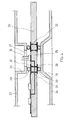
- part of the printed circuit board -8- is fully or partially contained inside two electromagnetic protecting enclosure components -9- and -10- which have electrical conduction characteristics and which sandwich, the circuit board and which contain, inside them, all the electronic components integrated in the printed circuit, in such a way that the said printed circuit continues into a part -8'- which is arranged on the outside of the enveloping enclosure -9-10-, the said zone being intended to receive the connectors which are indicated, in a diagrammatic manner, by the numeral -11-.
- the filtering of the conductors for example the conductor -12-, is carried out inside the enveloping electromagnetic protecting enclosure -9-10-, electronic filtering elements -13- and -14- having been illustrated diagrammatically.
- a longitudinal opening or groove -16- is formed through which the printed circuit board passes and which has coupled to it at the top and bottom individual conducting zones -17- and -18- which are produced, for example, by means of copper or other suitable metal.
- conductive joints such as -19- and -20- are provided which make contact, respectively, with the upper and lower conducting zones -17- and -18- and the edges of the enveloping enclosure.
- interconnecting conductors may be arranged, if needed, which are illustrated by the numerals -21- and -22- in Figure 2 and which are normally aligned along the groove, as will be noted in Figure 3 in which can be seen the conducting elements -22-, -22'-, -22''-, ..., which are variable in number and determine intermediate windows of small dimensions such as -23-, -23'-, -23''-, ..., through which the conductors originating from the internal zone of the printed circuit and from the filtering systems will pass.
- the said conductors have been illustrated diagrammatically by the numeral -12- in Figure 2, and are finally connected into the ordinary connections -11- arranged on the outside of the enveloping enclosure -9-10-.
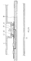
- the connectors -24- are disposed in an intermediate zone -25- on the printed circuit board (PCB) -26-, which permits better adaptation to certain types of apparatus.
- the electromagnetic insulation of the intermediate zone -25- is effected by means of the upper and lower conducting areas -27- and -28-, which will assume the form of closed loops on each face of the printed circuit board -25-, which receive individual conductive joints -29- and -30- which are similar to those in the preferred embodiment of the present invention.
- interconnecting conductors if needed, such as -31- and -32- in a similar manner to the main version.
- the upper wall -33- and lower wall -34- making up the enveloping enclosure of the electronic apparatus are shown with individual inset portions or concave zones -35- and -36- in order to reach the level corresponding to the joints -29- and -30-, the bottom of the concavity -35- having an aperture -37- intended for the passage of the connectors.
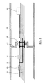
- FIG. 5 This constructional variant also may be achieved as shown in Figure 5, in which can be seen elements equivalent to those in Figure 4 in the upper part of the envelope of the PCB, and which shows the PCB, which is indicated in this case by the numeral -38-, and the connector -39- located in the bottom of a concavity -40- in the upper wall -41- of the envelope of the panel, there being a single conductive joint -42- and a single contact part in the upper face of the PCB -38-, which is indicated by the numeral -43-.
- the invention is also applicable to the case in which it is desired to separate the elements of a printed circuit board in two sections, one of them containing more delicate components and being electromagnetically protected from the other section of the circuit board or "noisy" section by the same arrangements as for separating the two previously explained zones -8- and -8'-.
- This embodiment which has been shown in figure 6, features a second enveloping enclosure -45- which eventually may be a part of the enveloping enclosure -10- for section -8-.
- the second enveloping enclosure protects the components -46- of the printed circuit board which is desired to protect from the "noisy" section of components contained in zone -8-.
- the filtering means represented by the same references -13- and -14- as above explained will protect components -46- from emissions coming from said "noisy" section.
- the enveloping enclosure is the same for both parts of the circuit board, there will be an internal wall -47- in the common enclosure through which the circuit board will pass with the same closing and contact arrangements as explained for figures 1 and successive.
- the same principles and means for attenuation of electromagnetic interference which have been disclosed in the aforegoing may be used for the protection of the components in the printed circuit board from disturbances entering from the outside, through the conductors, that is, the reverse of the aforegoing teaching in which the filtering means were arranged to avoid the electromagnetic disturbances generated by the elements on the printed circuit board within the enclosure from being transmitted via the conductors passing through the enclosure to the external connectors.
- the filtering means represented by numeral references -49- and -50- are arranged on the external part -8'- of the circuit board protecting the electronic devices -51- inside of the enclosure -9-, -10- against electromagnetic disturbances which might be channelled by the conductors -52- from the outside to the internal elements contained within the enclosure -9-, -10-.
- the enveloping electromagnetic protecting enclosure is effectively continuous in the apertures for the passage of the conductors to the outside.
- connections made in the upper and lower output parts of the printed circuit have the benefit of a number of easily designed implementations.
- connections are arranged outside the protective enclosure and allow great flexibility of design, facilitate the changing of connectors used and are also remarkably simple and easy to manufacture and assemble to.
- This arrangement also makes it possible to achieve the separation of two clearly differentiated zones of the same PCB, one of them being an electromagnetically noisy or dirty zone and situated inside the protective enclosure and the other, which is basically electromagnetically quiet or clean, being the one which corresponds to that part of the printed circuit which is located outside the actual electromagnetic protecting enclosure.
- An additional sealing function can be obtained by the use of suitable commercially available gaskets which provide a sealing function in addition to electrical contact.
Landscapes
- Engineering & Computer Science (AREA)
- Microelectronics & Electronic Packaging (AREA)
- Shielding Devices Or Components To Electric Or Magnetic Fields (AREA)
- Noise Elimination (AREA)
Claims (9)
- Dispositif protégeant des interférences électromagnétiques dans des appareils électroniques comportant une plaquette à circuits imprimés, dispositif dans lequel :(a) la plaquette à circuits imprimés comprend deux types de zones :un premier type de zone (8) avec des sources d'énergie haute fréquence et qui est situé à l'intérieur d'un bouclier ou protection enveloppante conductrice électriquement (9, 10) conçu pour empêcher ou atténuer le rayonnement électromagnétique direct, etun second type de zone (8') qui est électriquement connecté à la première zone par des conducteurs (12) qui n'est pas logé dans la même protection ou partie de protection contenant le premier type de zone (8) permettant la connexion à d'autres dispositifs,(b) des moyens de filtration (13, 14) incorporés dans la plaquette à circuits et qui sont conçus pour enlever ou atténuer l'énergie haute fréquence indésirable des conducteurs (12) qui relient les deux zones (8, 8'), et(c) une connexion électrique haute fréquence (19, 20) entre les moyens de filtration (13, 14) et la protection (9, 10) est disposée à la ou aux limites de deux différents types de zones de la plaquette à circuits imprimés (8, 8').
- Dispositif selon la revendication 1, dans lequel la zone du second type (8') est située à l'extérieur de la protection enveloppante (9, 10).
- Dispositif selon la revendication 1, dans lequel la connexion entre les moyens de filtrage (13, 14) et la protection (9, 10) s'effectue par des zones conductrices (17, 18) sur les faces supérieures et/ou inférieures de la plaquette à circuits imprimés à la limite des deux types de zones (8,8').
- Dispositif selon la revendication 3, dans lequel les zones conductrices (17, 18) sont reliées entre elles électriquement au moyen d'éléments conducteurs transversaux (21, 22, 22' ...).
- Dispositif selon les revendications 1 à 4, dans lequel le contact mécanique électrique entre la protection (9, 10) et les zones conductrices (17, 18) est réalisé par l'intermédiaire d'un matériau conducteur souple ou de joints ou plots métalliques (19, 20).
- Dispositif selon les revendications 1 et 2, dans lequel la seconde zone ou les zones (8') sont déterminées par les portions de la plaquette à circuits imprimés qui font saillie à travers la protection.
- Dispositif selon la revendication 1, dans lequel la seconde zone ou les zones (8') sont déterminées par des portions intermédiaires de la plaquette à circuits imprimés qui sont accessibles par des ouvertures formées dans la protection.
- Dispositif selon la revendication 1, dans lequel la seconde zone de la plaquette à circuits imprimés (8') est située dans une protection enveloppante électriquement (45).
- Dispositif selon la revendication 8, dans lequel la protection enveloppante électriquement pour la seconde zone (8') est la même protection (10) que pour la zone (8).
Priority Applications (5)
| Application Number | Priority Date | Filing Date | Title |
|---|---|---|---|
| ES95500098T ES2122491T3 (es) | 1995-02-24 | 1995-07-05 | Dispositivo para impedir interferencias electromagneticas. |
| EP95500098A EP0729294B1 (fr) | 1995-02-24 | 1995-07-05 | Dispositif protégant des interférences électromagnétiques |
| DE69504471T DE69504471T2 (de) | 1995-02-24 | 1995-07-05 | Vorrichtung zur Verhinderung elektromagnetischer Störung |
| US08/602,404 US5684340A (en) | 1995-02-24 | 1996-02-16 | Arrangement for preventing electromagnetic interference |
| JP8029618A JPH08250884A (ja) | 1995-02-24 | 1996-02-16 | 電磁干渉防止装置 |
Applications Claiming Priority (3)
| Application Number | Priority Date | Filing Date | Title |
|---|---|---|---|
| EP95500019 | 1995-02-24 | ||
| EP95500019 | 1995-02-24 | ||
| EP95500098A EP0729294B1 (fr) | 1995-02-24 | 1995-07-05 | Dispositif protégant des interférences électromagnétiques |
Publications (2)
| Publication Number | Publication Date |
|---|---|
| EP0729294A1 EP0729294A1 (fr) | 1996-08-28 |
| EP0729294B1 true EP0729294B1 (fr) | 1998-09-02 |
Family
ID=26140629
Family Applications (1)
| Application Number | Title | Priority Date | Filing Date |
|---|---|---|---|
| EP95500098A Expired - Lifetime EP0729294B1 (fr) | 1995-02-24 | 1995-07-05 | Dispositif protégant des interférences électromagnétiques |
Country Status (5)
| Country | Link |
|---|---|
| US (1) | US5684340A (fr) |
| EP (1) | EP0729294B1 (fr) |
| JP (1) | JPH08250884A (fr) |
| DE (1) | DE69504471T2 (fr) |
| ES (1) | ES2122491T3 (fr) |
Cited By (7)
| Publication number | Priority date | Publication date | Assignee | Title |
|---|---|---|---|---|
| US8538560B2 (en) | 2004-04-29 | 2013-09-17 | Rosemount Inc. | Wireless power and communication unit for process field devices |
| US8626087B2 (en) | 2009-06-16 | 2014-01-07 | Rosemount Inc. | Wire harness for field devices used in a hazardous locations |
| US8694060B2 (en) | 2008-06-17 | 2014-04-08 | Rosemount Inc. | Form factor and electromagnetic interference protection for process device wireless adapters |
| US8787848B2 (en) | 2004-06-28 | 2014-07-22 | Rosemount Inc. | RF adapter for field device with low voltage intrinsic safety clamping |
| US8847571B2 (en) | 2008-06-17 | 2014-09-30 | Rosemount Inc. | RF adapter for field device with variable voltage drop |
| US8929948B2 (en) | 2008-06-17 | 2015-01-06 | Rosemount Inc. | Wireless communication adapter for field devices |
| US9310794B2 (en) | 2011-10-27 | 2016-04-12 | Rosemount Inc. | Power supply for industrial process field device |
Families Citing this family (32)
| Publication number | Priority date | Publication date | Assignee | Title |
|---|---|---|---|---|
| DE19630720A1 (de) * | 1996-07-30 | 1998-02-05 | Bodenseewerk Geraetetech | Filteranordnung zur Trennung eines HF-Felder enthaltenden Bereiches von einem gegen HF-Felder abgeschirmten Bereich |
| US5717577A (en) * | 1996-10-30 | 1998-02-10 | Ericsson, Inc. | Gasketed shield can for shielding emissions of electromagnetic energy |
| DE19649848A1 (de) | 1996-12-02 | 1998-06-04 | Mannesmann Vdo Ag | Elektronischer Schaltkreis mit einem hochfrequenzbedämpfenden Schirmgehäuse |
| JPH11101835A (ja) * | 1997-09-26 | 1999-04-13 | Sharp Corp | Rf通信ユニットおよびその検査方法 |
| US6255581B1 (en) * | 1998-03-31 | 2001-07-03 | Gore Enterprise Holdings, Inc. | Surface mount technology compatible EMI gasket and a method of installing an EMI gasket on a ground trace |
| JP2002530684A (ja) * | 1998-11-24 | 2002-09-17 | コンティネンタル・テーベス・アクチエンゲゼルシヤフト・ウント・コンパニー・オッフェネ・ハンデルスゲゼルシヤフト | 電子機能ユニットおよびまたは機能グループの保護装置 |
| JP2000269678A (ja) * | 1999-03-16 | 2000-09-29 | Matsushita Electric Ind Co Ltd | 高周波装置 |
| US6116924A (en) * | 1999-05-25 | 2000-09-12 | 3Com Corporation | Electromagnetic emissions shielding structure for circuit board connector assembly |
| US6309742B1 (en) | 2000-01-28 | 2001-10-30 | Gore Enterprise Holdings, Inc. | EMI/RFI shielding gasket |
| JP2002094689A (ja) * | 2000-06-07 | 2002-03-29 | Sony Computer Entertainment Inc | プログラム実行システム、プログラム実行装置、中継装置、および記録媒体 |
| CN100433952C (zh) * | 2000-11-30 | 2008-11-12 | 神达电脑股份有限公司 | 抑制高速电路电磁干扰的抵消电路 |
| US6376993B1 (en) * | 2001-02-20 | 2002-04-23 | Perkinelmer Optoelectronics, N.C., Inc. | Power supply to xenon ARC lamp interface |
| US20050095410A1 (en) * | 2001-03-19 | 2005-05-05 | Mazurkiewicz Paul H. | Board-level conformal EMI shield having an electrically-conductive polymer coating over a thermally-conductive dielectric coating |
| US6900383B2 (en) | 2001-03-19 | 2005-05-31 | Hewlett-Packard Development Company, L.P. | Board-level EMI shield that adheres to and conforms with printed circuit board component and board surfaces |
| US6743975B2 (en) | 2001-03-19 | 2004-06-01 | Hewlett-Packard Development Company, L.P. | Low profile non-electrically-conductive component cover for encasing circuit board components to prevent direct contact of a conformal EMI shield |
| FR2840505A1 (fr) * | 2002-05-31 | 2003-12-05 | Thomson Multimedia Broadband F | Dispositif de blindage pour cartes de circuits imprimes |
| DE10228633B4 (de) * | 2002-06-26 | 2006-12-21 | Fujitsu Siemens Computers Gmbh | Vorrichtung zum Schutz vor elektrostatischer Entladung und elektromagnetischer Einflüsse |
| US7209368B2 (en) * | 2003-01-30 | 2007-04-24 | Endicott Interconnect Technologies, Inc. | Circuitized substrate with signal wire shielding, electrical assembly utilizing same and method of making |
| US7326862B2 (en) | 2003-02-13 | 2008-02-05 | Parker-Hannifin Corporation | Combination metal and plastic EMI shield |
| US7005573B2 (en) | 2003-02-13 | 2006-02-28 | Parker-Hannifin Corporation | Composite EMI shield |
| US7478472B2 (en) * | 2004-03-03 | 2009-01-20 | Endicott Interconnect Technologies, Inc. | Method of making circuitized substrate with signal wire shielding |
| US7679005B2 (en) * | 2005-03-23 | 2010-03-16 | Endicott Interconnect Technologies, Inc. | Circuitized substrate with shielded signal lines and plated-thru-holes and method of making same, and electrical assembly and information handling system utilizing same |
| NL1030295C2 (nl) * | 2005-10-28 | 2007-05-03 | Fei Co | Hermetisch afgesloten behuizing met elektrische doorvoer. |
| JP5289712B2 (ja) * | 2007-01-30 | 2013-09-11 | 三菱電機株式会社 | シールドカバー取付け構造および表示装置 |
| ES2354543B1 (es) * | 2009-03-13 | 2012-02-23 | Grin Grupo Ingenieros, S.L | Mesa con protección electromagnética. |
| US9674976B2 (en) | 2009-06-16 | 2017-06-06 | Rosemount Inc. | Wireless process communication adapter with improved encapsulation |
| US10761524B2 (en) | 2010-08-12 | 2020-09-01 | Rosemount Inc. | Wireless adapter with process diagnostics |
| US10007302B2 (en) * | 2016-02-15 | 2018-06-26 | Neocoil, Llc | Magnetic resonance imaging compatible mobile computing device |
| DE102019219478A1 (de) | 2019-12-12 | 2021-06-17 | Continental Automotive Gmbh | Modular erweiterbares elektronisches steuergerät |
| JP7278233B2 (ja) * | 2020-03-19 | 2023-05-19 | 株式会社ソニー・インタラクティブエンタテインメント | 電子機器 |
| EP3886551B1 (fr) * | 2020-03-27 | 2023-05-10 | Hamilton Sundstrand Corporation | Appareil permettant d'atténuer l'interférence électromagnétique dans un contrôleur électronique |
| JP7419963B2 (ja) * | 2020-05-14 | 2024-01-23 | 株式会社デンソー | 電力変換装置 |
Family Cites Families (9)
| Publication number | Priority date | Publication date | Assignee | Title |
|---|---|---|---|---|
| JPH0627995Y2 (ja) * | 1986-03-20 | 1994-07-27 | 株式会社東芝 | シ−ルド構造 |
| CH674288A5 (en) * | 1987-12-02 | 1990-05-15 | Oerlikon Buehrle Ag | Screened electrical equipment with filters built into screen - has sealed opening in wall for connections which pass through screen between inner and outer wiring |
| DE3823469A1 (de) * | 1988-07-11 | 1990-01-18 | Bodenseewerk Geraetetech | Filteranordnung |
| FR2669501B1 (fr) * | 1990-11-16 | 1996-06-21 | Telecommunications Sa | Embase pour coffret blinde de cartes imprimees. |
| CA2116995C (fr) * | 1993-03-05 | 1999-01-12 | Kazunori Yamate | Condensateur a trois bornes et dispositif le comportant |
| JP3087495B2 (ja) * | 1993-03-05 | 2000-09-11 | 松下電器産業株式会社 | コンデンサおよびシールドケース |
| CA2137497A1 (fr) * | 1993-12-09 | 1995-06-10 | Arno Muller | Blindage de confinement de champ electromagnetique pour carte logique principale universelle modulaire |
| DE4407492A1 (de) * | 1994-03-07 | 1995-09-14 | Bodenseewerk Geraetetech | Einrichtung zur Abschirmung von auf einer Elektronikkarte angeordneten elektronischen Bauteilen gegen äußere, elektromagnetische Felder |
| US5428508A (en) * | 1994-04-29 | 1995-06-27 | Motorola, Inc. | Method for providing electromagnetic shielding of an electrical circuit |
-
1995
- 1995-07-05 DE DE69504471T patent/DE69504471T2/de not_active Expired - Lifetime
- 1995-07-05 ES ES95500098T patent/ES2122491T3/es not_active Expired - Lifetime
- 1995-07-05 EP EP95500098A patent/EP0729294B1/fr not_active Expired - Lifetime
-
1996
- 1996-02-16 JP JP8029618A patent/JPH08250884A/ja active Pending
- 1996-02-16 US US08/602,404 patent/US5684340A/en not_active Expired - Lifetime
Cited By (7)
| Publication number | Priority date | Publication date | Assignee | Title |
|---|---|---|---|---|
| US8538560B2 (en) | 2004-04-29 | 2013-09-17 | Rosemount Inc. | Wireless power and communication unit for process field devices |
| US8787848B2 (en) | 2004-06-28 | 2014-07-22 | Rosemount Inc. | RF adapter for field device with low voltage intrinsic safety clamping |
| US8694060B2 (en) | 2008-06-17 | 2014-04-08 | Rosemount Inc. | Form factor and electromagnetic interference protection for process device wireless adapters |
| US8847571B2 (en) | 2008-06-17 | 2014-09-30 | Rosemount Inc. | RF adapter for field device with variable voltage drop |
| US8929948B2 (en) | 2008-06-17 | 2015-01-06 | Rosemount Inc. | Wireless communication adapter for field devices |
| US8626087B2 (en) | 2009-06-16 | 2014-01-07 | Rosemount Inc. | Wire harness for field devices used in a hazardous locations |
| US9310794B2 (en) | 2011-10-27 | 2016-04-12 | Rosemount Inc. | Power supply for industrial process field device |
Also Published As
| Publication number | Publication date |
|---|---|
| DE69504471D1 (de) | 1998-10-08 |
| EP0729294A1 (fr) | 1996-08-28 |
| JPH08250884A (ja) | 1996-09-27 |
| ES2122491T3 (es) | 1998-12-16 |
| US5684340A (en) | 1997-11-04 |
| DE69504471T2 (de) | 1999-04-29 |
Similar Documents
| Publication | Publication Date | Title |
|---|---|---|
| EP0729294B1 (fr) | Dispositif protégant des interférences électromagnétiques | |
| US4829432A (en) | Apparatus for shielding an electrical circuit from electromagnetic interference | |
| US8077480B2 (en) | Faraday cage for camera | |
| US4945323A (en) | Filter arrangement | |
| US5268810A (en) | Electrical connector incorporating EMI filter | |
| US6650203B2 (en) | Filter arrangement | |
| US5266054A (en) | Sealed and filtered header receptacle | |
| US9190837B2 (en) | Rigid flex electromagnetic pulse protection device | |
| KR970705200A (ko) | 차폐된 커넥터 및 도금된 구멍들을 갖는 보드의 조립체(Assembly of Shielded Connectors and a Board Having Plated Holes) | |
| EP0424606B1 (fr) | Boîtier modulaire pour deux circuits incompatibles | |
| EP0610476B1 (fr) | Ensemble ecran pour plaquette de circuits imprimes | |
| US6140575A (en) | Shielded electronic circuit assembly | |
| EP3240387B1 (fr) | Blindage électromagnétique pour un dispositif électronique | |
| US5253146A (en) | Earthed intermediate frame for circuit boards | |
| US5604668A (en) | Apparatus for shielding electronic circuit boards | |
| US5610368A (en) | Clip plate bulkhead mounting for EMI filters | |
| US5130896A (en) | Apparatus for electromagnetic interference containment for printed circuit board connectors | |
| US5285007A (en) | System for reducing the emission of high frequency electromagnetic waves from computer systems | |
| EP0534372B1 (fr) | Filtre d'interferences électromagnétique et blindage pour une plaque de circuit imprimé | |
| EP3886551B1 (fr) | Appareil permettant d'atténuer l'interférence électromagnétique dans un contrôleur électronique | |
| KR970001779Y1 (ko) | 전자파 시일드(shield)형 회로 유니트 | |
| US7912328B2 (en) | Optical waveguide EMI shield | |
| JPH08148877A (ja) | 電子機器用遮蔽装置 | |
| US5386204A (en) | High isolation microwave module | |
| JP2692615B2 (ja) | 高周波回路装置 |
Legal Events
| Date | Code | Title | Description |
|---|---|---|---|
| PUAI | Public reference made under article 153(3) epc to a published international application that has entered the european phase |
Free format text: ORIGINAL CODE: 0009012 |
|
| AK | Designated contracting states |
Kind code of ref document: A1 Designated state(s): DE ES FR GB IT |
|
| 17P | Request for examination filed |
Effective date: 19970225 |
|
| GRAG | Despatch of communication of intention to grant |
Free format text: ORIGINAL CODE: EPIDOS AGRA |
|
| GRAG | Despatch of communication of intention to grant |
Free format text: ORIGINAL CODE: EPIDOS AGRA |
|
| GRAH | Despatch of communication of intention to grant a patent |
Free format text: ORIGINAL CODE: EPIDOS IGRA |
|
| 17Q | First examination report despatched |
Effective date: 19980123 |
|
| GRAH | Despatch of communication of intention to grant a patent |
Free format text: ORIGINAL CODE: EPIDOS IGRA |
|
| GRAA | (expected) grant |
Free format text: ORIGINAL CODE: 0009210 |
|
| AK | Designated contracting states |
Kind code of ref document: B1 Designated state(s): DE ES FR GB IT |
|
| REF | Corresponds to: |
Ref document number: 69504471 Country of ref document: DE Date of ref document: 19981008 |
|
| REG | Reference to a national code |
Ref country code: ES Ref legal event code: FG2A Ref document number: 2122491 Country of ref document: ES Kind code of ref document: T3 |
|
| ET | Fr: translation filed | ||
| PLBE | No opposition filed within time limit |
Free format text: ORIGINAL CODE: 0009261 |
|
| STAA | Information on the status of an ep patent application or granted ep patent |
Free format text: STATUS: NO OPPOSITION FILED WITHIN TIME LIMIT |
|
| 26N | No opposition filed | ||
| REG | Reference to a national code |
Ref country code: GB Ref legal event code: IF02 |
|
| REG | Reference to a national code |
Ref country code: GB Ref legal event code: 732E |
|
| REG | Reference to a national code |
Ref country code: FR Ref legal event code: TP |
|
| PGFP | Annual fee paid to national office [announced via postgrant information from national office to epo] |
Ref country code: ES Payment date: 20050727 Year of fee payment: 11 |
|
| PGFP | Annual fee paid to national office [announced via postgrant information from national office to epo] |
Ref country code: IT Payment date: 20060731 Year of fee payment: 12 |
|
| REG | Reference to a national code |
Ref country code: ES Ref legal event code: FD2A Effective date: 20060706 |
|
| PG25 | Lapsed in a contracting state [announced via postgrant information from national office to epo] |
Ref country code: ES Free format text: LAPSE BECAUSE OF NON-PAYMENT OF DUE FEES Effective date: 20060706 |
|
| PGFP | Annual fee paid to national office [announced via postgrant information from national office to epo] |
Ref country code: FR Payment date: 20070717 Year of fee payment: 13 |
|
| REG | Reference to a national code |
Ref country code: FR Ref legal event code: ST Effective date: 20090331 |
|
| PG25 | Lapsed in a contracting state [announced via postgrant information from national office to epo] |
Ref country code: FR Free format text: LAPSE BECAUSE OF NON-PAYMENT OF DUE FEES Effective date: 20080731 |
|
| PG25 | Lapsed in a contracting state [announced via postgrant information from national office to epo] |
Ref country code: IT Free format text: LAPSE BECAUSE OF NON-PAYMENT OF DUE FEES Effective date: 20070705 |
|
| REG | Reference to a national code |
Ref country code: GB Ref legal event code: 732E Free format text: REGISTERED BETWEEN 20120329 AND 20120404 |
|
| PGFP | Annual fee paid to national office [announced via postgrant information from national office to epo] |
Ref country code: GB Payment date: 20130626 Year of fee payment: 19 |
|
| PGFP | Annual fee paid to national office [announced via postgrant information from national office to epo] |
Ref country code: DE Payment date: 20130621 Year of fee payment: 19 |
|
| REG | Reference to a national code |
Ref country code: DE Ref legal event code: R119 Ref document number: 69504471 Country of ref document: DE |
|
| GBPC | Gb: european patent ceased through non-payment of renewal fee |
Effective date: 20140705 |
|
| PG25 | Lapsed in a contracting state [announced via postgrant information from national office to epo] |
Ref country code: DE Free format text: LAPSE BECAUSE OF NON-PAYMENT OF DUE FEES Effective date: 20150203 |
|
| REG | Reference to a national code |
Ref country code: DE Ref legal event code: R119 Ref document number: 69504471 Country of ref document: DE Effective date: 20150203 |
|
| PG25 | Lapsed in a contracting state [announced via postgrant information from national office to epo] |
Ref country code: GB Free format text: LAPSE BECAUSE OF NON-PAYMENT OF DUE FEES Effective date: 20140705 |