EP0730186A1 - Structure et méthode de circuit imprimé et dispositif à cristaux liquides utilisant la structure de connexion - Google Patents
Structure et méthode de circuit imprimé et dispositif à cristaux liquides utilisant la structure de connexion Download PDFInfo
- Publication number
- EP0730186A1 EP0730186A1 EP96301386A EP96301386A EP0730186A1 EP 0730186 A1 EP0730186 A1 EP 0730186A1 EP 96301386 A EP96301386 A EP 96301386A EP 96301386 A EP96301386 A EP 96301386A EP 0730186 A1 EP0730186 A1 EP 0730186A1
- Authority
- EP
- European Patent Office
- Prior art keywords
- lead electrodes
- connection structure
- electrodes
- circuit member
- substrate
- Prior art date
- Legal status (The legal status is an assumption and is not a legal conclusion. Google has not performed a legal analysis and makes no representation as to the accuracy of the status listed.)
- Granted
Links
Images



Classifications
-
- H—ELECTRICITY
- H05—ELECTRIC TECHNIQUES NOT OTHERWISE PROVIDED FOR
- H05K—PRINTED CIRCUITS; CASINGS OR CONSTRUCTIONAL DETAILS OF ELECTRIC APPARATUS; MANUFACTURE OF ASSEMBLAGES OF ELECTRICAL COMPONENTS
- H05K3/00—Apparatus or processes for manufacturing printed circuits
- H05K3/46—Manufacturing multilayer circuits
-
- G—PHYSICS
- G02—OPTICS
- G02F—OPTICAL DEVICES OR ARRANGEMENTS FOR THE CONTROL OF LIGHT BY MODIFICATION OF THE OPTICAL PROPERTIES OF THE MEDIA OF THE ELEMENTS INVOLVED THEREIN; NON-LINEAR OPTICS; FREQUENCY-CHANGING OF LIGHT; OPTICAL LOGIC ELEMENTS; OPTICAL ANALOGUE/DIGITAL CONVERTERS
- G02F1/00—Devices or arrangements for the control of the intensity, colour, phase, polarisation or direction of light arriving from an independent light source, e.g. switching, gating or modulating; Non-linear optics
- G02F1/01—Devices or arrangements for the control of the intensity, colour, phase, polarisation or direction of light arriving from an independent light source, e.g. switching, gating or modulating; Non-linear optics for the control of the intensity, phase, polarisation or colour
- G02F1/13—Devices or arrangements for the control of the intensity, colour, phase, polarisation or direction of light arriving from an independent light source, e.g. switching, gating or modulating; Non-linear optics for the control of the intensity, phase, polarisation or colour based on liquid crystals, e.g. single liquid crystal display cells
- G02F1/133—Constructional arrangements; Operation of liquid crystal cells; Circuit arrangements
- G02F1/1333—Constructional arrangements; Manufacturing methods
- G02F1/1345—Conductors connecting electrodes to cell terminals
- G02F1/13452—Conductors connecting driver circuitry and terminals of panels
-
- H—ELECTRICITY
- H05—ELECTRIC TECHNIQUES NOT OTHERWISE PROVIDED FOR
- H05K—PRINTED CIRCUITS; CASINGS OR CONSTRUCTIONAL DETAILS OF ELECTRIC APPARATUS; MANUFACTURE OF ASSEMBLAGES OF ELECTRICAL COMPONENTS
- H05K3/00—Apparatus or processes for manufacturing printed circuits
- H05K3/36—Assembling printed circuits with other printed circuits
- H05K3/361—Assembling flexible printed circuits with other printed circuits
-
- H—ELECTRICITY
- H05—ELECTRIC TECHNIQUES NOT OTHERWISE PROVIDED FOR
- H05K—PRINTED CIRCUITS; CASINGS OR CONSTRUCTIONAL DETAILS OF ELECTRIC APPARATUS; MANUFACTURE OF ASSEMBLAGES OF ELECTRICAL COMPONENTS
- H05K3/00—Apparatus or processes for manufacturing printed circuits
- H05K3/36—Assembling printed circuits with other printed circuits
- H05K3/361—Assembling flexible printed circuits with other printed circuits
- H05K3/363—Assembling flexible printed circuits with other printed circuits by soldering
-
- H—ELECTRICITY
- H05—ELECTRIC TECHNIQUES NOT OTHERWISE PROVIDED FOR
- H05K—PRINTED CIRCUITS; CASINGS OR CONSTRUCTIONAL DETAILS OF ELECTRIC APPARATUS; MANUFACTURE OF ASSEMBLAGES OF ELECTRICAL COMPONENTS
- H05K2201/00—Indexing scheme relating to printed circuits covered by H05K1/00
- H05K2201/03—Conductive materials
- H05K2201/0332—Structure of the conductor
- H05K2201/0388—Other aspects of conductors
- H05K2201/0394—Conductor crossing over a hole in the substrate or a gap between two separate substrate parts
-
- H—ELECTRICITY
- H05—ELECTRIC TECHNIQUES NOT OTHERWISE PROVIDED FOR
- H05K—PRINTED CIRCUITS; CASINGS OR CONSTRUCTIONAL DETAILS OF ELECTRIC APPARATUS; MANUFACTURE OF ASSEMBLAGES OF ELECTRICAL COMPONENTS
- H05K2203/00—Indexing scheme relating to apparatus or processes for manufacturing printed circuits covered by H05K3/00
- H05K2203/01—Tools for processing; Objects used during processing
- H05K2203/0195—Tool for a process not provided for in H05K3/00, e.g. tool for handling objects using suction, for deforming objects, for applying local pressure
-
- H—ELECTRICITY
- H05—ELECTRIC TECHNIQUES NOT OTHERWISE PROVIDED FOR
- H05K—PRINTED CIRCUITS; CASINGS OR CONSTRUCTIONAL DETAILS OF ELECTRIC APPARATUS; MANUFACTURE OF ASSEMBLAGES OF ELECTRICAL COMPONENTS
- H05K3/00—Apparatus or processes for manufacturing printed circuits
- H05K3/30—Assembling printed circuits with electric components, e.g. with resistors
- H05K3/32—Assembling printed circuits with electric components, e.g. with resistors electrically connecting electric components or wires to printed circuits
- H05K3/321—Assembling printed circuits with electric components, e.g. with resistors electrically connecting electric components or wires to printed circuits by conductive adhesives
- H05K3/323—Assembling printed circuits with electric components, e.g. with resistors electrically connecting electric components or wires to printed circuits by conductive adhesives by applying an anisotropic conductive adhesive layer over an array of pads
-
- H—ELECTRICITY
- H05—ELECTRIC TECHNIQUES NOT OTHERWISE PROVIDED FOR
- H05K—PRINTED CIRCUITS; CASINGS OR CONSTRUCTIONAL DETAILS OF ELECTRIC APPARATUS; MANUFACTURE OF ASSEMBLAGES OF ELECTRICAL COMPONENTS
- H05K3/00—Apparatus or processes for manufacturing printed circuits
- H05K3/30—Assembling printed circuits with electric components, e.g. with resistors
- H05K3/32—Assembling printed circuits with electric components, e.g. with resistors electrically connecting electric components or wires to printed circuits
- H05K3/34—Assembling printed circuits with electric components, e.g. with resistors electrically connecting electric components or wires to printed circuits by soldering
- H05K3/3452—Solder masks
-
- H—ELECTRICITY
- H05—ELECTRIC TECHNIQUES NOT OTHERWISE PROVIDED FOR
- H05K—PRINTED CIRCUITS; CASINGS OR CONSTRUCTIONAL DETAILS OF ELECTRIC APPARATUS; MANUFACTURE OF ASSEMBLAGES OF ELECTRICAL COMPONENTS
- H05K3/00—Apparatus or processes for manufacturing printed circuits
- H05K3/30—Assembling printed circuits with electric components, e.g. with resistors
- H05K3/32—Assembling printed circuits with electric components, e.g. with resistors electrically connecting electric components or wires to printed circuits
- H05K3/34—Assembling printed circuits with electric components, e.g. with resistors electrically connecting electric components or wires to printed circuits by soldering
- H05K3/3465—Application of solder
- H05K3/3473—Plating of solder
Definitions
- the present invention relates to a structure and a method of circuit board connection used in various electronic circuits as used in computer main frame and peripheral equipments, etc.
- a conventional circuit board connection structure used in flat display devices having display electrodes arranged in the form of a matrix, such as EL display panels and liquid crystal display panels of the simple matrix-type and the active matrix-type, has been formed by connecting the connecting electrodes on a glass substrate or a plastic substrate of a display device and the output lead electrodes of a type carrier package (TCP) formed by the TAB (tape automated bonding) method by hot-pressure bonding and by connecting the input lead electrodes of the TCP and the connecting electrodes of a print circuit board (PCB, hereinafter sometimes called "PCB board") by solder bonding.
- TAB type carrier package
- PCB print circuit board
- output lead electrodes 6 of a TCP 2 are formed by patterning on a base film and connected to connecting electrodes 11 of a glass substrate 1b with ACF (anisotropic conductive film) 12 as shown in Figure 11, wherein 5 denotes a resin coating and 20 denotes a sealant.
- input lead electrodes 7 of the TCP 2 are exposed locally to an opening formed by locally removing the base film and fixed by soldering to a solder land 10 of connecting electrodes of the PCB 4 as shown in Figure 12 wherein 8 denotes a solder resist.
- the part G of the TCP 2 connected to the glass substrate 1b receiving a concentrated stress and the exposed part G of the TCP 2 connected to the solder land 10 of the PCB board connecting electrodes and receiving a concentrated stress are liable to be broken to cause connection failure.
- the connecting part between a semiconductor chip mounted on the TCP and the connecting electrodes (inner leads) of the TCP is liable to be damaged to cause a connection failure.
- the bonding connection between the output lead electrodes of the TCP and the glass substrate is liable to be peeled apart from each other to cause a connection failure.
- a principal object of the present invention is to provide a circuit board connection structure resistant to breakage due to an environmental temperature change, a method of providing such a connection structure, and a liquid crystal device including such a connection structure.
- a circuit board connection structure comprising: a first substrate having a first electrode pattern, a second substrate having a second electrode pattern, and a film circuit member electrically connecting the first and second electrode patterns, wherein said film circuit member comprises lead electrodes having an exposed portion partly connected to the first electrode pattern at a part of the exposed portion closer to an edge of the film circuit member.
- the film circuit member is provided with an exposed lead electrode which is exposed to an opening formed by removing a portion of the film substrate of the film circuit member, and the exposed lead electrode is partly used for electrical connection to leave an unconnected portion so that, even if a shearing stress occurs in the film circuit member (TCP) due to a difference in thermal expansion between the first and second substrates (a glass substrate and a PCB board), a breakage or connection failure of the film circuit member can be prevented owing to deformation and stretching allowance of the unconnected lead electrode portion.
- TCP film circuit member
- Figure 1 is a partial perspective view of an electronic device including a circuit board connection structure according to an embodiment of the invention.
- Figure 2 is a partial sectional view of the connection structure shown in Figure 1.
- Figure 3 is a schematic plan view of a liquid crystal display device including a circuit board connection structure according to an embodiment of the invention, including a connection of a liquid crystal panel and a PCB board with a film circuit member.
- Figure 4 is an enlarged partial view showing the connection structure at a portion A shown in Figure 3.
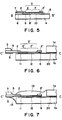
- Figure 5 is a sectional view taken along a B-B' line in Figure 4.
- Figure 6 is a sectional view taken along an A-A' line in Figure 4.
- Figure 7 is a sectional view of a connection structure shown in Figure 6 further including a resin covering a connection between the film circuit member and the glass substrate.
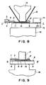
- Figure 8 is a sectional view for illustrating a manner of connecting the output lead electrodes of the film circuit member and the electrode pattern on the glass substrate.
- Figure 9 is a sectional view for illustrating a manner of connecting the input lead electrodes of the film circuit member and the electrode pattern on the PCB board.
- Figure 10 is a sectional view showing a circuit board connection structure according to the invention wherein the PCB board having an electrode soldering part having a height larger than that of an adjacent solder resist.
- Figure 11 is a sectional view showing a conventional circuit board connection structure showing a breakage of an input lead electrode of a film circuit member at a connection with a PCB board.
- Figure 12 is a sectional view showing a conventional circuit board connection structure showing a breakage of an output lead electrode of a film circuit member at a connection with a glass substrate.
- Figure 1 is a partial sectional view of an electronic device (liquid crystal device) including a circuit board connection structure according to an embodiment of the present invention
- Figure 2 is a partial sectional view of the connection structure.
- the circuit board connection structure includes a first substrate 1 having thereon a first electrode pattern 11, a second substrate 4 having thereon a second electrode pattern 9, and a film circuit member 2 directly or indirectly connecting the first electrode pattern and the second electrode pattern.
- indirect connection refers to a mode of connection wherein the first electrode pattern 11 is connected to the second electrode pattern 9 via an integrated circuit mounted on the film circuit member 2.
- the film circuit member 2 includes a laminated structure comprising at least an electrode pattern forming lead electrodes, and an insulating flexible film substrate comprising a relatively hard resin, such as polyester, polyimide or glass-reinforced epoxy resin.
- the film circuit member 2 is provided with openings OP on both sides of connection with the electrode patterns 11 and 9, at which the insulating film is removed to expose the lead electrodes thereat and leave an insulating film portion 2' covering the end portions of the lead electrodes.
- the openings OP are provided in the form of an elongated hole elongated in a direction X in which lead electrodes are arranged (i.e., in a direction perpendicular to a direction Y in which the lead electrodes extend).
- First lead electrodes 6 are connected to the first electrode pattern 11 with a first connecting member 12.
- Second lead electrodes 7 are connected to the second electrode pattern 9 with a second connecting member 10.
- the first and second connecting members 12 and 10 are disposed only at a region F close to the ends of the lead electrodes and not at an inner region E of the exposed lead electrode portion.
- the unconnected region E of the lead electrodes functions as a buffer or allowance for flexural deformation of the lead electrodes or the film circuit member.
- the first and second substrates 1 and 4 may preferably comprise a rigid sheet material, such as a silicon plate, a quartz plate, a ceramic plate, a sapphire plate, a glass plate, a glass fiber-reinforced epoxy resin, or a polyimide resin plate.
- a rigid sheet material such as a silicon plate, a quartz plate, a ceramic plate, a sapphire plate, a glass plate, a glass fiber-reinforced epoxy resin, or a polyimide resin plate.
- the first and second connecting members 12 and 10 may comprise an electroconductive material, such as an anisotropic conductive adhesive of a thermoplastic-type, a thermosetting-type or a photosetting or photocurable-type, or solder.
- the unconnected exposed portion may have a length E which is desirably at least D/5, preferably at least D/4 and at most D/2, preferably at most 2D/5.
- One of the lead electrodes 6 and 7 subjected to a relatively small degree of deformation can be connected without leaving an unconnected exposed part E.
- FIG. 3 is a plan view of such a liquid crystal device, including a circuit board connection structure as described above, e.g., at a part A therein.
- Figure 3 shows a state wherein glass substrates 1a and 1b of the liquid crystal display device is connected with a film circuit member 2 carrying thereon a semiconductor chip 3 for driving the liquid crystal device, and the film circuit member is connected with a glass-epoxy PCB board 4.
- the liquid crystal display device includes a display area 19 at which a liquid crystal is disposed between the substrates 1a and 1b.
- the liquid crystal used in the present invention may preferably comprise a chiral smectic liquid crystal showing ferroelectricity or antiferroelectricity, or a chiral nematic liquid crystal showing two quasi-stable states.
- the liquid crystal device can be of a type in which only one of two substrates is provided with electrodes for supplying an electric field applied to the liquid crystal.
- Figure 4 is a plan view of a connection structure suitably used at part A in Figure 3.
- Figure 4 shows only several tens of output lead electrodes but an actual liquid crystal device may include several hundreds or more of output lead electrodes.
- connection electrodes i.e., scanning electrodes or data electrodes of an electrode matrix
- the film substrate (insulating film) of the film circuit member 2 is removed to provide an opening at which the output lead electrodes 6 alone are connected to the connection electrodes 11.
- the input lead electrodes 7 of the film circuit member exposed by provision of an opening of the film circuit member 2 are connected by soldering onto solder-plated connecting electrodes on the glass-epoxy PCB board 4.
- a film substrate 2' is left unremoved at end portions of the lead electrodes.
- Figures 5 and 6 are sectional views taken along B-B' line and C-C' line, respectively, in Figure 4, for further illustrating the circuit board connection structure according to this embodiment.
- the input lead electrodes 7 of the film circuit member 2 are exposed through an opening of the film substrate at a range D.
- the connection electrodes 9 on the PCB board 4 are exposed through an opening of a solder resist 8 (of, e.g., melamine resin or epoxy resin for protection of surrounding members during soldering or provision of solder by plating) and instead provided with a plated solder 10 at a part corresponding to the near end region F of the input lead electrodes 7 of the film circuit member 2.
- a solder resist 8 of, e.g., melamine resin or epoxy resin for protection of surrounding members during soldering or provision of solder by plating
- the input lead electrodes 7 of the film circuit member 2 are fixed by connection with the solder 10 only at the region F while leaving the unconnected exposed region of the lead electrons 7 at the region E.
- solder is used as the connecting member, but an anisotropic conductive adhesive can also be used to exhibit similar effects.
- the output lead electrodes 6 of the film circuit member 2 are exposed through an opening of the substrate film at a range D'.
- connection electrodes 11 on the glass substrate 1b are coated in advance with an anisotropic conductive adhesive film 12 at a part corresponding to the near end region F' of the output lead electrodes 6 of the film circuit member 2.
- Figure 6 also shows a resin coating 5 (of, e.g., epoxy-phenolic resin, optionally containing silica filler, for protecting the IC chip 3 and lead electrodes 6).
- a resin coating 5 of, e.g., epoxy-phenolic resin, optionally containing silica filler, for protecting the IC chip 3 and lead electrodes 6.
- Figure 7 shows a modification of the connection structure shown in Figure 6, wherein the electrode connection part is covered with a silicone resin coating 13 so as to improve the corrosion resistance and reinforce the electrodes 6, thereby providing an improved reliability of the connection structure.
- the unconnected exposed portion E' of the electrodes 6 is coated with the silicone resin 13
- the unconnected portion E' of the electrodes 6 is deformable if the silicone resin 13 has a rubber hardness of at most 50 deg., thereby relaxing a deformation stress applied to the film circuit member 2.
- the resin coating 13 can also comprise an elastomeric resin having a hardness (JIS A rubber hardness) of at most 50 deg. other than silicone resin.
- the resin coating 13 may preferably comprise an elastomeric resin having a rubber hardness (JIS A) of at most 50 deg., including silicone resin (such as “SE 9140", “PRX 305" and “SE 5004 (trade name)", available from Toray Silicone K.K.), as a preferred example.
- a resin coating 13 is much more resilient than the resin constituting the substrate of the film circuit member 2 comprising, e.g., polyester, polyimide or glass-epoxy resin.
- the rubber hardness of at most 50 deg. roughly corresponds to a Shore hardness of 30A - 60A which is much lower than Shore hardness of 90A - 70D of polyester resin, a relatively soft substrate material.
- Figures 8 and 9 illustrate manners for electrode connection to provide a circuit board connection structure according to the present invention.
- Figure 8 illustrates a method of providing a circuit board connection structure shown in Figure 6.
- an anisotropic conductive adhesive film 12 is placed in advance on the connecting electrodes 11 on the glass substrate 1b at a portion corresponding to the near end region F' ( Figure 6) of the output lead electrodes 6 of the film circuit member 2.
- the superposed electrode structure at a position corresponding to the region F' is heated via a pressing sheet 15 by a heat-press bonding head 14 heated to 150 - 300 °C, thereby bonding the electrodes 6 and 11 with the melted adhesive 12.
- the pressing sheet 15 comprised 0.05 mm-thick teflon film ("NITOFLON No. 900 U2", made by Nitto Denko K.K.) and was used for preventing the staining of the heat-press bonding head 14 with the anisotropic conductive adhesive film and for absorbing a slight inclination of the head and minute unevenness of the connecting electrodes to provide an improved reliability.
- NITOFLON No. 900 U2 made by Nitto Denko K.K.
- Figure 9 illustrates a method of providing a circuit board connection structure shown in Figure 5.
- the input lead electrodes 7 of the film circuit member 2 have been locally exposed at an opening by removing the substrate film at a range D ( Figure 5).
- the connecting electrodes 9 of the PCB board 4 are provided with an opening of the solder resist at a part corresponding to the near end region F of the input lead electrodes of the film circuit member 2 and provided with a plated solder 10.
- a flux is applied onto the plated solder 10 on the connecting electrode of the PCB board 4, and a positional alignment is effected so that the portion (at region F in Figure 5) closer to the end portion 2' of the input lead electrodes 7 of the film circuit member 2 is aligned with the portion of the connecting electrodes 9 of the PCB board 4 provided with the plated solder 10.
- the superposed electrode structure sandwiching the solder resist 8' and the solder 10 is heat-pressed via the lead electrodes 7 by a heat-pressure bonding head 17 heated to 200 - 300 °C, thereby fixedly connecting the electrodes 7 and 9.
- the portion E of the lead electrodes 7 is sandwiched between the heat-pressure bonding head 17 and the solder resist 8', so that the melted solder 10 is prevented from flowing up to the region E of the lead electrodes 7, thus preventing the fixation of the lead electrodes 7 at the region E.
- the film circuit member 2 ( Figure 6) was provided with an opening having a width D' of 2.5 mm for exposing the output lead electrodes 6 and the unconnected exposed length E' of the lead electrodes 6 was 0.5 - 1 mm by using the heat-pressure bonding head 14 having a tip width of 1.5 mm ( Figure 8).
- the film circuit member (as shown in Figure 5) was provided with an opening having a width D of 2 mm and the unconnected exposed length E of 0.5 - 1 mm by using a heat-pressure bonding head 17 of 1.2 mm.
- the above values are raised as mere exemplary values and other sizes may also be used within a scope of the present invention.
- Figure 10 shows a state of the connecting electrodes 9 on the PCB board 4 and the input lead electrodes 7 of the film circuit member 2 immediately before the connection therebetween by the heat-pressure bonding head 17 and, as shown, the solder 10 has a height larger than that of the surrounding solder resist 8', whereby a sufficient contact is ensured between the lead electrodes 7 and the solder 10 at the time of the heat-pressure bonding by the head to effect a good connection.
- the circuit board connection structure according to the present invention may be subjected to an elevated temperature of ca. 100 °C for placing the liquid crystal in an isotropic state for alignment of the liquid crystal.
- the circuit board connection structure according to the present invention may be durable against a shearing stress along a side of a glass substrate along which the film circuit members and the PCB board is disposed caused by a difference in thermal expansion occurring due to a temperature difference between room temperature and such an elevated temperature, because of a deformation or elongation allowance at the unconnected exposed portions of the lead electrodes 7 and 6 at the regions E and E'.
- the PCB board 4 was composed of a 4 to 6-layered glass-epoxy board of FR4 grade (according to NEMA standard) showing a thermal expansion coefficient of 0.08 - 0.125 (x10 -2 cm/cm/°C) close to that of the glass substrates 1a and 1b so as to minimize the shearing force occurring in the film circuit member along the side of the glass substrate even in an environmental temperature change from a low temperature (e.g., -20 °C) to a high temperature (e.g., 60 °C).
- a low temperature e.g., -20 °C
- a high temperature e.g. 60 °C
- such a multi-layer glass-epoxy board of FR4 is liable to cause a heat-shrinkage of 0.02 - 0.025 % at an elevated temperature, which is liable to increase the shearing force occurring in the film circuit member along a side of glass substrate.
- the film circuit member 2 is provided with an opening both with respect to the input lead electrodes and the output lead electrodes, it is possible to provide such an opening to only one side of the input and output lead electrodes.
- the film circuit member 2 is provided with an opening by removal of the film substrate thereof to expose metal lead electrodes, of which only a portion close to the connection is connected to leave a farther unconnected exposed metal lead portion.
- the unconnected exposed portion of the lead electrodes retains a deformation allowance in a direction of arrangement of the lead electrodes at a region E or E' (in Figure 5 or 6) and an elongation allowance in the direction of extension thereof at a region E or E' (in Figure 5 or 6).
- the input lead electrodes 7 of the film circuit member 2 and the solder lands 10 on the connecting electrodes 9 on the PCB board 4 are arranged in rows in a direction perpendicular to a side of the glass substrate 1b.
- the input lead electrodes 7 of the film circuit member 2 are supplied with a pulling force.
- the input lead electrode 7 are provided with an unconnected portion rich in deformation and elongation allowance according to the present invention, so that breakage of the lead electrodes or a connection failure of the film circuit member 2 can be obviated.
- the film circuit member is provided with an opening to expose the metal lead electrodes of the film circuit member, of which only a portion close to the connection is connected to leave a farther unconnected portion, so that the unconnected portion absorbs a stress due to a difference in thermal expansion caused by a change in environmental temperature, whereby the breakage of the connections is prevented to provide an improved reliability of the product.
Landscapes
- Engineering & Computer Science (AREA)
- Physics & Mathematics (AREA)
- Manufacturing & Machinery (AREA)
- Microelectronics & Electronic Packaging (AREA)
- Nonlinear Science (AREA)
- Mathematical Physics (AREA)
- Chemical & Material Sciences (AREA)
- Crystallography & Structural Chemistry (AREA)
- General Physics & Mathematics (AREA)
- Optics & Photonics (AREA)
- Combinations Of Printed Boards (AREA)
- Devices For Indicating Variable Information By Combining Individual Elements (AREA)
Applications Claiming Priority (3)
| Application Number | Priority Date | Filing Date | Title |
|---|---|---|---|
| JP4455895 | 1995-03-03 | ||
| JP44558/95 | 1995-03-03 | ||
| JP4455895 | 1995-03-03 |
Publications (2)
| Publication Number | Publication Date |
|---|---|
| EP0730186A1 true EP0730186A1 (fr) | 1996-09-04 |
| EP0730186B1 EP0730186B1 (fr) | 2001-08-29 |
Family
ID=12694836
Family Applications (1)
| Application Number | Title | Priority Date | Filing Date |
|---|---|---|---|
| EP96301386A Expired - Lifetime EP0730186B1 (fr) | 1995-03-03 | 1996-02-29 | Structure et méthode de circuit imprimé et dispositif à cristaux liquides utilisant la structure de connexion |
Country Status (4)
| Country | Link |
|---|---|
| US (1) | US5936850A (fr) |
| EP (1) | EP0730186B1 (fr) |
| KR (1) | KR100204854B1 (fr) |
| DE (1) | DE69614732D1 (fr) |
Cited By (4)
| Publication number | Priority date | Publication date | Assignee | Title |
|---|---|---|---|---|
| EP0989792A3 (fr) * | 1998-09-25 | 2001-08-08 | Siemens Aktiengesellschaft | Feuille polymère pour le collage à des autres feuilles et à des panneaux à circuit |
| WO2006017037A1 (fr) * | 2004-07-08 | 2006-02-16 | 3M Innovative Properties Company | Procédé de connexion d’éléments conducteurs et composante électrique ou électronique munie de pièces connectées selon la méthode de connexion |
| US7742142B2 (en) | 2005-08-09 | 2010-06-22 | Chunghwa Picture Tubes, Ltd. | Display and tape carrier package structure |
| CN108109520A (zh) * | 2016-11-25 | 2018-06-01 | 三星显示有限公司 | 显示设备 |
Families Citing this family (51)
| Publication number | Priority date | Publication date | Assignee | Title |
|---|---|---|---|---|
| US5808707A (en) * | 1995-03-01 | 1998-09-15 | Canon Kabushiki Kaisha | Display apparatus |
| US6357111B1 (en) * | 1997-04-21 | 2002-03-19 | Seiko Epson Corporation | Inter-electrode connection structure, inter-electrode connection method, semiconductor device, semiconductor mounting method, liquid crystal device, and electronic apparatus |
| JPH11167971A (ja) * | 1997-12-05 | 1999-06-22 | Olympus Optical Co Ltd | 電子機器 |
| DE19754874A1 (de) * | 1997-12-10 | 1999-06-24 | Siemens Ag | Verfahren zur Umformung eines Substrats mit Randkontakten in ein Ball Grid Array, nach diesem Verfahren hergestelltes Ball Grid Array und flexible Verdrahtung zur Umformung eines Substrats mit Randkontakten in ein Ball Grid Array |
| KR100476524B1 (ko) * | 1997-12-31 | 2005-08-29 | 삼성전자주식회사 | 엘씨디모듈용테이프캐리어패키지 |
| US6329594B1 (en) * | 1998-01-16 | 2001-12-11 | Bae Systems Information And Electronic Systems Integration, Inc. | Integrated circuit package |
| JP4298068B2 (ja) | 1998-08-18 | 2009-07-15 | セイコーエプソン株式会社 | 電気光学装置およびそれらを備えた電子機器並びに電気光学装置の製造方法 |
| US6971750B1 (en) * | 1998-12-28 | 2005-12-06 | Canon Kabushiki Kaisha | Projection display apparatus |
| JP2000252598A (ja) * | 1999-03-02 | 2000-09-14 | Fuji Photo Film Co Ltd | フレキシブルプリント配線板 |
| US6164984A (en) * | 1999-04-01 | 2000-12-26 | Schreiner Etiketten Und Selbstkelbetechnik Gmbh & Co. | Electrical connecting element |
| JP2001013883A (ja) * | 1999-06-30 | 2001-01-19 | Fujitsu Ltd | ドライバic実装モジュール及びそれを使用した平板型表示装置 |
| US6449836B1 (en) * | 1999-07-30 | 2002-09-17 | Denso Corporation | Method for interconnecting printed circuit boards and interconnection structure |
| US7122889B2 (en) * | 2000-05-03 | 2006-10-17 | Rambus, Inc. | Semiconductor module |
| US6833984B1 (en) | 2000-05-03 | 2004-12-21 | Rambus, Inc. | Semiconductor module with serial bus connection to multiple dies |
| KR100690002B1 (ko) * | 2000-06-12 | 2007-03-08 | 엘지.필립스 엘시디 주식회사 | 유기발광소자 |
| KR100715942B1 (ko) * | 2000-11-27 | 2007-05-08 | 삼성전자주식회사 | 얼라인미스 개량을 위한 인쇄회로기판의 제조방법 및 이를채용한 액정표시장치 |
| US6910897B2 (en) * | 2001-01-12 | 2005-06-28 | Litton Systems, Inc. | Interconnection system |
| JP4742441B2 (ja) * | 2001-04-16 | 2011-08-10 | 日本電気株式会社 | フレキシブルプリント回路と配線基板との接続構造、その接続方法、液晶表示装置及びその製造方法 |
| KR100885378B1 (ko) * | 2001-10-10 | 2009-02-26 | 엘지디스플레이 주식회사 | 액정표시장치 |
| KR100815897B1 (ko) * | 2001-10-13 | 2008-03-21 | 엘지.필립스 엘시디 주식회사 | 액정표시장치의 데이터 구동 장치 및 방법 |
| JP3727567B2 (ja) * | 2001-10-23 | 2005-12-14 | ヒロセ電機株式会社 | 中間基板電気コネクタ |
| US6773284B2 (en) * | 2002-03-12 | 2004-08-10 | Westinghouse Lighting Corporation | Lamp tube conversion apparatus |
| US6721189B1 (en) * | 2002-03-13 | 2004-04-13 | Rambus, Inc. | Memory module |
| US6659779B1 (en) * | 2002-09-09 | 2003-12-09 | Hewlett-Packard Development Company, L.P. | Electronic assembly having a removable power supply |
| US20040077189A1 (en) * | 2002-10-17 | 2004-04-22 | Frank St. John | Adhesive interconnector |
| DE20300294U1 (de) * | 2003-01-09 | 2004-05-19 | Robert Bosch Gmbh | Verbindungsmittel zur flexiblen elektrischen Verbindung von Leiterplatten |
| US7491892B2 (en) * | 2003-03-28 | 2009-02-17 | Princeton University | Stretchable and elastic interconnects |
| US7465678B2 (en) * | 2003-03-28 | 2008-12-16 | The Trustees Of Princeton University | Deformable organic devices |
| US6753477B1 (en) | 2003-04-30 | 2004-06-22 | Peter J. Sinkunas | Flatwire jumper patch |
| JP4233433B2 (ja) * | 2003-11-06 | 2009-03-04 | シャープ株式会社 | 表示装置の製造方法 |
| JP2005241827A (ja) * | 2004-02-25 | 2005-09-08 | Toshiba Matsushita Display Technology Co Ltd | 液晶表示装置 |
| US7656673B1 (en) * | 2004-05-25 | 2010-02-02 | University Of South Florida | Wireless micro-electro-opto-fluidic-mechanical foldable flex system |
| JP2006012992A (ja) * | 2004-06-23 | 2006-01-12 | Sharp Corp | 回路基板の電極接続構造 |
| KR100714648B1 (ko) * | 2005-12-02 | 2007-05-07 | 삼성전자주식회사 | 인쇄 회로 기판 |
| KR100659826B1 (ko) * | 2005-12-20 | 2006-12-19 | 삼성에스디아이 주식회사 | 배터리 팩의 회로 기판 |
| DE602005020995D1 (de) * | 2005-12-22 | 2010-06-10 | Panasonic Corp | Leiterplatten-verbindungsstruktur, leiterplatten-verbindungsteil und elektronische vorrichtung |
| US7906372B2 (en) * | 2008-07-09 | 2011-03-15 | Avago Technologies Fiber Ip (Singapore) Pte. Ltd | Lens support and wirebond protector |
| CN101842000B (zh) * | 2009-03-19 | 2014-04-30 | 鸿富锦精密工业(深圳)有限公司 | 贴附装置及使用该贴附装置的贴附方法 |
| CN102593626A (zh) * | 2011-01-14 | 2012-07-18 | 富士康(昆山)电脑接插件有限公司 | 柔性扁平线缆组件及其组装方法 |
| JP5632795B2 (ja) * | 2011-05-10 | 2014-11-26 | パナソニック株式会社 | 電極接合構造体、および電極接合構造体の製造方法 |
| US9086553B2 (en) | 2011-06-27 | 2015-07-21 | Avago Technologies General Ip (Singapore) Pte. Ltd. | Optical communications device having electrical bond pads that are protected by a protective coating, and a method for applying the protective coating |
| JP5518806B2 (ja) * | 2011-08-04 | 2014-06-11 | 株式会社ソニー・コンピュータエンタテインメント | 電子機器 |
| US9475694B2 (en) * | 2013-01-14 | 2016-10-25 | Analog Devices Global | Two-axis vertical mount package assembly |
| JP2015005141A (ja) * | 2013-06-20 | 2015-01-08 | 株式会社東芝 | 半導体記憶装置及び製造方法 |
| WO2015083364A1 (fr) * | 2013-12-02 | 2015-06-11 | 東芝ホクト電子株式会社 | Dispositif luminescent |
| US10180340B2 (en) * | 2014-10-09 | 2019-01-15 | Invensense, Inc. | System and method for MEMS sensor system synchronization |
| US20160172428A1 (en) * | 2014-12-11 | 2016-06-16 | Lg Display Co., Ltd. | Flexible display device with corrosion resistant printed circuit film |
| JP2017224699A (ja) * | 2016-06-15 | 2017-12-21 | セイコーエプソン株式会社 | プリント配線基板及びその製造方法 |
| US10485107B2 (en) * | 2016-12-01 | 2019-11-19 | Schlumberger Technology Corporation | Downhole equipment using flexible circuits |
| US10978679B2 (en) * | 2018-12-12 | 2021-04-13 | Wuhan China Star Optoelectronics Semiconductor Display Technology Co., Ltd. | Method of manufacturing composite film layer and display device |
| TWI750755B (zh) * | 2020-07-31 | 2021-12-21 | 頎邦科技股份有限公司 | 軟性電路板之佈線結構 |
Citations (5)
| Publication number | Priority date | Publication date | Assignee | Title |
|---|---|---|---|---|
| US4832455A (en) * | 1986-09-11 | 1989-05-23 | Kabushiki Kaisha Toshia | Liquid crystal apparatus having an anisotropic conductive layer between the lead electrodes of the liquid crystal device and the circuit board |
| US4832460A (en) * | 1984-07-27 | 1989-05-23 | Casio Computer Co., Ltd. | Liquid crystal apparatus having pressure absorbing means |
| US4964700A (en) * | 1987-06-19 | 1990-10-23 | Canon Kabushiki Kaisha | Connection structure between a liquid crystal panel and an external circuit |
| US4972369A (en) * | 1985-04-26 | 1990-11-20 | Hitachi, Ltd. | Magnetic bubble memory module with interconnection member |
| EP0604893A2 (fr) * | 1992-12-26 | 1994-07-06 | Canon Kabushiki Kaisha | Appareil à cristal liquide |
Family Cites Families (7)
| Publication number | Priority date | Publication date | Assignee | Title |
|---|---|---|---|---|
| DE3852563T2 (de) * | 1987-05-01 | 1995-05-11 | Canon Kk | Verfahren zum Anschliessen eines externen Schaltkreises und Verpackungsstruktur. |
| JP2538019B2 (ja) * | 1988-12-28 | 1996-09-25 | 松下電器産業株式会社 | 強誘電性液晶表示装置 |
| US5150231A (en) * | 1989-12-29 | 1992-09-22 | Canon Kabushiki Kaisha | Impact resistant ferroelectric liquid crystal apparatus |
| JPH0540274A (ja) * | 1990-09-13 | 1993-02-19 | Canon Inc | 液晶装置 |
| JPH05196952A (ja) * | 1991-10-02 | 1993-08-06 | Canon Inc | 電気的接続構造及び電気的接続方法 |
| JPH05323352A (ja) * | 1992-05-20 | 1993-12-07 | Rohm Co Ltd | 液晶表示装置 |
| US5640216A (en) * | 1994-04-13 | 1997-06-17 | Hitachi, Ltd. | Liquid crystal display device having video signal driving circuit mounted on one side and housing |
-
1996
- 1996-02-28 US US08/610,122 patent/US5936850A/en not_active Expired - Fee Related
- 1996-02-29 DE DE69614732T patent/DE69614732D1/de not_active Expired - Lifetime
- 1996-02-29 EP EP96301386A patent/EP0730186B1/fr not_active Expired - Lifetime
- 1996-03-02 KR KR1019960005486A patent/KR100204854B1/ko not_active Expired - Fee Related
Patent Citations (6)
| Publication number | Priority date | Publication date | Assignee | Title |
|---|---|---|---|---|
| US4832460A (en) * | 1984-07-27 | 1989-05-23 | Casio Computer Co., Ltd. | Liquid crystal apparatus having pressure absorbing means |
| US4972369A (en) * | 1985-04-26 | 1990-11-20 | Hitachi, Ltd. | Magnetic bubble memory module with interconnection member |
| US4975871A (en) * | 1985-04-26 | 1990-12-04 | Hitachi, Ltd. | Magnetic bubble memory module with interconnection member |
| US4832455A (en) * | 1986-09-11 | 1989-05-23 | Kabushiki Kaisha Toshia | Liquid crystal apparatus having an anisotropic conductive layer between the lead electrodes of the liquid crystal device and the circuit board |
| US4964700A (en) * | 1987-06-19 | 1990-10-23 | Canon Kabushiki Kaisha | Connection structure between a liquid crystal panel and an external circuit |
| EP0604893A2 (fr) * | 1992-12-26 | 1994-07-06 | Canon Kabushiki Kaisha | Appareil à cristal liquide |
Cited By (9)
| Publication number | Priority date | Publication date | Assignee | Title |
|---|---|---|---|---|
| EP0989792A3 (fr) * | 1998-09-25 | 2001-08-08 | Siemens Aktiengesellschaft | Feuille polymère pour le collage à des autres feuilles et à des panneaux à circuit |
| WO2006017037A1 (fr) * | 2004-07-08 | 2006-02-16 | 3M Innovative Properties Company | Procédé de connexion d’éléments conducteurs et composante électrique ou électronique munie de pièces connectées selon la méthode de connexion |
| US7742142B2 (en) | 2005-08-09 | 2010-06-22 | Chunghwa Picture Tubes, Ltd. | Display and tape carrier package structure |
| US7903225B2 (en) | 2005-08-09 | 2011-03-08 | Chunghwa Picture Tubes, Ltd. | Display and tape carrier package structure |
| CN108109520A (zh) * | 2016-11-25 | 2018-06-01 | 三星显示有限公司 | 显示设备 |
| US10917969B2 (en) | 2016-11-25 | 2021-02-09 | Samsung Display Co., Ltd. | Display device coupled to circuit board with coupling film |
| CN108109520B (zh) * | 2016-11-25 | 2021-09-07 | 三星显示有限公司 | 显示设备 |
| US11533808B2 (en) | 2016-11-25 | 2022-12-20 | Samsung Display Co., Ltd. | Display device coupled to circuit board with coupling film |
| US11924969B2 (en) | 2016-11-25 | 2024-03-05 | Samsung Display Co., Ltd. | Display device coupled to circuit board with coupling film |
Also Published As
| Publication number | Publication date |
|---|---|
| EP0730186B1 (fr) | 2001-08-29 |
| KR100204854B1 (ko) | 1999-06-15 |
| DE69614732D1 (de) | 2001-10-04 |
| KR960036879A (ko) | 1996-10-28 |
| US5936850A (en) | 1999-08-10 |
Similar Documents
| Publication | Publication Date | Title |
|---|---|---|
| US5936850A (en) | Circuit board connection structure and method, and liquid crystal device including the connection structure | |
| US6952250B2 (en) | Pressure-welded structure of flexible circuit boards | |
| US6061246A (en) | Microelectric packages including flexible layers and flexible extensions, and liquid crystal display modules using the same | |
| EP0981183B1 (fr) | Structure de connexion pour plaque à circuits imprimés, dispositif électro-optique, appareil électronique avec, et méthode de manufacture pour appareil électro-optique | |
| EP0680082B1 (fr) | Structure de montage de dispositif a semi-conducteurs et dispositif d'affichage a cristaux liquides | |
| JP3914732B2 (ja) | 回路基板の接続構造及び該接続構造を備えた液晶表示装置並びに液晶表示装置の実装方法 | |
| EP0795772B1 (fr) | Structure de connection de circuit de commande et dispositif d'affichage comportant cette structure | |
| KR100634239B1 (ko) | 보강판 부착 장치 및 부착 방법 | |
| EP2133739B1 (fr) | Appareil d'affichage d'écran plat et son procédé de fabrication | |
| US6744638B2 (en) | Construction and method for interconnecting flexible printed circuit and wiring board, liquid crystal display device, and method for manufacturing the same | |
| EP1391774B1 (fr) | Affichage a cristaux liquides | |
| US20060268213A1 (en) | Low-cost flexible film package module and method of manufacturing the same | |
| US20020173178A1 (en) | Peripheral circuit board for a liquid crystal display device and liquid crystal display device equipped therewith | |
| EP2076103A2 (fr) | Film flexible et dispositif d'affichage comportant ce film | |
| JP3098392B2 (ja) | 実装基板及びそれを用いた液晶モジュール | |
| US5563619A (en) | Liquid crystal display with integrated electronics | |
| US6670696B2 (en) | Tape-carrier-package semiconductor device and a liquid crystal panel display using such a device as well as a method for testing the disconnection thereof | |
| US6050830A (en) | Tape carrier package for liquid crystal display | |
| EP0491336B1 (fr) | Circuit électrique | |
| CN100450330C (zh) | 电子部件装配体的制造方法及电光装置 | |
| JP3658127B2 (ja) | 表示装置 | |
| US6475314B1 (en) | Adhesive lamination useful in making circuit board structures | |
| KR19990014011A (ko) | 액정표시장치 | |
| US6819387B1 (en) | Liquid-crystal-panel driver IC package, and liquid crystal panel module | |
| KR100256911B1 (ko) | 테이프 캐리어 패키지 및 이 테이프 캐리어 패키지를 포함하는 액정표시장치 |
Legal Events
| Date | Code | Title | Description |
|---|---|---|---|
| PUAI | Public reference made under article 153(3) epc to a published international application that has entered the european phase |
Free format text: ORIGINAL CODE: 0009012 |
|
| AK | Designated contracting states |
Kind code of ref document: A1 Designated state(s): DE FR GB IT NL |
|
| 17P | Request for examination filed |
Effective date: 19970115 |
|
| 17Q | First examination report despatched |
Effective date: 19991104 |
|
| GRAG | Despatch of communication of intention to grant |
Free format text: ORIGINAL CODE: EPIDOS AGRA |
|
| GRAG | Despatch of communication of intention to grant |
Free format text: ORIGINAL CODE: EPIDOS AGRA |
|
| GRAH | Despatch of communication of intention to grant a patent |
Free format text: ORIGINAL CODE: EPIDOS IGRA |
|
| GRAH | Despatch of communication of intention to grant a patent |
Free format text: ORIGINAL CODE: EPIDOS IGRA |
|
| GRAA | (expected) grant |
Free format text: ORIGINAL CODE: 0009210 |
|
| AK | Designated contracting states |
Kind code of ref document: B1 Designated state(s): DE FR GB IT NL |
|
| PG25 | Lapsed in a contracting state [announced via postgrant information from national office to epo] |
Ref country code: NL Free format text: LAPSE BECAUSE OF FAILURE TO SUBMIT A TRANSLATION OF THE DESCRIPTION OR TO PAY THE FEE WITHIN THE PRESCRIBED TIME-LIMIT Effective date: 20010829 Ref country code: IT Free format text: LAPSE BECAUSE OF FAILURE TO SUBMIT A TRANSLATION OF THE DESCRIPTION OR TO PAY THE FEE WITHIN THE PRE;WARNING: LAPSES OF ITALIAN PATENTS WITH EFFECTIVE DATE BEFORE 2007 MAY HAVE OCCURRED AT ANY TIME BEFORE 2007. THE CORRECT EFFECTIVE DATE MAY BE DIFFERENT FROM THE ONE RECORDED.SCRIBED TIME-LIMIT Effective date: 20010829 Ref country code: FR Free format text: LAPSE BECAUSE OF FAILURE TO SUBMIT A TRANSLATION OF THE DESCRIPTION OR TO PAY THE FEE WITHIN THE PRESCRIBED TIME-LIMIT Effective date: 20010829 |
|
| RIC1 | Information provided on ipc code assigned before grant |
Free format text: 7G 02F 1/13 A, 7H 05K 1/00 B, 7H 01R 12/16 B |
|
| REF | Corresponds to: |
Ref document number: 69614732 Country of ref document: DE Date of ref document: 20011004 |
|
| PG25 | Lapsed in a contracting state [announced via postgrant information from national office to epo] |
Ref country code: DE Free format text: LAPSE BECAUSE OF FAILURE TO SUBMIT A TRANSLATION OF THE DESCRIPTION OR TO PAY THE FEE WITHIN THE PRESCRIBED TIME-LIMIT Effective date: 20011130 |
|
| REG | Reference to a national code |
Ref country code: GB Ref legal event code: IF02 |
|
| EN | Fr: translation not filed | ||
| NLV1 | Nl: lapsed or annulled due to failure to fulfill the requirements of art. 29p and 29m of the patents act | ||
| PLBE | No opposition filed within time limit |
Free format text: ORIGINAL CODE: 0009261 |
|
| STAA | Information on the status of an ep patent application or granted ep patent |
Free format text: STATUS: NO OPPOSITION FILED WITHIN TIME LIMIT |
|
| 26N | No opposition filed | ||
| PGFP | Annual fee paid to national office [announced via postgrant information from national office to epo] |
Ref country code: GB Payment date: 20060214 Year of fee payment: 11 |
|
| GBPC | Gb: european patent ceased through non-payment of renewal fee |
Effective date: 20070228 |
|
| PG25 | Lapsed in a contracting state [announced via postgrant information from national office to epo] |
Ref country code: GB Free format text: LAPSE BECAUSE OF NON-PAYMENT OF DUE FEES Effective date: 20070228 |