EP0730231A2 - Mémoire semi-conductrice avec cellules rassemblée en unité addressable individuellement et méthode d'opération - Google Patents
Mémoire semi-conductrice avec cellules rassemblée en unité addressable individuellement et méthode d'opération Download PDFInfo
- Publication number
- EP0730231A2 EP0730231A2 EP96102690A EP96102690A EP0730231A2 EP 0730231 A2 EP0730231 A2 EP 0730231A2 EP 96102690 A EP96102690 A EP 96102690A EP 96102690 A EP96102690 A EP 96102690A EP 0730231 A2 EP0730231 A2 EP 0730231A2
- Authority
- EP
- European Patent Office
- Prior art keywords
- address
- semiconductor memory
- units
- external
- decoding circuit
- Prior art date
- Legal status (The legal status is an assumption and is not a legal conclusion. Google has not performed a legal analysis and makes no representation as to the accuracy of the status listed.)
- Withdrawn
Links
Images
Classifications
-
- G—PHYSICS
- G11—INFORMATION STORAGE
- G11C—STATIC STORES
- G11C8/00—Arrangements for selecting an address in a digital store
- G11C8/18—Address timing or clocking circuits; Address control signal generation or management, e.g. for row address strobe [RAS] or column address strobe [CAS] signals
-
- G—PHYSICS
- G11—INFORMATION STORAGE
- G11C—STATIC STORES
- G11C29/00—Checking stores for correct operation ; Subsequent repair; Testing stores during standby or offline operation
- G11C29/70—Masking faults in memories by using spares or by reconfiguring
- G11C29/76—Masking faults in memories by using spares or by reconfiguring using address translation or modifications
-
- G—PHYSICS
- G11—INFORMATION STORAGE
- G11C—STATIC STORES
- G11C8/00—Arrangements for selecting an address in a digital store
- G11C8/10—Decoders
Definitions
- the invention relates to a semiconductor memory according to the preamble of claim 1 and a method for operation according to the preamble of claim 11.
- the usability of semiconductor memories for certain uses is determined primarily by whether the semiconductor memories have defective memory cells or by what number or spatial distribution this is the case. In the production of semiconductor memories, it is generally not possible for none of the memory cells to be defective. Although there are also applications, for example in the audio field, for which a completely intact memory is not required, only faulty memory cells in a limited number are also acceptable in these cases, and there are still restrictions as to the local accumulation of faulty memory cells.
- the primary goal, however, is to manufacture semiconductor memories that also meet the highest quality requirements, as is required, for example, for computer memories.
- redundant word lines and / or redundant bit lines If the presence of defective memory cells is detected in a test method carried out following the manufacture of the semiconductor memory, these redundant lines can replace normal word or bit lines which have defective memory cells.
- Bit lines, word lines and memory blocks are units of memory cells, each of which can be individually addressed by column, row or block addresses.
- the invention has for its object to find a semiconductor memory and a method in which an improved usability of the memory is made possible even when defective memory cells are present.
- the individually addressable units which have a plurality of memory cells, can be, for example, memory blocks, bit or word lines.
- the units with defective memory cells are arranged in the edge region of the logical address space as a result of the transformation. Then the other units can be used particularly easily, since they can be addressed externally as address-related memory areas. In this way it can be achieved, for example, that the contiguous, error-free memory area begins at the external address 0. This corresponds to the usual addressing of common applications.
- the invention enables addressing of a unit with intact memory cells instead of addressing of a unit with defective memory cells, which would take place without address transformation.
- the internal addresses of the units remain unchanged.
- the address transformation is particularly simple to carry out as follows: at least one of the external address signals is inverted in the memory by the address transformation arrangement. In this way it can be determined at which external address a certain unit is addressed.
- a particularly large usable address space of the semiconductor memory is obtained if units with defective memory cells are replaced by corresponding redundant units before the address transformation according to the invention is carried out.
- the address transformation is then carried out only for the smaller number of units with defective memory cells that are still present. This procedure can further increase the yield that can be achieved by using the redundant units.
- the address transformation arrangement can be designed in such a way that its programming can take place reversibly or irreversibly. In the case of reversible programming, it is possible that if additional memory cells fail later, the address transformation arrangement can be reprogrammed, so that an optimized (but now smaller) memory area is again available for use.
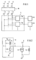
- FIG. 1 merely shows the components of a semiconductor memory which are relevant to the invention and which have individually addressable units 6 which have a multiplicity of memory cells.
- the units 6 can be either bit lines, word lines or memory blocks of the semiconductor memory.
- Other, usually existing components such as drivers and buffers are not shown.
- a programmable address transformation arrangement 10 is shown with inputs 2 and outputs 3, each output 3 being assigned to one of the inputs 2.
- the inputs 2 are each connected to an address connection 1 of the semiconductor memory, to which external address signals 4 can be applied.
- the units 6 can be addressed via an address decoding circuit 5 connected to the outputs 3. If the units are 6 memory blocks, the address decoding circuit 5 is a block decoding circuit. If the units are 6 bit or word lines, the address decoding circuit 5 is a bit address or word address decoding circuit.
- the structure of the address decoding circuit 5 is irrelevant to the invention. It can, for example, be constructed in several stages or perform the address decoding centrally and activate the addressed units 6 directly. As shown in FIG. 1, it can also have a plurality of decentralized address decoders 5a, each of which is assigned to a unit 6 and connected on the one hand to this unit and on the other hand to all outputs 3. Such an implementation exists, for example, when the units 6 are memory blocks and a block decoder in the form of an address decoder 5a is assigned to each of the memory blocks.
- the address transformation arrangement 10 is designed in such a way that, in the unprogrammed state, it passes on external address signals 4, which are present at its inputs 2, as internal address signals 7 to the corresponding outputs 3, so that the address decoding circuit 5, the external addresses present at the address connections 1 in unchanged form also receives as internal addresses. If, as part of a memory test, defective memory cells are found in at least one of the units 6, the number or distribution of which are not acceptable for a desired use of the memory, the transformation arrangement 10 can be programmed in such a way that the outputs 3 are not the ones the address connections 1 present external address is present as an internal address, but a derived, predeterminable other internal address.
- the Address transformation arrangement 10 at at least one of its outputs 3 generates an internal address signal 7 which deviates from the external address signal 4 present at the corresponding input 2.
- the position of a unit 6 with defective memory cells in the logical address space of the semiconductor memory can thus be changed in a targeted manner.
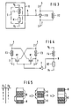
- FIG. 2 shows a part of an exemplary embodiment of the address transformation arrangement 10. For all inputs 2 and associated outputs 3 of the address transformation arrangement 10, arrangements of the same type are provided in this exemplary embodiment.
- An XNOR gate G is shown, the first input of which is one of the inputs 2 of the address transformation arrangement 10 is.
- the output of the XNOR gate G is the associated output 3 of the address transformation arrangement 10.
- a second input of the XNOR gate G is connected to the output A of a recoding unit U.
- the recoding unit U has a series circuit S between a first potential Vx and a second potential Vy of the semiconductor memory.
- the first potential Vx can be, for example, a supply potential applied externally to the semiconductor memory or else an internally generated supply potential.
- the second potential Vy can for example be a reference potential, e.g. B. be mass.
- the series circuit S has a programmable first element F1 which is connected to the first potential Vx and which has a circuit node which forms the output A of the recoding unit U and a resistor R1 which is connected to the first element F1.
- the first element F1 connects the first potential VCC to the output A of the recoding unit U, so that in the XNOR gate G the internal address signal 7 at the output 3 corresponds to the external address signal 4 at the corresponding input 2.
- the first element F1 is programmed, i. H. the connection between the output A of the recoding unit U and the first potential Vx is interrupted, so that essentially the second potential Vy is present at the output A.
- the internal address signal 7 at the output 3 of the XNOR gate G is thus inverse to the external address signal 4 at the input 2.
- the input 2 and the output 3 of the exemplary embodiment in FIG. 2 are additionally connected by an optional, programmable second element F2, which short-circuits the XNOR gate G and thus this part of the address transformation arrangement 10.
- the second element F2 is also a disconnectable connection. In the case where the address transformation arrangement 10 is not programmed, the second element F2 is not separated. In this state, the effect of the gate delay time of the XNOR gate G is suppressed.
- the second element F2 is programmed, that is to say separated, when the first element F1 is programmed, as a result of which its short-circuit effect is canceled.
- the first F1 and second F2 element can be, for example, separation points that can be opened by means of a laser or in an electrical manner. Such separation points are generally referred to as "fuses".
- an inverter ITR with a tri-state output can also be used together with the second element F2 according to FIG. 3, which has a control input S which is connected to the output A of the recoding unit U.
- the first potential Vx is present at the output A of the recoding unit U.
- Output 3 and input 2 of the transformation arrangement 10 are connected via the second element F2. If the internal address signal 7 is now to be inverted with respect to the external address signal 4, the first F1 and the second F2 element are programmed.
- the Tristate inverter ITR then works like an ordinary inverter and its bridging is removed.
- FIG. 4 shows a detail of an exemplary embodiment of the address transformation arrangement 10, in which the assignment of at least two of its outputs 3 to the corresponding inputs 2 is interchanged by the programming.
- Two of the inputs 2 and the two associated outputs 3 are shown, to which they are connected via third programmable elements F3.
- each of the inputs 2 is connected to the output 3 of the other input 2 via the channel path of an n-channel field effect transistor N1.
- the gates of the field effect transistors N1 are connected to one another and to an output of an inverter I.
- An input of the inverter I is connected to a circuit node B between a fourth programmable element F4 and a second resistor R2, which form a series circuit between the first potential Vx and the second potential Vy.
- FIG. 5 shows the method according to the invention using an exemplary embodiment in which the semiconductor memory has four units 6 and a redundant unit 8, which can be addressed by the combination of two external address signals 4, denoted A0 and A1 in the drawing.
- the left part of FIG. 5 shows the external addressing of the units 6 and the redundant unit 8 before the address transformation according to the invention is carried out.
- the redundant unit 8 is initially not activated and no external address is assigned to it.
- the address transformation is carried out by inverting the most significant address signal 4, which is denoted by A 1 in FIG.
- Such an inversion can be carried out, for example, by means of the exemplary embodiments of the address transformation arrangement 10 shown in FIGS. 2 and 3.
- the three parts of FIG. 5 represent the logical address space of the memory. After the transformation has been carried out, the redundant unit 8 with the new external address 00 and the units 6 with the new external addresses 01 and 10 form a coherent, externally addressable memory area without faulty memory cells.
Landscapes
- Engineering & Computer Science (AREA)
- Microelectronics & Electronic Packaging (AREA)
- For Increasing The Reliability Of Semiconductor Memories (AREA)
- Read Only Memory (AREA)
- Techniques For Improving Reliability Of Storages (AREA)
- Static Random-Access Memory (AREA)
Applications Claiming Priority (2)
| Application Number | Priority Date | Filing Date | Title |
|---|---|---|---|
| DE19507312 | 1995-03-02 | ||
| DE19507312A DE19507312C1 (de) | 1995-03-02 | 1995-03-02 | Halbleiterspeicher, dessen Speicherzellen zu einzeln adressierbaren Einheiten zusammengefaßt sind und Verfahren zum Betrieb solcher Speicher |
Publications (2)
| Publication Number | Publication Date |
|---|---|
| EP0730231A2 true EP0730231A2 (fr) | 1996-09-04 |
| EP0730231A3 EP0730231A3 (fr) | 1998-03-04 |
Family
ID=7755458
Family Applications (1)
| Application Number | Title | Priority Date | Filing Date |
|---|---|---|---|
| EP96102690A Withdrawn EP0730231A3 (fr) | 1995-03-02 | 1996-02-22 | Mémoire semi-conductrice avec cellules rassemblée en unité addressable individuellement et méthode d'opération |
Country Status (6)
| Country | Link |
|---|---|
| US (1) | US5671184A (fr) |
| EP (1) | EP0730231A3 (fr) |
| JP (1) | JPH08273389A (fr) |
| KR (1) | KR100314889B1 (fr) |
| DE (1) | DE19507312C1 (fr) |
| TW (1) | TW297897B (fr) |
Families Citing this family (5)
| Publication number | Priority date | Publication date | Assignee | Title |
|---|---|---|---|---|
| US6223248B1 (en) * | 1997-04-29 | 2001-04-24 | Texas Instruments Incorporated | Circuits systems and methods for re-mapping memory row redundancy during two cycle cache access |
| KR100331542B1 (ko) * | 1998-10-09 | 2002-06-20 | 윤종용 | 불량메모리셀어레이블락들을스킵할수있는어드레스디코더를구비하는반도체메모리장치및이를사용하는복합반도체장치 |
| US6542418B2 (en) * | 2001-06-26 | 2003-04-01 | International Business Machines Corporation | Redundant memory array having dual-use repair elements |
| KR101297754B1 (ko) | 2006-07-11 | 2013-08-26 | 삼성전자주식회사 | 메모리 컴파일링 시스템 및 컴파일링 방법 |
| DE202014102153U1 (de) | 2014-05-08 | 2014-05-20 | Astro Engineering Co., Ltd. | Fahrradrahmen mit einem Sicherungssitz |
Family Cites Families (9)
| Publication number | Priority date | Publication date | Assignee | Title |
|---|---|---|---|---|
| NL7415966A (nl) * | 1974-12-09 | 1976-06-11 | Philips Nv | Werkwijze en inrichting voor het opslaan van binaire informatie-elementen. |
| GB2166273A (en) * | 1984-10-29 | 1986-04-30 | Thesys Memory Products Corp | Fault avoidance in semiconductor memories |
| US4649802A (en) * | 1984-10-29 | 1987-03-17 | Allied Corporation | Control valve |
| US5446692A (en) * | 1992-02-14 | 1995-08-29 | Mitsubishi Denki Kabushiki Kaisha | Semiconductor memory device having redundancy memory cells shared among memory blocks |
| DE59310168D1 (de) * | 1993-02-19 | 2001-06-07 | Infineon Technologies Ag | Spalten-Redundanz-Schaltungsanordnung für einen Speicher |
| JP2856645B2 (ja) * | 1993-09-13 | 1999-02-10 | 株式会社東芝 | 半導体記憶装置 |
| KR960008825B1 (en) * | 1993-11-18 | 1996-07-05 | Samsung Electronics Co Ltd | Row redundancy circuit and method of semiconductor memory device with double row decoder |
| DE69320824T2 (de) * | 1993-12-09 | 1999-05-12 | Stmicroelectronics S.R.L., Agrate Brianza, Mailand/Milano | Integrierte Schaltung zur Überwachung der Benutzung von Redunanzspeicherbauelementen in einer Halbleiterspeichereinrichtung |
| JPH07226100A (ja) * | 1994-02-15 | 1995-08-22 | Nec Corp | 半導体メモリ装置 |
-
1995
- 1995-03-02 DE DE19507312A patent/DE19507312C1/de not_active Expired - Lifetime
-
1996
- 1996-02-03 TW TW085101353A patent/TW297897B/zh active
- 1996-02-22 EP EP96102690A patent/EP0730231A3/fr not_active Withdrawn
- 1996-02-29 KR KR1019960005236A patent/KR100314889B1/ko not_active Expired - Fee Related
- 1996-03-01 JP JP8071014A patent/JPH08273389A/ja not_active Withdrawn
- 1996-03-04 US US08/610,047 patent/US5671184A/en not_active Expired - Lifetime
Also Published As
| Publication number | Publication date |
|---|---|
| EP0730231A3 (fr) | 1998-03-04 |
| KR100314889B1 (ko) | 2002-02-28 |
| TW297897B (fr) | 1997-02-11 |
| KR960035642A (ko) | 1996-10-24 |
| DE19507312C1 (de) | 1996-07-25 |
| JPH08273389A (ja) | 1996-10-18 |
| US5671184A (en) | 1997-09-23 |
Similar Documents
| Publication | Publication Date | Title |
|---|---|---|
| DE69128446T2 (de) | Sehr schnelle redundante Zeilen und Spalten für Halbleiter-Speicher | |
| EP0636258B1 (fr) | Memoire a semi-conducteurs integre a redondance | |
| DE3716518C2 (fr) | ||
| DE69019697T2 (de) | Reparierbare Speicherschaltung. | |
| DE3638632C2 (fr) | ||
| DE69023181T2 (de) | Halbleiterspeichergerät mit Redundanz. | |
| DE69520665T2 (de) | Anordnung von nichtflüchtigen EEPROM,insbesondere Flash-EEPROM | |
| DE69330731T2 (de) | Redundanzschaltung für Halbleiterspeichergeräte | |
| DE3886668T2 (de) | Löschbares programmierbares Festwertspeichergerät. | |
| DE3382728T2 (de) | Halbleiteranordnung mit Ersatzspeicherzellen. | |
| DE3520003C2 (fr) | ||
| EP1124232B1 (fr) | Mémoire de semiconducteur intégrée avec l'unité redondante des cellules de mémoire | |
| DE602004001623T2 (de) | TCAM Speicher und Betriebsverfahren | |
| DE3401796A1 (de) | Halbleiterspeichervorrichtung | |
| EP0612074B1 (fr) | Dispositif de colonnes redondantes pour une mémoire | |
| DE3886938T2 (de) | Reprogrammierbare logische Sicherung für logische Anordnungen, basierend auf einer 6-Elementen-SRAM-Zelle. | |
| DE3441473A1 (de) | Halbleiterspeicher | |
| EP0170727B1 (fr) | Mémoire intégrée écriture/lecture | |
| EP0758112A1 (fr) | Dispositif de mémoire à semiconducteur intégrée avec arrangement de circuits redondants | |
| DE102004054968B4 (de) | Verfahren zum Reparieren und zum Betreiben eines Speicherbauelements | |
| EP0224887A1 (fr) | Matrice de portes en technologie CMOS | |
| DE4112891A1 (de) | Halbleiterspeicher mit redundanten bitleitungen | |
| DE19507312C1 (de) | Halbleiterspeicher, dessen Speicherzellen zu einzeln adressierbaren Einheiten zusammengefaßt sind und Verfahren zum Betrieb solcher Speicher | |
| EP1102168B1 (fr) | Mémoire intégrée avec des cellules de mémoire et des cellules de référence | |
| EP0697659B1 (fr) | Circuit de redondance pour une mémoire à circuit intégré à semi-conducteur |
Legal Events
| Date | Code | Title | Description |
|---|---|---|---|
| PUAI | Public reference made under article 153(3) epc to a published international application that has entered the european phase |
Free format text: ORIGINAL CODE: 0009012 |
|
| AK | Designated contracting states |
Kind code of ref document: A2 Designated state(s): AT DE FR GB IE IT NL |
|
| PUAL | Search report despatched |
Free format text: ORIGINAL CODE: 0009013 |
|
| AK | Designated contracting states |
Kind code of ref document: A3 Designated state(s): AT DE FR GB IE IT NL |
|
| 17P | Request for examination filed |
Effective date: 19980819 |
|
| 17Q | First examination report despatched |
Effective date: 20001012 |
|
| RAP1 | Party data changed (applicant data changed or rights of an application transferred) |
Owner name: INFINEON TECHNOLOGIES AG |
|
| GRAG | Despatch of communication of intention to grant |
Free format text: ORIGINAL CODE: EPIDOS AGRA |
|
| GRAG | Despatch of communication of intention to grant |
Free format text: ORIGINAL CODE: EPIDOS AGRA |
|
| GRAH | Despatch of communication of intention to grant a patent |
Free format text: ORIGINAL CODE: EPIDOS IGRA |
|
| GRAH | Despatch of communication of intention to grant a patent |
Free format text: ORIGINAL CODE: EPIDOS IGRA |
|
| STAA | Information on the status of an ep patent application or granted ep patent |
Free format text: STATUS: THE APPLICATION IS DEEMED TO BE WITHDRAWN |
|
| 18D | Application deemed to be withdrawn |
Effective date: 20020903 |
|
| REG | Reference to a national code |
Ref country code: HK Ref legal event code: WD Ref document number: 1003952 Country of ref document: HK |