EP0730295A2 - Halbleitervorrichtung mit gutem thermischem Verhalten - Google Patents
Halbleitervorrichtung mit gutem thermischem Verhalten Download PDFInfo
- Publication number
- EP0730295A2 EP0730295A2 EP96102018A EP96102018A EP0730295A2 EP 0730295 A2 EP0730295 A2 EP 0730295A2 EP 96102018 A EP96102018 A EP 96102018A EP 96102018 A EP96102018 A EP 96102018A EP 0730295 A2 EP0730295 A2 EP 0730295A2
- Authority
- EP
- European Patent Office
- Prior art keywords
- island
- chip
- opening
- semiconductor chip
- system carrier
- Prior art date
- Legal status (The legal status is an assumption and is not a legal conclusion. Google has not performed a legal analysis and makes no representation as to the accuracy of the status listed.)
- Granted
Links
Images


Classifications
-
- H—ELECTRICITY
- H10—SEMICONDUCTOR DEVICES; ELECTRIC SOLID-STATE DEVICES NOT OTHERWISE PROVIDED FOR
- H10W—GENERIC PACKAGES, INTERCONNECTIONS, CONNECTORS OR OTHER CONSTRUCTIONAL DETAILS OF DEVICES COVERED BY CLASS H10
- H10W70/00—Package substrates; Interposers; Redistribution layers [RDL]
- H10W70/40—Leadframes
- H10W70/411—Chip-supporting parts, e.g. die pads
-
- H—ELECTRICITY
- H10—SEMICONDUCTOR DEVICES; ELECTRIC SOLID-STATE DEVICES NOT OTHERWISE PROVIDED FOR
- H10W—GENERIC PACKAGES, INTERCONNECTIONS, CONNECTORS OR OTHER CONSTRUCTIONAL DETAILS OF DEVICES COVERED BY CLASS H10
- H10W72/00—Interconnections or connectors in packages
- H10W72/071—Connecting or disconnecting
- H10W72/073—Connecting or disconnecting of die-attach connectors
-
- H—ELECTRICITY
- H10—SEMICONDUCTOR DEVICES; ELECTRIC SOLID-STATE DEVICES NOT OTHERWISE PROVIDED FOR
- H10W—GENERIC PACKAGES, INTERCONNECTIONS, CONNECTORS OR OTHER CONSTRUCTIONAL DETAILS OF DEVICES COVERED BY CLASS H10
- H10W72/00—Interconnections or connectors in packages
- H10W72/50—Bond wires
- H10W72/531—Shapes of wire connectors
- H10W72/5363—Shapes of wire connectors the connected ends being wedge-shaped
-
- H—ELECTRICITY
- H10—SEMICONDUCTOR DEVICES; ELECTRIC SOLID-STATE DEVICES NOT OTHERWISE PROVIDED FOR
- H10W—GENERIC PACKAGES, INTERCONNECTIONS, CONNECTORS OR OTHER CONSTRUCTIONAL DETAILS OF DEVICES COVERED BY CLASS H10
- H10W72/00—Interconnections or connectors in packages
- H10W72/851—Dispositions of multiple connectors or interconnections
- H10W72/874—On different surfaces
- H10W72/884—Die-attach connectors and bond wires
-
- H—ELECTRICITY
- H10—SEMICONDUCTOR DEVICES; ELECTRIC SOLID-STATE DEVICES NOT OTHERWISE PROVIDED FOR
- H10W—GENERIC PACKAGES, INTERCONNECTIONS, CONNECTORS OR OTHER CONSTRUCTIONAL DETAILS OF DEVICES COVERED BY CLASS H10
- H10W74/00—Encapsulations, e.g. protective coatings
-
- H—ELECTRICITY
- H10—SEMICONDUCTOR DEVICES; ELECTRIC SOLID-STATE DEVICES NOT OTHERWISE PROVIDED FOR
- H10W—GENERIC PACKAGES, INTERCONNECTIONS, CONNECTORS OR OTHER CONSTRUCTIONAL DETAILS OF DEVICES COVERED BY CLASS H10
- H10W90/00—Package configurations
- H10W90/701—Package configurations characterised by the relative positions of pads or connectors relative to package parts
- H10W90/731—Package configurations characterised by the relative positions of pads or connectors relative to package parts of die-attach connectors
- H10W90/736—Package configurations characterised by the relative positions of pads or connectors relative to package parts of die-attach connectors between a chip and a stacked lead frame, conducting package substrate or heat sink
-
- H—ELECTRICITY
- H10—SEMICONDUCTOR DEVICES; ELECTRIC SOLID-STATE DEVICES NOT OTHERWISE PROVIDED FOR
- H10W—GENERIC PACKAGES, INTERCONNECTIONS, CONNECTORS OR OTHER CONSTRUCTIONAL DETAILS OF DEVICES COVERED BY CLASS H10
- H10W90/00—Package configurations
- H10W90/701—Package configurations characterised by the relative positions of pads or connectors relative to package parts
- H10W90/751—Package configurations characterised by the relative positions of pads or connectors relative to package parts of bond wires
- H10W90/756—Package configurations characterised by the relative positions of pads or connectors relative to package parts of bond wires between a chip and a stacked lead frame, conducting package substrate or heat sink
Definitions
- the invention relates to a semiconductor device with a semiconductor chip and a system carrier connected thereto, the island of which has an opening.
- the semiconductor chip is first connected to a system carrier.
- This system carrier consists of a frame in which an island-shaped chip carrier and connections for the finished product are usually provided.
- the connection of the semiconductor chip with the system carrier, ie with the island carrying the chip, is typically done by gluing or an alloy.
- After mounting the semiconductor chip its individual connection points with the connections of the carrier frame z. B. connected with bond wires.
- the semiconductor chip and the connections of the lead frame are then encapsulated in such a way that the semiconductor chip is completely encapsulated and the connections of the housing are electrically and mechanically accessible.
- the parts of the lead frame that are not required are then removed by punching.
- the housing usually consists of a hardening plastic molding compound.
- Standardized plastic housings are getting thinner and thinner.
- the TSOP design thin small outline package
- the chips built into the housing become larger.
- housing designs up to 20 x 20 mm 2 are provided (TQFP - thin quad flat package).
- the stabilizing effect of the plastic covering is reduced. Since the connection of the chip to the island and the encapsulation with molding compound takes place at temperatures of at least 180 ° C., play a role in semiconductor devices With large lateral dimensions and extremely thin housings, the thermal expansion coefficients of the materials involved play an important role. Ideally, all expansion coefficients should be of the same size so that no bimetal effect can occur when the device cools down and the chip system carrier island assembly cannot bend.
- the coefficients of expansion of the main materials vary widely. Silicon has a coefficient of thermal expansion of 3, the molding mass of the housing of approximately 17 and a typical island material such as copper also of approximately 17, each in units of ppm / K. A maximum of 30 ⁇ m is considered acceptable as the permissible housing bending in order to ensure the coplanarity of these connections of the finished component during further processing, i.e. ensure when soldering.
- thermomechanical system carrier islands which are better adapted to silicon, for example NiFe alloys, as are known from DE-A-42 31 705.
- the heat dissipation and thus the thermal conductivity of the NeFe alloys is 10 to 20 times worse than that of copper alloys.
- the thermal resistance of a component does not increase when changing the leedframe material from copper to nickel-iron alloys in accordance with the differences in the thermal conductivity numbers.
- higher chip temperatures reduce the reliability and service life of the entire component.
- special housings with an inserted heat distributor (heat slug) or with heat sinks are necessary, which is expensive and complicated to manufacture.
- the invention is therefore based on the object of specifying a semiconductor device with a composite of a semiconductor chip and a system carrier island, which is improved both in terms of the thermomechanical and also the heat dissipation behavior.
- the invention is based on the finding that, in the case of large chips, the island is only of comparatively little importance for heat dissipation, but that the chip carrier island cannot be reduced arbitrarily, since otherwise unstable conditions form when the chip is mounted on the system carrier. In particular, tilting of the chip can lead to a lack of planarity in the chip system carrier assembly.
- the invention enables a safe, flat assembly of the chip on the island with good heat dissipation, even for small chips in which the system carrier island plays an important role in heat dissipation, and a low degree of housing deflection in the finished product.
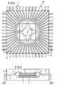
- a semiconductor chip 1 with the edges 11 is freely connected to a system carrier island with the aid of a connection 2, for example an adhesive.
- the chip 1 is electrically connected with the aid of bonding wires 4 to connections 5, which are freely accessible after the overmolding of the arrangement with a molding compound 6 for further processing of the device.
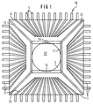
- FIG. 1 shows a schematic plan view of a section through an arrangement 10, according to FIG. 5 approximately at the level of the chip carrier island 3, the edges 11 of the chip 3 and the connections 5 being also shown.
- the chip carrier island 3 is fastened to narrow diagonal carriers 12, with which the chip carrier island was fastened to the latter before the parts of the lead frame which were no longer required were punched out.
- the chip carrier island 3 has a large-area central opening 13 which projects beyond the edge of the chip on two sides of the chip. Since in the exemplary embodiment the opening is approximately circular and the chip is rectangular, the diameter of the opening is larger than the shorter side of the calf conductor chip. 1 shows an opening with a diameter which corresponds approximately to the length of the long side of the chip.
- the web region 15 of the system carrier island 3, which is outlined in dashed lines, remains without any contact with the chip.
- the chip carrier island 21 is fastened to outer strips 22 and has a rectangular opening 23 which is rotated relative to the semiconductor chip with an edge 11 such that the corners 24 of the opening protrude beyond the long sides of the chip opening.
- the opening on all long sides of the semiconductor chip is wider than the semiconductor chip.
- the outer border of the chip carrier island 31 is octagonal.
- the opening 33 is approximately rectangular and, similar to FIG. 2, is rotated relative to the chip in such a way that the corners 34 of the opening lie on the long sides of the chip edge 11. In this case too, web-shaped regions 35 remain on the long sides of the semiconductor chip, which do not touch the latter.
- additional openings 36 are provided on two long sides of the chip in the remaining web area of the system carrier 31, which openings are delimited by two narrow webs 37 and 38 and by two further areas of the system carrier.
- the webs 37 and 38 are angled, in the exemplary embodiment in the direction of the semiconductor chip, so that the elements 36 to 38 result in an expansion area for the chip carrier island when the chip extends transversely to the two opposite expansion areas.
- FIG. 4 shows a further arrangement 40, in which the opening 43 of the system carrier island 41 is designed in the manner of a cross, the opening tips of which point in the direction of the long sides of the semiconductor chip.
- This embodiment is particularly suitable for use even with small chips, the minimal size of which is indicated by the dashed line 44.
- the arrangement has the advantage that, compared to the exemplary embodiments in FIGS. 1-3, even smaller chip sizes can be used. In a device according to the invention, only one system carrier or one system carrier island can be used for a large number of different chip sizes.
- a copper alloy is preferably used as the material for the leadframe or for the system carrier island.
- the system carrier island is designed so that as little island material as possible remains through the opening under the mounted chip.
- the opening can be punched out or etched.
- the device according to the invention is characterized in that the semiconductor chip no longer rests on the system carrier or is connected to the system carrier only in the region of its corners and possibly in the narrowest possible edge region. As a result, expansion areas can be provided outside the chip area in the system carrier island, the expansion of which has no effect on the expansion of the chip.
- the web areas lying outside the chip border can in principle also be completely omitted, so that the four connection areas of the system carrier island with the chip are completely separated from one another at the corners thereof.
- a prerequisite is sufficient mechanical stability of the island parts. This is particularly the case when connections remain connected directly to the island parts and therefore, in addition to the island suspension, there is additional stabilization of the island areas. In this case it is possible to separate the corner areas of the system carrier island before the die bonding.
- the expansion areas 36 to 38 shown in FIG. 3 can be designed such that they tear as a predetermined breaking point when the termomechanical load is weak, so that individual areas, in particular the four corner areas of the system carrier island, are completely separated from one another.
- the embodiment shown in FIG. 3 and FIG. 4 with an octagonal basic shape of the system carrier island has the particular advantage that it follows the mostly obliquely recessed connections 5 at a minimum distance and the poorly heat-conducting plastic zone 6 between the island edge and the connection tips is as thin as possible is held.
- the device according to the invention has the further advantage that the thermomechanical tensile forces of the island which occur during cooling are reduced compared to the chip and long straight lines of action of the tensile forces are shortened or even shortened to be interrupted. In particular over the long chip diagonals and as far as possible also along the chip edges, a continuous build-up of force is prevented by the device according to the invention. It goes without saying that the invention is not limited to the embodiments shown in exemplary embodiments, in particular not to PQFP designs, but can also be applied to other plastic designs.
- the material used is not a nickel-iron alloy but a copper alloy. This allows a significantly improved heat dissipation to be achieved without enlarging or even reducing the thermomechanical bending of the semiconductor device, without a heat distributor or a heat-conducting plate being inserted into the housing or without a heat sink having to be attached to the housing.
- the invention has the advantage that the chip can be attached to the system carrier in a stable manner and at the same time a system carrier can be used for a plurality of different chip sizes.
Landscapes
- Lead Frames For Integrated Circuits (AREA)
- Cooling Or The Like Of Semiconductors Or Solid State Devices (AREA)
- Internal Circuitry In Semiconductor Integrated Circuit Devices (AREA)
Abstract
Description
- Die Erfindung betrifft eine Halbleitervorrichtung mit einem Halbleiterchip und einem damit verbundenen Systemträger, dessen Insel eine Öffnung aufweist.
- Halbleiterchips werden zum Schutz vor Zerstörung und Umwelteinflussen sowie zur besseren Handhabbarkeit im Gehäuse montiert. Bevorzugte Bauform für Massenprodukte ist das Plastikgehäuse. Dabei wird der Halbleiterchips zunächst mit einem Systemträger verbunden. Dieser Systemträger besteht aus einem Rahmen, in den üblicherweise ein inselförmiger Chipträger sowie Anschlüsse für das fertige Produkt vorgesehen sind. Die Verbindung des Halbleiterchips
mit dem Systemträger, d.h. mit der den Chip tragenden Insel, erfolgt typischerweise durch eine Klebung oder eine Legierung. Nach der Montage des Halbleiterchips werden dessen einzelne Anschlußpunkte mit den Anschlüssen des Trägerrahmens z. B. mit Bonddrähten verbunden. Danach werden der Halbleiterchip und die Anschlüsse des Anschlußrahmens so umspritzt, daß der Halbleiterchip vollständig gekapselt ist und die Anschlüsse des Gehäuses elektrisch und mechanisch zugänglich sind. Die nicht benötigten Teile des Anschlußrahmens (lead frame) werden danach durch Stanzen entfernt. Das Gehäuse besteht üblicherweise aus einer härtenden Kunststoff-Preßmasse. - Standardisierte Plastikgehäuse werden immer dünner. Die derzeit bereits eingesetzte TSOP-Bauform (thin small outline package) hat noch eine Gehäusedicke von 1 mm. Gleichzeitig werden die in die Gehäuse eingebauten Chips größer. Bei Chipabmessungen von größer 10 x 10 mm2 sind Gehäusebauformen bis 20 x 20 mm2 vorgesehen (TQFP - thin quad flat package). Bei dünnen Plastikgehäusen ist ein Stabilisierungseffekt der Plastikumhüllung reduziert. Da die Verbindung des Chips mit der Insel und das Umspritzen mit Preßmasse bei Temperaturen von mindestens 180°C erfolgt, spielen deshalb bei Halbleitervorrichtungen mit großen lateralen Abmessungen und extrem dünnen Gehäusen die thermischen Ausdehnungskoeffizienten der beteiligten Materialien eine wesentliche Rolle. Idealerweise müßten alle Ausdehnungskoeffizienten gleich groß sein, damit beim Abkühlen der Vorrichtung kein Bimetalleffekt auftreten kann und sich der Chip-Systemträgerinsel-Verbund nicht verbiegen kann.
- Tatsächlich sind jedoch die Ausdehnungskoeffizienten der Hauptmaterialien stark unterschiedlich. Silizium hat einen thermischen Ausdehnungskoeffizienten von 3, die Preßmasse des Gehäuses von etwa 17 und ein typisches Inselmaterial wie Kupfer ebenfalls von etwa 17, jeweils in Einheiten ppm/K. Als zulässige Gehäuseverbiegung werden maximal 30 µm als akzeptabel angesehen, um die Koplanarität dieser Anschlüsse des fertigen Bauelements bei der Weiterverarbeitung, d.h. beim Löten sicherzustellen.
- Eine Möglichkeit zur Verbesserung des Durchbiegeverhaltens besteht in der Verwendung von thermomechanischen besser an Silizium angepaßte Systemträgerinseln, beispielsweise NiFe-Legierungen, wie sie aus der DE-A-42 31 705 bekannt sind. Dem stehen jedoch die zunehmenden Integrationsdichten und Taktraten der Chips entgegen, die zu höheren Verlustleistungen fuhren. Die Wärmeabfuhr und damit die Wärmeleitfähigkeit der NeFe-Legierungen ist 10 bis 20 mal schlechter als bei Kupfer-Legierungen. Zwar vergrößert sich der Wärmewiderstand eines Bauelements beim Wechsel des Leedframematerials von Kupferauf Nickel-Eisen-Legierungen nicht entsprechend der Unterschiede in den Wärmeleitfähigkeitszahlen. Selbst wenn jedoch kritische Temperaturen nicht überschritten werden, verringern höhere Chiptemperaturen die Zuverlässigkeit und Lebensdauer des gesamten Bauelements. Für die Wärmeabfuhr von Schaltungen mit hoher Verlustleistung sind dann spezielle Gehäuse mit eingelegtem Wärmeverteiler (heat slug) oder mit Kühlkörpern notwendig, was teuer und kompliziert herzustellen ist.
- Aus den US-A-4,952,999 und US-A-5,150,193 sind Systemträgerinseln mit Schlitzen bekannt. Das letztere Dokument zeigt außerdem einen Systemträger mit einer zentralen Öffnung, deren Durchmesser jedoch kleiner als die lateralen Chipabmessungen sind und deren Fläche erheblich kleiner als die Chipfläche ist. Beide Möglichkeiten führen zu unakzeptablen Gehäusedurchbiegungen.
- Der Erfindung liegt deshalb die Aufgabe zugrunde, eine Halbleitervorrichtung mit einem Verbund aus einem Halbleiterchip und einer Systemträgerinsel anzugeben, die sowohl hinsichtlich des termomechanischen als auch des Wärmeabfuhrverhaltens verbessert ist.
- Diese Aufgabe wird durch die Merkmale der Patentansprüche 1 und 9 gelöst.
- Der Erfindung liegt die Erkenntnis zugrunde, daß bei großen Chips die Insel für die Wärmeabfuhr nur eine geringe vergleichsweise Bedeutung hat, daß jedoch die Chipträgerinsel nicht beliebig verkleinert werden kann, da sich ansonsten bei der Montage des Chips auf dem Systemträger unstabile Verhältnisse bilden. Insbesondere kann eine Verkantung des Chips zu fehlender Planarität des Chip-Systemträger-Verbundes führen. Die Erfindung ermöglicht eine sichere plane Montage des Chips auf der Insel mit einer guten Wärmeabfuhr auch für kleine Chips, bei denen die Systemträgerinsel eine bedeutende Rolle für die Wärmeabfuhr spiel, und eine geringe Gehäusedurchbiegung des fertigen Produkts.
- Ausbildungen der Erfindung sind in Unteransprüchen gekennzeichnet. Die Erfindung wird nachfolgend anhand von Ausführungsbeispielen näher beschrieben. Es zeigen:
- FIG 1 bis 4 schematische Darstellungen eines Systemträgers mit einem für den zu montierenden Chip vorgesehenen Bereich,
- FIG 5 einen Querschnitt durch ein Bauelement zur Verdeutlichung der Erfindung.
- Gemäß FIG 5 ist ein Halbleiterchip 1 mit den Rändern 11 mit Hilfe einer Verbindung 2, beispielsweise eines Klebstoffes, mit einer Systemträgerinsel frei verbunden. Der Chip 1 wird mit Hilfe von Bonddrähten 4 elektrisch mit Anschlüssen 5 verbunden, die nach dem Umspritzen der Anordnung mit einer Preßmasse 6 zur Weiterverarbeitung der Vorrichtung frei zugänglich sind.
- FIG 1 zeigt eine schematische Draufsicht auf einen Schnitt durch eine Anordnung 10, gemäß FIG 5 etwa in Höhe der Chipträgerinsel 3, wobei die Ränder 11 des Chips 3 sowie die Anschlüsse 5 mit eingezeichnet sind. Die Chipträgerinsel 3 ist an schmalen Diagonalträgern 12 befestigt, mit denen die Chipträgerinsel vor dem Ausstanzen der nicht mehr benötigten Teile des Leiterrahmens an letzterem befestigt war. Die Chipträgerinsel 3 hat eine großflächige zentrale Öffnung 13, die an zwei Seiten des Chips über den Chiprand hinausragt. Da im Ausführungsbeispiel die Öffnung etwa kreisförmig und der Chip rechtwinklig ausgebildet ist, ist der Durchmesser der Öffnung größer als die kürzere Seite des Kalbleiterchips. FIG 1 zeigt eine Öffnung mit einem Durchmesser, der etwa der Länge der Längsseite des Chips entspricht. Es ist jedoch auch möglich, den Durchmesser etwas kleiner oder etwas größer als die Längsseite des Chips zu wählen. Im letzteren Fall wäre die Öffnung an allen Seiten des Chips breiter als dieser. Im Ausführungsbeispiel bleibt der gestrichelt umrandete Stegbereich 15 der Systemträgerinsel 3 ohne jeden Kontakt zum Chip.
- In der Anordnung 20 nach FIG 2 ist die Chipträgerinsel 21 an äußeren Streifen 22 befestigt und hat eine rechteckförmige Öffnung 23, die so gegenüber dem Halbleiterchip mit einem Rand 11 gedreht ist, daß die Ecken 24 der Öffnung über die Längsseiten der Chipöffnung hinausragen. In diesem Fall ist die Öffnung an allen Längsseiten des Halbleiterchips breiter als der Halbleiterchip. Es verbleiben stegförmige Bereiche 25, die an den Längsseiten des Halbleiterchips nicht vom Chip abgedeckt sind.
- In der Anordnung 30 gemäß FIG 3 ist die äußere Umrandung der Chipträgerinsel 31 achteckig. Die Öffnung 33 ist dagegen etwa rechteckförmig und ähnlich wie bei FIG 2 gegenüber dem Chip so gedreht, daß die Ecken 34 der Öffnung an den Längsseiten des Chiprandes 11 liegen. Auch in diesem Fall verbleiben stegförmige Bereiche 35 an den Längsseiten des Halbleiterchips, die diesen nicht berühren. In FIG 3 sind an zwei Längsseiten des Chips im verbleibenden Stegbereich des Systemträgers 31 zusätzliche Öffnungen 36 vorgesehen, die von zwei schmalen Stegen 37 und 38 sowie von weiteren zwei Bereichen des Systemträgers begrenzt sind. Die Stege 37 und 38 sind abgewinkelt, im Ausführungsbeispiel in Richtung auf den Halbleiterchip, so daß sich durch die Elemente 36 bis 38 ein Dehnungsbereich für die Chipträgerinsel ergibt, wenn sich der Chip quer zu den beiden gegenüberliegenden Dehnungsbereichen ausdehnt.
- FIG 4 zeigt eine weitere Anordnung 40, bei der die Öffnung 43 der Systemträgerinsel 41 in Art eines Kreuzes ausgebildet ist, dessen Öffnungsspitzen in Richtung der Langsseiten des Halbleiterchips zeigen. Diese Ausführungsform eignet sich besonders zur Verwendung auch mit kleinen Chips, dessen etwa minimale Größe durch die gestrichelte Linie 44 angedeutet ist. Die Anordnung hat den Vorteil, daß im Vergleich zu den Ausführungsbeispielen der Figuren 1 - 3 noch kleinere Chipgrößen verwendet werden können. Bei einer erfindungsgemäßen Vorrichtung kann lediglich ein Systemträger bzw. eine Systemträgerinsel für eine Vielzahl unterschiedlicher Chipgrößen verwendet werden.
- Bevorzugt wird als Material für den leadframe bzw. für die Systemträgerinsel eine Kupferlegierung verwendet. Die Systemträgerinsel ist so ausgebildet, daß durch die Öffnung unter dem montierten Chip möglichst wenig Inselmaterial verbleibt. Die Öffnung kann ausgestanzt oder geätzt werden. Die erfin dungsgemäße Vorrichtung zeichnet sich dadurch aus, daß der Halbleiterchip nicht mehr vollflächig, sondern nur noch im Bereich seiner Ecken und eventuell in einem möglichst schmalen Randbereich auf dem Systemträger aufliegt bzw. mit diesem verbunden ist. Dadurch können außerhalb des Chipbereichs in der Systemträgerinsel Dehnungsbereiche vorgesehen werden, deren Dehnung keine Rückwirkung auf die Dehnung des Chips hat.
- Die außerhalb der Chipumrandung liegenden Stegbereiche können grundsätzlich auch vollständig entfallen, so daß die vier Verbindungsbereiche der Systemträgerinsel mit dem Chip an dessen Ecken vollständig voneinander getrennt sind. Voraussetzung ist eine hinreichende mechanische Stabilität der Inselteile. Dies ist insbesondere dann gegeben, wenn Anschlüsse direkt mit den Inselteilen verbunden bleiben und deshalb neben der Inselaufhängung zusätzlich eine Stabilisierung der Inselbereiche gegeben ist. Es ist in diesem Fall möglich, die Eckbereiche der Systemträgerinsel bereits vor dem Die-Bonden aufzutrennen.
- Die in FIG 3 gezeigten Dehnungsbereiche 36 bis 38 können so ausgelegt sein, daß sie bei schwacher termomechanischer Belastung als Sollbruchstelle reißen, so daß einzelne Bereiche, insbesondere die vier Eckbereiche der Systemträgerinsel vollständig voneinander getrennt sind. Die in FIG 3 und FIG 4 gezeigte Ausführungsform mit einer 8-eckigen Grundform der Systemträgerinsel hat den besonderen Vorteil, daß sie den meist schräg zurückgesetzten Anschlüssen 5 in minimalem Abstand folgt und die schlecht wärmeleitende Plastikzone 6 zwischen dem Inselrand und den Anschlußspitzen so dünn wie möglich gehalten wird.
- Die erfindungsgemäße Vorrichtung hat den weiteren Vorteil, daß die beim Abkühlen auftretenden thermomechanischen Zugkräfte der Insel gegenüber dem Chip verringert und lange gerade Wirkungslinien der Zugkräfte verkürzt oder sogar unterbrochen werden. Insbesondere über die langen Chipdiagonalen und möglichst weitgehend auch entlang der Chipränder wird durch die erfindungsgemäße Vorrichtung ein durchgängiger Kraftaufbau verhindert. Es versteht sich von selbst, daß die Erfindung nicht auf die in Ausführungsbeispielen gezeigten Ausführungsformen, insbesondere nicht auf PQFP-Bauformen beschränkt ist, sondern sich auch auf andere Plastikbauformen übertragen läßt.
- Der entscheidende Vorteil der Erfindung gegenüber bisher bekannten Anordnungen besteht darin, daß als Systemträger Material keine Nickel-Eisen-Legierung, sondern eine Kupfer-Legierung verwendet werden kann. Dadurch läßt sich ohne Vergrößerung oder sogar mit einer Verringerung der thermomechanischen Biegung der Halbleitervorrichtung eine erheblich verbesserte Wärmeableitung erreichen, ohne daß ein Wärmeverteiler oder eine Wärmeleitplatte in das Gehäuse eingelegt werden oder ohne daß ein Kühlkörper am Gehäuse angebracht werden muß. Schließlich hat die Erfindung den Vorteil, daß sich der Chip in stabiler Weise auf dem Systemträger befestigen läßt und gleichzeitig ein Systemträger für eine Mehrzahl von unterschiedlichen Chipgrößen verwendet werden kann.
Claims (10)
- Halbleitervorrichtung mit einem Halbleiterchip und einem damit verbundenen Systemträger, dessen Insel eine Öffnung aufweist,
dadurch gekennzeichnet,
daß die Öffnung (13, 23, 33, 43) großflächig zentral angeordnet und an zwei Längsseiten des Halbleiterchips (1) breiter als der Halbleiterchip ist. - Vorrichtung nach Anspruch 1,
dadurch gekennzeichnet,
daß die Öffnung an jeder Längsseite breiter als der zugeordnete Rand des Halbleiterchips ist. - Vorrichtung nach Anspruch 1 oder 2,
dadurch gekennzeichnet,
daß die Insel (3, 21, 31, 41) im Bereich der über den Chiprand hinausragenden Öffnung als Dehnungsbereich (36 bis 38) ausgebildet ist. - Vorrichtung nach einem der vorhergehenden Ansprüche,
dadurch gekennzeichnet,
daß die Insel (3, 21, 31, 41) im Bereich der über den Chiprand hinausragenden Öffnung aufgetrennt ist. - Vorrichtung nach einem der vorhergehenden Ansprüche,
dadurch gekennzeichnet,
daß die Außenränder der Insel in ihrer Form an die Form der Anschlüsse (5) der Halbleitervorrichtung angebracht sind. - Vorrichtung nach einem der vorhergehenden Ansprüche,
gekennzeichnet durch eine zentrale gerundete Öffnung der Insel. - Vorrichtung nach einem der Ansprüche 1 bis 5,
gekennzeichnet durch eine rautenförmige Öffnung in der Insel. - Vorrichtung nach einem der Ansprüche 1 bis 5,
gekennzeichnet durch eine zentrale kreuzförmige oder sternförmige Öffnung in der Insel. - Halbleitervorrichtung mit einem Halbleiterchip und mit einem damit verbundenen Systemträger, dessen Insel eine Öffnung aufweist,
dadurch gekennzeichnet,
daß der Halbleiterchip (1) allein in seinen Eckbereichen mit der Insel (3, 21, 32, 41) verbunden ist. - Vorrichtung nach einem der Ansprüche 1 bis 9,
durch gekennzeichnet,
daß die Insel aus Kupfer oder einer Kupferlegierung besteht.
Applications Claiming Priority (2)
| Application Number | Priority Date | Filing Date | Title |
|---|---|---|---|
| DE19506958 | 1995-02-28 | ||
| DE19506958A DE19506958C2 (de) | 1995-02-28 | 1995-02-28 | Halbleitervorrichtung mit gutem thermischen Verhalten |
Publications (3)
| Publication Number | Publication Date |
|---|---|
| EP0730295A2 true EP0730295A2 (de) | 1996-09-04 |
| EP0730295A3 EP0730295A3 (de) | 1999-04-28 |
| EP0730295B1 EP0730295B1 (de) | 2008-04-02 |
Family
ID=7755245
Family Applications (1)
| Application Number | Title | Priority Date | Filing Date |
|---|---|---|---|
| EP96102018A Expired - Lifetime EP0730295B1 (de) | 1995-02-28 | 1996-02-12 | Halbleitervorrichtung mit gutem thermischem Verhalten |
Country Status (4)
| Country | Link |
|---|---|
| US (1) | US5982028A (de) |
| EP (1) | EP0730295B1 (de) |
| AT (1) | ATE391342T1 (de) |
| DE (2) | DE19506958C2 (de) |
Cited By (1)
| Publication number | Priority date | Publication date | Assignee | Title |
|---|---|---|---|---|
| DE19639181A1 (de) * | 1996-09-24 | 1998-04-02 | Siemens Ag | Zuleitungsrahmen für ein mikroelektronisches Bauelement |
Families Citing this family (3)
| Publication number | Priority date | Publication date | Assignee | Title |
|---|---|---|---|---|
| US6118599A (en) * | 1998-11-03 | 2000-09-12 | Nikon Corporation | Hybrid optical barrel |
| JP2000349221A (ja) * | 1999-06-02 | 2000-12-15 | Sharp Corp | リードフレームおよびそれを用いた半導体デバイス |
| DE102006037538B4 (de) * | 2006-08-10 | 2016-03-10 | Infineon Technologies Ag | Elektronisches Bauteil, elektronischer Bauteilstapel und Verfahren zu deren Herstellung sowie Verwendung einer Kügelchenplatziermaschine zur Durchführung eines Verfahrens zum Herstellen eines elektronischen Bauteils bzw. Bauteilstapels |
Family Cites Families (22)
| Publication number | Priority date | Publication date | Assignee | Title |
|---|---|---|---|---|
| JPS57133655A (en) * | 1981-02-10 | 1982-08-18 | Pioneer Electronic Corp | Lead frame |
| JPS5961055A (ja) * | 1982-09-29 | 1984-04-07 | Toshiba Corp | 半導体装置 |
| JPS59201451A (ja) * | 1983-04-28 | 1984-11-15 | Rohm Co Ltd | リ−ドフレ−ム |
| JPS6068639A (ja) * | 1983-08-31 | 1985-04-19 | Toshiba Corp | 樹脂封止型半導体装置 |
| JPS63169753A (ja) * | 1987-01-07 | 1988-07-13 | Nec Yamagata Ltd | リ−ドフレ−ム |
| JPH0680760B2 (ja) * | 1987-03-13 | 1994-10-12 | 株式会社日立製作所 | リ−ドフレ−ム並びに半導体装置 |
| US5150193A (en) * | 1987-05-27 | 1992-09-22 | Hitachi, Ltd. | Resin-encapsulated semiconductor device having a particular mounting structure |
| JPS6480051A (en) * | 1987-09-21 | 1989-03-24 | Hitachi Ltd | Electric device |
| US4952999A (en) * | 1988-04-26 | 1990-08-28 | National Semiconductor Corporation | Method and apparatus for reducing die stress |
| JPH0294463A (ja) * | 1988-09-29 | 1990-04-05 | Matsushita Electron Corp | 半導体装置 |
| US5021864A (en) * | 1989-09-05 | 1991-06-04 | Micron Technology, Inc. | Die-mounting paddle for mechanical stress reduction in plastic IC packages |
| JPH03283648A (ja) * | 1990-03-30 | 1991-12-13 | Nec Corp | 樹脂封止型半導体装置 |
| JPH0415947A (ja) * | 1990-05-09 | 1992-01-21 | Hitachi Cable Ltd | 半導体装置用リードフレームおよび半導体装置 |
| JPH05102389A (ja) * | 1991-10-09 | 1993-04-23 | Hitachi Ltd | メモリーic部品 |
| EP0566872A3 (en) * | 1992-04-21 | 1994-05-11 | Motorola Inc | A thermally enhanced semiconductor device and method for making the same |
| JPH0629445A (ja) * | 1992-07-07 | 1994-02-04 | Fujitsu Ltd | リードフレーム及び半導体装置 |
| US5233222A (en) * | 1992-07-27 | 1993-08-03 | Motorola, Inc. | Semiconductor device having window-frame flag with tapered edge in opening |
| JPH0685145A (ja) * | 1992-09-02 | 1994-03-25 | Toshiba Corp | 半導体装置 |
| JPH0685151A (ja) * | 1992-09-02 | 1994-03-25 | Seiko Epson Corp | 半導体装置とその製造方法 |
| DE4231705C2 (de) * | 1992-09-22 | 1998-04-30 | Siemens Ag | Halbleitervorrichtung mit einem Systemträger und einem damit verbundenen Halbleiterchip sowie Verfahren zu deren Herstellung |
| JPH06268146A (ja) * | 1993-03-15 | 1994-09-22 | Toshiba Corp | 半導体装置 |
| US5336639A (en) * | 1993-06-28 | 1994-08-09 | Motorola, Inc. | Method for securing a semiconductor chip to a leadframe |
-
1995
- 1995-02-28 DE DE19506958A patent/DE19506958C2/de not_active Expired - Lifetime
-
1996
- 1996-02-12 DE DE59611466T patent/DE59611466D1/de not_active Expired - Lifetime
- 1996-02-12 AT AT96102018T patent/ATE391342T1/de not_active IP Right Cessation
- 1996-02-12 EP EP96102018A patent/EP0730295B1/de not_active Expired - Lifetime
- 1996-02-28 US US08/608,491 patent/US5982028A/en not_active Expired - Lifetime
Cited By (2)
| Publication number | Priority date | Publication date | Assignee | Title |
|---|---|---|---|---|
| DE19639181A1 (de) * | 1996-09-24 | 1998-04-02 | Siemens Ag | Zuleitungsrahmen für ein mikroelektronisches Bauelement |
| DE19639181B4 (de) * | 1996-09-24 | 2006-08-17 | Infineon Technologies Ag | Mikroelektronisches Bauelement mit einem Zuleitungsrahmen und einem integrierten Schaltkreis |
Also Published As
| Publication number | Publication date |
|---|---|
| EP0730295B1 (de) | 2008-04-02 |
| DE19506958C2 (de) | 1998-09-24 |
| ATE391342T1 (de) | 2008-04-15 |
| EP0730295A3 (de) | 1999-04-28 |
| DE59611466D1 (de) | 2008-05-15 |
| US5982028A (en) | 1999-11-09 |
| DE19506958A1 (de) | 1996-08-29 |
Similar Documents
| Publication | Publication Date | Title |
|---|---|---|
| DE69131712T2 (de) | Lottragender anschlussdraht | |
| DE69637488T2 (de) | Halbleiter und Halbleitermodul | |
| DE69413602T2 (de) | Halbleiteranordnung und Herstellungsverfahren | |
| DE68920923T2 (de) | Elektronische Packung mit verbesserter Wärmesenke. | |
| DE102006002452B4 (de) | Halbleitervorrichtung und Verfahren zu ihrer Herstellung | |
| DE69508835T2 (de) | Dreidimensionale Verbindung von Gehäusen elektronischer Bausteine wobei gedruckte Schaltungen angewendet werden | |
| DE10129388A1 (de) | Elektronisches Bauteil und Verfahren zu seiner Herstellung | |
| DE68905475T2 (de) | Halbleiter-speichermodul hoeher dichte. | |
| DE69216452T2 (de) | Halbleiteranordnung mit elektromagnetischer Abschirmung | |
| DE69322477T2 (de) | 3D-Verbindungsverfahren für Gehäuse von elektronischen Bauteilen und resultierendes 3D-Bauteil | |
| DE1951583A1 (de) | Halbleitervorrichtungen mit einem laenglichen Koerper aus formbarem Material | |
| DE69322140T2 (de) | Halbleiterpackung | |
| DE69029919T2 (de) | Chipträgersockel niedriger Bauhöhe | |
| DE69610133T2 (de) | Packung zur Montage eines IC-Chips | |
| DE2315711A1 (de) | Verfahren zum kontaktieren von in einem halbleiterkoerper untergebrachten integrierten schaltungen mit hilfe eines ersten kontaktierungsrahmens | |
| WO1996021947A1 (de) | Chipträger-anordnung sowie chipträger zur herstellung einer chip-gehäusung | |
| DE69514053T2 (de) | Leiterplatte mit bimetallischer Wärmesenke | |
| DE69419881T2 (de) | Verpackte Halbeiteranordnung und deren Herstellungsverfahren | |
| DE69223825T2 (de) | Isolierter Leiterrahmen für eingekapselte Halbleiteranordnungen | |
| EP0730295B1 (de) | Halbleitervorrichtung mit gutem thermischem Verhalten | |
| DE102021121875B4 (de) | Halbleitereinrichtung und herstellungsverfahren einer halbleitereinrichtung | |
| DE69115799T2 (de) | Herstellung von Halbleiterpackungen | |
| DE19614501C2 (de) | Verfahren zum Herstellen eines Keramik-Metall-Substrates sowie Keramik-Metall-Substrat | |
| DE3931551C2 (de) | Verfahren zum Herstellen eines Substrates | |
| DE4130569A1 (de) | Ic-paketiereinrichtung |
Legal Events
| Date | Code | Title | Description |
|---|---|---|---|
| PUAI | Public reference made under article 153(3) epc to a published international application that has entered the european phase |
Free format text: ORIGINAL CODE: 0009012 |
|
| AK | Designated contracting states |
Kind code of ref document: A2 Designated state(s): AT DE ES FR GB IE IT |
|
| PUAL | Search report despatched |
Free format text: ORIGINAL CODE: 0009013 |
|
| AK | Designated contracting states |
Kind code of ref document: A3 Designated state(s): AT DE ES FR GB IE IT |
|
| 17P | Request for examination filed |
Effective date: 19990805 |
|
| RAP1 | Party data changed (applicant data changed or rights of an application transferred) |
Owner name: INFINEON TECHNOLOGIES AG |
|
| 17Q | First examination report despatched |
Effective date: 20060315 |
|
| GRAP | Despatch of communication of intention to grant a patent |
Free format text: ORIGINAL CODE: EPIDOSNIGR1 |
|
| GRAS | Grant fee paid |
Free format text: ORIGINAL CODE: EPIDOSNIGR3 |
|
| GRAA | (expected) grant |
Free format text: ORIGINAL CODE: 0009210 |
|
| AK | Designated contracting states |
Kind code of ref document: B1 Designated state(s): AT DE ES FR GB IE IT |
|
| REG | Reference to a national code |
Ref country code: GB Ref legal event code: FG4D Free format text: NOT ENGLISH |
|
| REG | Reference to a national code |
Ref country code: IE Ref legal event code: FG4D Free format text: LANGUAGE OF EP DOCUMENT: GERMAN |
|
| REF | Corresponds to: |
Ref document number: 59611466 Country of ref document: DE Date of ref document: 20080515 Kind code of ref document: P |
|
| REG | Reference to a national code |
Ref country code: IE Ref legal event code: FD4D |
|
| PG25 | Lapsed in a contracting state [announced via postgrant information from national office to epo] |
Ref country code: ES Free format text: LAPSE BECAUSE OF FAILURE TO SUBMIT A TRANSLATION OF THE DESCRIPTION OR TO PAY THE FEE WITHIN THE PRESCRIBED TIME-LIMIT Effective date: 20080713 |
|
| EN | Fr: translation not filed | ||
| PG25 | Lapsed in a contracting state [announced via postgrant information from national office to epo] |
Ref country code: IE Free format text: LAPSE BECAUSE OF FAILURE TO SUBMIT A TRANSLATION OF THE DESCRIPTION OR TO PAY THE FEE WITHIN THE PRESCRIBED TIME-LIMIT Effective date: 20080402 |
|
| PLBE | No opposition filed within time limit |
Free format text: ORIGINAL CODE: 0009261 |
|
| STAA | Information on the status of an ep patent application or granted ep patent |
Free format text: STATUS: NO OPPOSITION FILED WITHIN TIME LIMIT |
|
| 26N | No opposition filed |
Effective date: 20090106 |
|
| PG25 | Lapsed in a contracting state [announced via postgrant information from national office to epo] |
Ref country code: IT Free format text: LAPSE BECAUSE OF FAILURE TO SUBMIT A TRANSLATION OF THE DESCRIPTION OR TO PAY THE FEE WITHIN THE PRESCRIBED TIME-LIMIT Effective date: 20080402 |
|
| GBPC | Gb: european patent ceased through non-payment of renewal fee |
Effective date: 20090212 |
|
| PG25 | Lapsed in a contracting state [announced via postgrant information from national office to epo] |
Ref country code: GB Free format text: LAPSE BECAUSE OF NON-PAYMENT OF DUE FEES Effective date: 20090212 |
|
| PG25 | Lapsed in a contracting state [announced via postgrant information from national office to epo] |
Ref country code: AT Free format text: LAPSE BECAUSE OF NON-PAYMENT OF DUE FEES Effective date: 20090212 |
|
| PG25 | Lapsed in a contracting state [announced via postgrant information from national office to epo] |
Ref country code: FR Free format text: LAPSE BECAUSE OF FAILURE TO SUBMIT A TRANSLATION OF THE DESCRIPTION OR TO PAY THE FEE WITHIN THE PRESCRIBED TIME-LIMIT Effective date: 20090123 |
|
| PGFP | Annual fee paid to national office [announced via postgrant information from national office to epo] |
Ref country code: DE Payment date: 20140415 Year of fee payment: 19 |
|
| REG | Reference to a national code |
Ref country code: DE Ref legal event code: R119 Ref document number: 59611466 Country of ref document: DE |
|
| PG25 | Lapsed in a contracting state [announced via postgrant information from national office to epo] |
Ref country code: DE Free format text: LAPSE BECAUSE OF NON-PAYMENT OF DUE FEES Effective date: 20150901 |