EP0730307A2 - Technologie d'effet de champ avec des sources et drains diélectriquement isolés - Google Patents
Technologie d'effet de champ avec des sources et drains diélectriquement isolés Download PDFInfo
- Publication number
- EP0730307A2 EP0730307A2 EP96301271A EP96301271A EP0730307A2 EP 0730307 A2 EP0730307 A2 EP 0730307A2 EP 96301271 A EP96301271 A EP 96301271A EP 96301271 A EP96301271 A EP 96301271A EP 0730307 A2 EP0730307 A2 EP 0730307A2
- Authority
- EP
- European Patent Office
- Prior art keywords
- additional
- patterned
- semiconductor material
- thin film
- film layer
- Prior art date
- Legal status (The legal status is an assumption and is not a legal conclusion. Google has not performed a legal analysis and makes no representation as to the accuracy of the status listed.)
- Withdrawn
Links
Images

Classifications
-
- H—ELECTRICITY
- H10—SEMICONDUCTOR DEVICES; ELECTRIC SOLID-STATE DEVICES NOT OTHERWISE PROVIDED FOR
- H10D—INORGANIC ELECTRIC SEMICONDUCTOR DEVICES
- H10D30/00—Field-effect transistors [FET]
- H10D30/01—Manufacture or treatment
- H10D30/021—Manufacture or treatment of FETs having insulated gates [IGFET]
- H10D30/027—Manufacture or treatment of FETs having insulated gates [IGFET] of lateral single-gate IGFETs
- H10D30/0278—Manufacture or treatment of FETs having insulated gates [IGFET] of lateral single-gate IGFETs forming single crystalline channels on wafers after forming insulating device isolations
-
- H—ELECTRICITY
- H10—SEMICONDUCTOR DEVICES; ELECTRIC SOLID-STATE DEVICES NOT OTHERWISE PROVIDED FOR
- H10D—INORGANIC ELECTRIC SEMICONDUCTOR DEVICES
- H10D30/00—Field-effect transistors [FET]
- H10D30/01—Manufacture or treatment
- H10D30/021—Manufacture or treatment of FETs having insulated gates [IGFET]
- H10D30/031—Manufacture or treatment of FETs having insulated gates [IGFET] of thin-film transistors [TFT]
- H10D30/0321—Manufacture or treatment of FETs having insulated gates [IGFET] of thin-film transistors [TFT] comprising silicon, e.g. amorphous silicon or polysilicon
- H10D30/0323—Manufacture or treatment of FETs having insulated gates [IGFET] of thin-film transistors [TFT] comprising silicon, e.g. amorphous silicon or polysilicon comprising monocrystalline silicon
-
- H—ELECTRICITY
- H10—SEMICONDUCTOR DEVICES; ELECTRIC SOLID-STATE DEVICES NOT OTHERWISE PROVIDED FOR
- H10D—INORGANIC ELECTRIC SEMICONDUCTOR DEVICES
- H10D30/00—Field-effect transistors [FET]
- H10D30/60—Insulated-gate field-effect transistors [IGFET]
- H10D30/67—Thin-film transistors [TFT]
- H10D30/674—Thin-film transistors [TFT] characterised by the active materials
- H10D30/6741—Group IV materials, e.g. germanium or silicon carbide
- H10D30/6743—Silicon
- H10D30/6744—Monocrystalline silicon
-
- H—ELECTRICITY
- H10—SEMICONDUCTOR DEVICES; ELECTRIC SOLID-STATE DEVICES NOT OTHERWISE PROVIDED FOR
- H10D—INORGANIC ELECTRIC SEMICONDUCTOR DEVICES
- H10D30/00—Field-effect transistors [FET]
- H10D30/60—Insulated-gate field-effect transistors [IGFET]
- H10D30/67—Thin-film transistors [TFT]
- H10D30/6758—Thin-film transistors [TFT] characterised by the insulating substrates
-
- H—ELECTRICITY
- H10—SEMICONDUCTOR DEVICES; ELECTRIC SOLID-STATE DEVICES NOT OTHERWISE PROVIDED FOR
- H10D—INORGANIC ELECTRIC SEMICONDUCTOR DEVICES
- H10D62/00—Semiconductor bodies, or regions thereof, of devices having potential barriers
- H10D62/10—Shapes, relative sizes or dispositions of the regions of the semiconductor bodies; Shapes of the semiconductor bodies
- H10D62/113—Isolations within a component, i.e. internal isolations
- H10D62/115—Dielectric isolations, e.g. air gaps
- H10D62/116—Dielectric isolations, e.g. air gaps adjoining the input or output regions of field-effect devices, e.g. adjoining source or drain regions
-
- H—ELECTRICITY
- H10—SEMICONDUCTOR DEVICES; ELECTRIC SOLID-STATE DEVICES NOT OTHERWISE PROVIDED FOR
- H10D—INORGANIC ELECTRIC SEMICONDUCTOR DEVICES
- H10D62/00—Semiconductor bodies, or regions thereof, of devices having potential barriers
- H10D62/10—Shapes, relative sizes or dispositions of the regions of the semiconductor bodies; Shapes of the semiconductor bodies
- H10D62/17—Semiconductor regions connected to electrodes not carrying current to be rectified, amplified or switched, e.g. channel regions
- H10D62/213—Channel regions of field-effect devices
- H10D62/221—Channel regions of field-effect devices of FETs
- H10D62/235—Channel regions of field-effect devices of FETs of IGFETs
-
- H—ELECTRICITY
- H10—SEMICONDUCTOR DEVICES; ELECTRIC SOLID-STATE DEVICES NOT OTHERWISE PROVIDED FOR
- H10D—INORGANIC ELECTRIC SEMICONDUCTOR DEVICES
- H10D62/00—Semiconductor bodies, or regions thereof, of devices having potential barriers
- H10D62/10—Shapes, relative sizes or dispositions of the regions of the semiconductor bodies; Shapes of the semiconductor bodies
- H10D62/17—Semiconductor regions connected to electrodes not carrying current to be rectified, amplified or switched, e.g. channel regions
- H10D62/213—Channel regions of field-effect devices
- H10D62/221—Channel regions of field-effect devices of FETs
- H10D62/235—Channel regions of field-effect devices of FETs of IGFETs
- H10D62/292—Non-planar channels of IGFETs
-
- H—ELECTRICITY
- H10—SEMICONDUCTOR DEVICES; ELECTRIC SOLID-STATE DEVICES NOT OTHERWISE PROVIDED FOR
- H10D—INORGANIC ELECTRIC SEMICONDUCTOR DEVICES
- H10D84/00—Integrated devices formed in or on semiconductor substrates that comprise only semiconducting layers, e.g. on Si wafers or on GaAs-on-Si wafers
- H10D84/01—Manufacture or treatment
- H10D84/0123—Integrating together multiple components covered by H10D12/00 or H10D30/00, e.g. integrating multiple IGBTs
- H10D84/0126—Integrating together multiple components covered by H10D12/00 or H10D30/00, e.g. integrating multiple IGBTs the components including insulated gates, e.g. IGFETs
- H10D84/0165—Integrating together multiple components covered by H10D12/00 or H10D30/00, e.g. integrating multiple IGBTs the components including insulated gates, e.g. IGFETs the components including complementary IGFETs, e.g. CMOS devices
- H10D84/0167—Manufacturing their channels
-
- H—ELECTRICITY
- H10—SEMICONDUCTOR DEVICES; ELECTRIC SOLID-STATE DEVICES NOT OTHERWISE PROVIDED FOR
- H10D—INORGANIC ELECTRIC SEMICONDUCTOR DEVICES
- H10D84/00—Integrated devices formed in or on semiconductor substrates that comprise only semiconducting layers, e.g. on Si wafers or on GaAs-on-Si wafers
- H10D84/01—Manufacture or treatment
- H10D84/0123—Integrating together multiple components covered by H10D12/00 or H10D30/00, e.g. integrating multiple IGBTs
- H10D84/0126—Integrating together multiple components covered by H10D12/00 or H10D30/00, e.g. integrating multiple IGBTs the components including insulated gates, e.g. IGFETs
- H10D84/0165—Integrating together multiple components covered by H10D12/00 or H10D30/00, e.g. integrating multiple IGBTs the components including insulated gates, e.g. IGFETs the components including complementary IGFETs, e.g. CMOS devices
- H10D84/017—Manufacturing their source or drain regions, e.g. silicided source or drain regions
-
- H—ELECTRICITY
- H10—SEMICONDUCTOR DEVICES; ELECTRIC SOLID-STATE DEVICES NOT OTHERWISE PROVIDED FOR
- H10D—INORGANIC ELECTRIC SEMICONDUCTOR DEVICES
- H10D84/00—Integrated devices formed in or on semiconductor substrates that comprise only semiconducting layers, e.g. on Si wafers or on GaAs-on-Si wafers
- H10D84/01—Manufacture or treatment
- H10D84/02—Manufacture or treatment characterised by using material-based technologies
- H10D84/03—Manufacture or treatment characterised by using material-based technologies using Group IV technology, e.g. silicon technology or silicon-carbide [SiC] technology
- H10D84/038—Manufacture or treatment characterised by using material-based technologies using Group IV technology, e.g. silicon technology or silicon-carbide [SiC] technology using silicon technology, e.g. SiGe
-
- H—ELECTRICITY
- H10—SEMICONDUCTOR DEVICES; ELECTRIC SOLID-STATE DEVICES NOT OTHERWISE PROVIDED FOR
- H10D—INORGANIC ELECTRIC SEMICONDUCTOR DEVICES
- H10D84/00—Integrated devices formed in or on semiconductor substrates that comprise only semiconducting layers, e.g. on Si wafers or on GaAs-on-Si wafers
- H10D84/80—Integrated devices formed in or on semiconductor substrates that comprise only semiconducting layers, e.g. on Si wafers or on GaAs-on-Si wafers characterised by the integration of at least one component covered by groups H10D12/00 or H10D30/00, e.g. integration of IGFETs
- H10D84/82—Integrated devices formed in or on semiconductor substrates that comprise only semiconducting layers, e.g. on Si wafers or on GaAs-on-Si wafers characterised by the integration of at least one component covered by groups H10D12/00 or H10D30/00, e.g. integration of IGFETs of only field-effect components
- H10D84/83—Integrated devices formed in or on semiconductor substrates that comprise only semiconducting layers, e.g. on Si wafers or on GaAs-on-Si wafers characterised by the integration of at least one component covered by groups H10D12/00 or H10D30/00, e.g. integration of IGFETs of only field-effect components of only insulated-gate FETs [IGFET]
- H10D84/85—Complementary IGFETs, e.g. CMOS
- H10D84/854—Complementary IGFETs, e.g. CMOS comprising arrangements for preventing bipolar actions between the different IGFET regions, e.g. arrangements for latchup prevention
-
- H—ELECTRICITY
- H10—SEMICONDUCTOR DEVICES; ELECTRIC SOLID-STATE DEVICES NOT OTHERWISE PROVIDED FOR
- H10D—INORGANIC ELECTRIC SEMICONDUCTOR DEVICES
- H10D86/00—Integrated devices formed in or on insulating or conducting substrates, e.g. formed in silicon-on-insulator [SOI] substrates or on stainless steel or glass substrates
- H10D86/01—Manufacture or treatment
Definitions
- the present inventions relate to integrated circuit devices and processes, and particularly to CMOS devices and processes which are highly resistant to latchup.
- Latchup is one of the basic problems of CMOS technology.
- CMOS complementary metal-oxide-semiconductor
- This sequence of regions will inevitably occur in normal bulk CMOS designs, and it defines a thyristor.
- This thyristor is referred to as "parasitic,” since it is not created intentionally.
- a thyristor is a bipolar device which has an extremely low on-resistance. Once the thyristor turns on (or "fires”), it will remain on for as long as it can draw its minimum holding current.
- Any thyristor can be regarded as a merger of a PNP transistor with an NPN transistor, and this model is frequently a convenient way to analyze the properties of the parasitic thyristor.
- the gain of the parasitic thyristor is equal to the product of the gains of the bipolar transistors, so degrading the gain of either parasitic bipolar helps to degrade the parasitic thyristor. (Although the thyristor reaches low impedance once triggered, it is still useful to analyze the small-signal "gain" of the thyristor in considering triggering: lower gain will mean that a larger input energy is required to trigger the thyristor.
- the holding current can be increased, or the firing voltage can be increased, or the gain of one or both of the parasitic bipolar transistors can be degraded, or low-resistance shunting elements can be added to bypass one or both of the parasitic bipolar transistors (so that the current driven by one transistor does not all appear as base current on the other).
- CMOS complementary metal-oxide-semiconductor
- punchthrough when the depletion regions around the source/drain boundaries spread sufficiently to touch, then current can bypass the channel region, i.e. the source and drain are essentially shorted together.
- the present application provides a CMOS device and process in which the source/drain regions are polysilicon, and are dielectrically isolated from the well regions.
- This structure can be obtained, for example, by depositing the first layer of polysilicon under very high temperature conditions (essentially the same as those normally used for epitaxial deposition), so that the first polysilicon layer is formed epitaxially (as monocrystalline silicon) over exposed regions, and as polycrystalline material over oxide. An oxide is grown on the surface of the deposited layer, and a second polysilicon layer is then deposited, under normal conditions, to form the gate layer. After the second polysilicon layer has been patterned, source/drain implants are then made into the first (intrinsic) polysilicon layer to form source/drain implants.
- the first polysilicon layer will contain both N+ and P+ regions, and if desired, may also include intrinsic regions.
- the intrinsic regions permit high-resistivity resistors to be built in the first polysilicon layer at no extra processing cost (assuming that N+ and P+ masks are used for separate NMOS and PMOS source/drain patterning, as is now usual.)
- the source/drain regions form a junction to the well only in locations which are immediately adjacent to the channel.
- the source/drain implantation can be done as a two-step process, using sidewall dielectrics for self-aligned masking of the N+ implant, just as is conventionally done to form LDD regions.
- the use of polysilicon source/drain regions according to the present invention may not absolutely remove the parasitic thyristor, but it does permit the junction locations to be carefully controlled. Using control of this positioning, the basewidth of both of the two parasitic bipolars can be made huge, so that the gain of each of the parasitic bipolars is extremely low. This basewidth can be adjusted so that the parasitic thyristor will not fire under any normal conditions (except under applied voltages which would cause immediate breakdown of other parts of the integrated circuit anyway).
- VT implants are used to adjust the threshold voltages of the NMOS and PMOS devices.
- the electrical function of the well regions becomes minor. (Their primary purpose is to provide seed material for the epitaxial growth of the channel region.)
- the sole electrical function of the well regions is to provide back biasing for the transistors.
- depth and doping of the wells is electrically much less important than in a conventional CMOS process, these parameters can be optimized for other components in a mixed process.
- well depth and doping can be chosen with complete freedom to optimize the gain and breakdown characteristics of the bipolar devices.
- An important advantage of this device structure is that it affords a highly planar structure, since the poly2 gate stripe is nested in between the elevated source/drain regions in the first polysilicon layer.
- the edge of the oxide which defines the active region is not self-aligned to the gate in the second polysilicon layer.
- Manipulation of this kind can be used in combination with the conventional side-wall-oxide-defined LDD regions, or even with a conventional double-diffused graded drain (formed by differential diffusion of phosphorous plus arsenic).
- this new technique permits ASYMMETRY in the transistor, in that the source and drain regions do not have to have exactly the same profile.
- the potential contour of the drain boundary can be optimized without adding series resistance on the source side.
- the thickness of the oxide which is used to determine the size of the monocrystalline silicon region is not critical.
- the thickness of this oxide can be determined by other considerations.
- the oxide layer can be used for the gate oxide of VDMOS or LDMOS high voltage and/or high-current transistors.
- this device structure can be used for just one of the device types in a CMOS integrated circuit. For example, by making the PMOS devices, but not the NMOS devices, in the poly1/epi layer, the NMOS and PMOS devices can actually be overlapped with each other. (The removal of the PMOS devices from the substrate is enough to inhibit latchup.) Thus, this provides significant advantages in density.
- the oxide which is used to define apertures where crystalline material will be grown is not itself field oxide, but is used in combination with a LOCOS field oxide which covers the margins of the P-well and N-well regions.
- various other techniques for field isolation can be used, or it may even be possible to eliminate the field oxide (IF the combination of on-chip voltages, dielectric thickness under the polysilicon lines, and substrate doping under the polysilicon lines combine, according to well-known formulas, so that the parasitic transistors do not turn on).
- the same process flow can be used to provide a self-aligned channel stop implant.
- a channel stop implant is performed (with an energy which is selected to reach through the oxide thickness), after the gate structure in poly-2 is in place. (Depending on the desired lateral spacing of the channel stop diffusions, this implant can be performed with or without sidewall spacers on the gate.) This provides an important further step toward a process with no thick field-oxide at all. Such a process provides important advantages of reduced topography, reduced diffusion length of buried layers, and reduced process complexity.
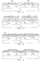
- FIGS 1-8 show sequential steps in fabrication of an integrated circuit device using the methods of the present invention.
- Figure 9 shows an alternative embodiment in which no thick field oxide is used.
- Figure 1 schematically shows a sample CMOS device structure after an N-well 102 and a P-well 104 have been fabricated in a monocrystalline substrate 100.
- Figure 2 schematically shows the structure of Figure 1, after a LOCOS field oxide 220 (patterned using an oxide/nitride active stack 221) has been grown to define active areas 210A and 210B (for PMOS and NMOS devices respectively).
- LOCOS field oxide 220 patterned using an oxide/nitride active stack 221
- Figure 3 schematically shows the structure of Figure 2, after a thin oxide 222 has been grown over the active areas 210, and has been patterned to expose channel areas 310A and 310B within the active areas 210A and 210B. (This is a nonstandard step, and the importance of these channel areas will become apparent in Figure 4.)
- Figure 4 schematically shows the structure of Figure 3, after intrinsic silicon is deposited (e.g. at 900°C, to a thickness of 1000 ⁇ ).
- the thickness of this layer can be in the range of 400-4000 ⁇ , and the deposition temperature can be in the range of 800-1000°C).
- This step is of course preceded by a cleaning step.
- This step will epitaxially deposit a thin layer 410A or 410B of monocrystalline silicon over the channel region 310A or 310B respectively, and will deposit polycrystalline silicon 412 ("poly1") everywhere else.
- Figure 5 schematically shows the structure of Figure 4, after a thin gate oxide 420 has been grown conventionally and a second polysilicon layer 430 has been conventionally deposited.
- the gate oxide 420 may be grown to e.g. 100 ⁇ over the monocrystalline channel regions 410, and will typically be slightly thicker and rougher over the polycrystalline portion 412.
- a second polysilicon layer 430 (“poly2") is then deposited, e.g. to 3500 ⁇ thick.
- Figure 6 schematically shows the structure of Figure 5, after the poly2 layer has been patterned to produce a structure which includes, inter alia, PMOS gate portions 430A and NMOS gate portions 430B.
- a salicide step can optionally be performed at this point (or optionally after source/drain implantation), to reduce the sheet resistance of poly1 regions 412 (by cladding them with silicide).
- Figure 7 schematically shows the structure of Figure 6, during two further process steps: P-type dopants are applied in a shallow heavy implant (e.g. 10 16 cm -2 of BF 2 - at 30 keV) to the area over the N-wells 102, and N-type dopants are applied in a shallow heavy implant (e.g. 5x10 15 cm -2 of As + at 20 keV) to the area over the P-wells 104. Note that these implants dope some portions of the poly1 regions 412 N+, and other regions P+.
- the poly2 layer can be used to provide a short connection from N+ poly1 to P+ poly (particularly if a saliciding step has been performed as discussed above).
- the poly2 layer will also be doped by this implant.
- the second poly layer can be doped N+ over NMOS channel regions 410B, and P+ over PMOS channel regions 410A. This eliminates the work function difference which primarily causes VLSI PMOS devices to have buried channels.
- sidewall spacers can be conventionally formed on the poly2 layer, to adjust the source/drain underlap.
- Figure 8 schematically shows the structure of Figure 7 after a final step of brief oxidation (to seal the poly and poly2 layers) and deposition of an interlevel dielectric 810 (e.g. BPSG over TEOS-deposited oxide).
- an interlevel dielectric 810 e.g. BPSG over TEOS-deposited oxide
- Processing then continues conventionally, with formation of contact holes, formation of a patterned metal layer, formation of protective overcoat, and patterning to expose bond pad locations.
- a third layer of polysilicon can be added to the process.
- two or more layers of metallization can be used, using techniques well known to those of ordinary skill in the art.
- Figure 9 shows an alternative embodiment in which no thick field oxide is used.
- a self-aligned channel-stop implant can be used to avoid the need for growth of a thick field oxide.
- a method for fabricating integrated circuit devices comprising the steps of: providing a substrate which includes at least one substantially monolithic body of semiconductor material; covering part of the surface of the monolithic body with a patterned dielectric layer, the patterned dielectric layer leaving the monolithic body exposed in transistor channel locations; forming additional semiconductor material, as monocrystalline semiconductor material on the monolithic body in the transistor channel locations, and as polycrystalline semiconductor material elsewhere; the semiconductor material being formed to a thickness which is greater than the thickness of the patterned dielectric layer; patterning the additional material to form a patterned thin film layer, and forming a gate dielectric on the additional material; forming an additional patterned conductive thin film layer on the gate dielectric; implanting dopants of a desired conductivity type into the additional material where exposed by the additional patterned conductive thin film layer; whereby monocrystalline portions of the additional material beneath the additional patterned conductive thin film layer form transistor channel regions, and polycrystalline portions of the additional material provide source and drain regions adjacent thereto.
- a method for fabricating integrated circuit devices comprising the steps of: providing a substrate which includes at least one substantially monolithic body of semiconductor material; covering part of the surface of the monolithic body with a patterned dielectric layer, the patterned dielectric layer leaving the monolithic body exposed in transistor channel locations; depositing additional semiconductor material overall, as epitaxially matched monocrystalline semiconductor material on the monolithic body in the transistor channel locations, and as polycrystalline semiconductor material elsewhere; the semiconductor material being formed to a thickness which is greater than the thickness of the patterned dielectric layer; patterning the additional material to form a patterned thin film layer, and forming a gate dielectric on the additional material; forming an additional patterned conductive thin film layer, comprising polycrystalline semiconductor material, on the gate dielectric; and implanting dopants of a desired conductivity type into the additional material where exposed by the additional patterned conductive thin film layer; whereby monocrystalline portions of the additional material beneath the additional patterned conductive thin film layer form transistor channel regions, and poly
- a method for fabricating CMOS integrated circuit devices comprising the steps of: providing a substrate which includes at least one substantially monolithic body of semiconductor material, having at least one first-conductivity-type surface region and at least one second-conductivity-type surface region; covering part of the surface of the monolithic body with a patterned dielectric layer, the patterned dielectric layer leaving the monolithic body exposed in transistor channel locations; forming additional semiconductor material, as monocrystalline semiconductor material on the monolithic body in the transistor channel locations, and as polycrystalline semiconductor material elsewhere; the semiconductor material being formed to a thickness which is greater than the thickness of the patterned dielectric layer; patterning the additional material to form a patterned thin film layer, and forming a gate dielectric on the additional material; forming an additional patterned conductive thin film layer on the gate dielectric; implanting dopants of the first conductivity type over locations of the second-conductivity-type regions of the body, and implanting dopants of the second conductivity type over locations
- an integrated circuit field-effect transistor structure comprising: a monocrystalline semiconductor channel region; a conductive gate capacitively coupled to the channel region; a monocrystalline semiconductor body region which underlies and is epitaxially continuous with the channel region; first and second polycrystalline semiconductor source/drain regions which laterally adjoin opposing sides of the channel region, and each extend continuously therefrom; and a patterned dielectric layer, which underlies the source/drain regions but not the channel region; the patterned dielectric layer being thinner than the semiconductor source/drain regions.
- the illustrated sample embodiment is a twin-tub structure, but of course this does not by any means limit the invention.
- the masking can optionally be adjusted to leave part of poly1 undoped.
- Such intrinsic material has a very high sheet resistance, and can be used for a variety of purposes (even in a CMOS structure), e.g. defining power-on states, providing low-power voltage divider chains, power-supply-dropping in very-low-power circuits, and rad-hard gates (using a resistor interposed between the two nodes of a CMOS latch).
Landscapes
- Metal-Oxide And Bipolar Metal-Oxide Semiconductor Integrated Circuits (AREA)
- Thin Film Transistor (AREA)
- Insulated Gate Type Field-Effect Transistor (AREA)
- Recrystallisation Techniques (AREA)
Applications Claiming Priority (2)
| Application Number | Priority Date | Filing Date | Title |
|---|---|---|---|
| US397654 | 1995-02-28 | ||
| US08/397,654 US5668025A (en) | 1995-02-28 | 1995-02-28 | Method of making a FET with dielectrically isolated sources and drains |
Publications (2)
| Publication Number | Publication Date |
|---|---|
| EP0730307A2 true EP0730307A2 (fr) | 1996-09-04 |
| EP0730307A3 EP0730307A3 (fr) | 1999-05-06 |
Family
ID=23572094
Family Applications (1)
| Application Number | Title | Priority Date | Filing Date |
|---|---|---|---|
| EP96301271A Withdrawn EP0730307A3 (fr) | 1995-02-28 | 1996-02-26 | Technologie d'effet de champ avec des sources et drains diélectriquement isolés |
Country Status (3)
| Country | Link |
|---|---|
| US (2) | US5668025A (fr) |
| EP (1) | EP0730307A3 (fr) |
| JP (1) | JPH08255841A (fr) |
Cited By (1)
| Publication number | Priority date | Publication date | Assignee | Title |
|---|---|---|---|---|
| WO2000019510A3 (fr) * | 1998-09-29 | 2000-07-20 | Conexant Systems Inc | Transistor mos a effet de champ a canal sureleve |
Families Citing this family (12)
| Publication number | Priority date | Publication date | Assignee | Title |
|---|---|---|---|---|
| US5773328A (en) | 1995-02-28 | 1998-06-30 | Sgs-Thomson Microelectronics, Inc. | Method of making a fully-dielectric-isolated fet |
| US6420764B1 (en) * | 1995-02-28 | 2002-07-16 | Stmicroelectronics, Inc. | Field effect transitor having dielectrically isolated sources and drains and methods for making same |
| US6198114B1 (en) | 1997-10-28 | 2001-03-06 | Stmicroelectronics, Inc. | Field effect transistor having dielectrically isolated sources and drains and method for making same |
| US6133077A (en) * | 1998-01-13 | 2000-10-17 | Lsi Logic Corporation | Formation of high-voltage and low-voltage devices on a semiconductor substrate |
| DE19845793A1 (de) * | 1998-09-21 | 2000-03-23 | Inst Halbleiterphysik Gmbh | Bipolartransistor und Verfahren zu seiner Herstellung |
| US6274445B1 (en) | 1999-02-03 | 2001-08-14 | Philips Semi-Conductor, Inc. | Method of manufacturing shallow source/drain junctions in a salicide process |
| US6613626B1 (en) * | 2000-06-27 | 2003-09-02 | Sharp Laboratories Of America, Inc. | Method of forming CMOS transistor having a deep sub-micron mid-gap metal gate |
| US7067363B2 (en) * | 2002-12-30 | 2006-06-27 | Stmicroelectronics S.R.L. | Vertical-conduction and planar-structure MOS device with a double thickness of gate oxide and method for realizing power vertical MOS transistors with improved static and dynamic performances and high scaling down density |
| JP3974542B2 (ja) * | 2003-03-17 | 2007-09-12 | 株式会社東芝 | 半導体基板の製造方法および半導体装置の製造方法 |
| JP2007329200A (ja) * | 2006-06-06 | 2007-12-20 | Toshiba Corp | 半導体装置の製造方法 |
| US8487354B2 (en) * | 2009-08-21 | 2013-07-16 | Taiwan Semiconductor Manufacturing Company, Ltd. | Method for improving selectivity of epi process |
| US10910435B2 (en) * | 2019-03-27 | 2021-02-02 | International Business Machines Corporation | Stackable symmetrical operation memory bit cell structure with bidirectional selectors |
Family Cites Families (21)
| Publication number | Priority date | Publication date | Assignee | Title |
|---|---|---|---|---|
| US4041518A (en) * | 1973-02-24 | 1977-08-09 | Hitachi, Ltd. | MIS semiconductor device and method of manufacturing the same |
| JPS52113684A (en) * | 1976-03-19 | 1977-09-22 | Matsushita Electric Ind Co Ltd | Semiconductor device |
| US4353085A (en) * | 1978-02-27 | 1982-10-05 | Fujitsu Limited | Integrated semiconductor device having insulated gate field effect transistors with a buried insulating film |
| NL8006339A (nl) * | 1979-11-21 | 1981-06-16 | Hitachi Ltd | Halfgeleiderinrichting en werkwijze voor de vervaar- diging daarvan. |
| JPS56115557A (en) * | 1980-02-18 | 1981-09-10 | Matsushita Electric Ind Co Ltd | Manufacture of semiconductor device |
| US4487639A (en) * | 1980-09-26 | 1984-12-11 | Texas Instruments Incorporated | Localized epitaxy for VLSI devices |
| EP0077737A3 (fr) * | 1981-10-19 | 1984-11-07 | FAIRCHILD CAMERA & INSTRUMENT CORPORATION | Dispositif à effet de champ à basse capacité |
| CA1197628A (fr) * | 1984-01-05 | 1985-12-03 | Thomas W. Macelwee | Fabrication de dispositifs mos empiles |
| JPS62162362A (ja) * | 1986-01-10 | 1987-07-18 | Mitsubishi Electric Corp | Mos型集積回路及びその製造方法 |
| NL190388C (nl) * | 1986-02-07 | 1994-02-01 | Nippon Telegraph & Telephone | Werkwijze voor het vervaardigen van een halfgeleiderinrichting en halfgeleiderinrichting. |
| US4874716A (en) * | 1986-04-01 | 1989-10-17 | Texas Instrument Incorporated | Process for fabricating integrated circuit structure with extremely smooth polysilicone dielectric interface |
| US4862232A (en) * | 1986-09-22 | 1989-08-29 | General Motors Corporation | Transistor structure for high temperature logic circuits with insulation around source and drain regions |
| KR900007686B1 (ko) * | 1986-10-08 | 1990-10-18 | 후지쓰 가부시끼가이샤 | 선택적으로 산화된 실리콘 기판상에 에피택셜 실리콘층과 다결정 실리콘층을 동시에 성장시키는 기상 증착방법 |
| JPS63192266A (ja) * | 1987-02-04 | 1988-08-09 | Oki Electric Ind Co Ltd | Cmos集積回路及びその製造方法 |
| JPS63304657A (ja) * | 1987-06-04 | 1988-12-12 | Fujitsu Ltd | 半導体装置の製造方法 |
| US4914053A (en) * | 1987-09-08 | 1990-04-03 | Texas Instruments Incorporated | Heteroepitaxial selective-area growth through insulator windows |
| US5132755A (en) * | 1989-07-11 | 1992-07-21 | Oki Electric Industry Co. Ltd. | Field effect transistor |
| CA2031254A1 (fr) * | 1989-12-01 | 1991-06-02 | Kenji Aoki | Methode de dopage des barrieres dans les dispositifs a semiconducteur |
| JPH0488658A (ja) * | 1990-08-01 | 1992-03-23 | Fujitsu Ltd | 半導体装置およびその製造方法 |
| US5110757A (en) * | 1990-12-19 | 1992-05-05 | North American Philips Corp. | Formation of composite monosilicon/polysilicon layer using reduced-temperature two-step silicon deposition |
| EP0809279B1 (fr) * | 1991-09-23 | 2003-02-19 | Infineon Technologies AG | Procédé pour la fabrication d'un transistor MOS |
-
1995
- 1995-02-28 US US08/397,654 patent/US5668025A/en not_active Expired - Lifetime
-
1996
- 1996-02-26 EP EP96301271A patent/EP0730307A3/fr not_active Withdrawn
- 1996-02-28 JP JP8041208A patent/JPH08255841A/ja active Pending
-
1997
- 1997-03-12 US US08/820,406 patent/US5856696A/en not_active Expired - Lifetime
Cited By (3)
| Publication number | Priority date | Publication date | Assignee | Title |
|---|---|---|---|---|
| WO2000019510A3 (fr) * | 1998-09-29 | 2000-07-20 | Conexant Systems Inc | Transistor mos a effet de champ a canal sureleve |
| US6143593A (en) * | 1998-09-29 | 2000-11-07 | Conexant Systems, Inc. | Elevated channel MOSFET |
| US6630710B1 (en) | 1998-09-29 | 2003-10-07 | Newport Fab, Llc | Elevated channel MOSFET |
Also Published As
| Publication number | Publication date |
|---|---|
| US5856696A (en) | 1999-01-05 |
| US5668025A (en) | 1997-09-16 |
| EP0730307A3 (fr) | 1999-05-06 |
| JPH08255841A (ja) | 1996-10-01 |
Similar Documents
| Publication | Publication Date | Title |
|---|---|---|
| US5981318A (en) | Fully-dielectric-isolated FET technology | |
| US5171699A (en) | Vertical DMOS transistor structure built in an N-well CMOS-based BiCMOS process and method of fabrication | |
| US7211863B2 (en) | Modular bipolar-CMOS-DMOS analog integrated circuit and power transistor technology | |
| KR100223098B1 (ko) | Bicmos 디바이스 및 그 제조방법 | |
| US7268394B2 (en) | JFET structure for integrated circuit and fabrication method | |
| US5674762A (en) | Method of fabricating an EPROM with high voltage transistors | |
| US6949424B2 (en) | Single poly-emitter PNP using DWELL diffusion in a BiCMOS technology | |
| US5668025A (en) | Method of making a FET with dielectrically isolated sources and drains | |
| WO1995001653A1 (fr) | Transistors et leur procede de fabrication | |
| US5444003A (en) | Method and structure for creating a self-aligned bicmos-compatible bipolar transistor with a laterally graded emitter structure | |
| US5893729A (en) | Method of making SOI circuit for higher temperature and higher voltage applications | |
| EP0849791A1 (fr) | Améliorations dans ou concernant des dispositifs semi-conducteurs |
Legal Events
| Date | Code | Title | Description |
|---|---|---|---|
| PUAI | Public reference made under article 153(3) epc to a published international application that has entered the european phase |
Free format text: ORIGINAL CODE: 0009012 |
|
| AK | Designated contracting states |
Kind code of ref document: A2 Designated state(s): DE FR GB IT |
|
| RAP3 | Party data changed (applicant data changed or rights of an application transferred) |
Owner name: STMICROELECTRONICS, INC. |
|
| PUAL | Search report despatched |
Free format text: ORIGINAL CODE: 0009013 |
|
| AK | Designated contracting states |
Kind code of ref document: A3 Designated state(s): DE FR GB IT |
|
| RHK1 | Main classification (correction) |
Ipc: H01L 21/336 |
|
| 17P | Request for examination filed |
Effective date: 19991020 |
|
| 17Q | First examination report despatched |
Effective date: 20050111 |
|
| STAA | Information on the status of an ep patent application or granted ep patent |
Free format text: STATUS: THE APPLICATION IS DEEMED TO BE WITHDRAWN |
|
| 18D | Application deemed to be withdrawn |
Effective date: 20070901 |