EP0730781B1 - Leiterrahmen mit mehreren leitenden schichten - Google Patents
Leiterrahmen mit mehreren leitenden schichten Download PDFInfo
- Publication number
- EP0730781B1 EP0730781B1 EP95930948A EP95930948A EP0730781B1 EP 0730781 B1 EP0730781 B1 EP 0730781B1 EP 95930948 A EP95930948 A EP 95930948A EP 95930948 A EP95930948 A EP 95930948A EP 0730781 B1 EP0730781 B1 EP 0730781B1
- Authority
- EP
- European Patent Office
- Prior art keywords
- leads
- conductive layer
- lead
- electrically conductive
- short
- Prior art date
- Legal status (The legal status is an assumption and is not a legal conclusion. Google has not performed a legal analysis and makes no representation as to the accuracy of the status listed.)
- Expired - Lifetime
Links
Images


Classifications
-
- H—ELECTRICITY
- H10—SEMICONDUCTOR DEVICES; ELECTRIC SOLID-STATE DEVICES NOT OTHERWISE PROVIDED FOR
- H10W—GENERIC PACKAGES, INTERCONNECTIONS, CONNECTORS OR OTHER CONSTRUCTIONAL DETAILS OF DEVICES COVERED BY CLASS H10
- H10W70/00—Package substrates; Interposers; Redistribution layers [RDL]
- H10W70/40—Leadframes
- H10W70/464—Additional interconnections in combination with leadframes
- H10W70/468—Circuit boards
-
- H—ELECTRICITY
- H10—SEMICONDUCTOR DEVICES; ELECTRIC SOLID-STATE DEVICES NOT OTHERWISE PROVIDED FOR
- H10W—GENERIC PACKAGES, INTERCONNECTIONS, CONNECTORS OR OTHER CONSTRUCTIONAL DETAILS OF DEVICES COVERED BY CLASS H10
- H10W72/00—Interconnections or connectors in packages
- H10W72/071—Connecting or disconnecting
- H10W72/075—Connecting or disconnecting of bond wires
- H10W72/07541—Controlling the environment, e.g. atmosphere composition or temperature
- H10W72/07554—Controlling the environment, e.g. atmosphere composition or temperature changes in dispositions
-
- H—ELECTRICITY
- H10—SEMICONDUCTOR DEVICES; ELECTRIC SOLID-STATE DEVICES NOT OTHERWISE PROVIDED FOR
- H10W—GENERIC PACKAGES, INTERCONNECTIONS, CONNECTORS OR OTHER CONSTRUCTIONAL DETAILS OF DEVICES COVERED BY CLASS H10
- H10W72/00—Interconnections or connectors in packages
- H10W72/50—Bond wires
- H10W72/541—Dispositions of bond wires
- H10W72/5449—Dispositions of bond wires not being orthogonal to a side surface of the chip, e.g. fan-out arrangements
-
- H—ELECTRICITY
- H10—SEMICONDUCTOR DEVICES; ELECTRIC SOLID-STATE DEVICES NOT OTHERWISE PROVIDED FOR
- H10W—GENERIC PACKAGES, INTERCONNECTIONS, CONNECTORS OR OTHER CONSTRUCTIONAL DETAILS OF DEVICES COVERED BY CLASS H10
- H10W72/00—Interconnections or connectors in packages
- H10W72/50—Bond wires
- H10W72/541—Dispositions of bond wires
- H10W72/547—Dispositions of multiple bond wires
-
- H—ELECTRICITY
- H10—SEMICONDUCTOR DEVICES; ELECTRIC SOLID-STATE DEVICES NOT OTHERWISE PROVIDED FOR
- H10W—GENERIC PACKAGES, INTERCONNECTIONS, CONNECTORS OR OTHER CONSTRUCTIONAL DETAILS OF DEVICES COVERED BY CLASS H10
- H10W72/00—Interconnections or connectors in packages
- H10W72/90—Bond pads, in general
- H10W72/931—Shapes of bond pads
- H10W72/932—Plan-view shape, i.e. in top view
-
- H—ELECTRICITY
- H10—SEMICONDUCTOR DEVICES; ELECTRIC SOLID-STATE DEVICES NOT OTHERWISE PROVIDED FOR
- H10W—GENERIC PACKAGES, INTERCONNECTIONS, CONNECTORS OR OTHER CONSTRUCTIONAL DETAILS OF DEVICES COVERED BY CLASS H10
- H10W74/00—Encapsulations, e.g. protective coatings
-
- H—ELECTRICITY
- H10—SEMICONDUCTOR DEVICES; ELECTRIC SOLID-STATE DEVICES NOT OTHERWISE PROVIDED FOR
- H10W—GENERIC PACKAGES, INTERCONNECTIONS, CONNECTORS OR OTHER CONSTRUCTIONAL DETAILS OF DEVICES COVERED BY CLASS H10
- H10W90/00—Package configurations
- H10W90/701—Package configurations characterised by the relative positions of pads or connectors relative to package parts
- H10W90/751—Package configurations characterised by the relative positions of pads or connectors relative to package parts of bond wires
- H10W90/756—Package configurations characterised by the relative positions of pads or connectors relative to package parts of bond wires between a chip and a stacked lead frame, conducting package substrate or heat sink
Definitions
- This invention relates generally to lead frames for use in integrated circuit packaging and more particularly, a lead frame having one or more layered conductive planes thereon is described.
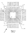
- a conventional lead frame 10 generally includes a die pad 17, die pad support arms 15 and leads 11 having lead tips 12 which circumscribe the die.
- the die pad 17, support arms 15 and long leads 11 and lead tips 12 are typically formed from a single metal strip.
- the lead forming step may be either an etching process or a stamping process. In these processes the areas between the leads 11 are removed through either stamping or etching. The area between the leads 11 and the lead tips 12 are usually referred to as slots 14.
- a mask of the pattern of leads, die pad and support arms is laid over a metal strip. The exposed areas are then etched away creating the slots 14 between the leads.
- the stamping process usually consists of stamping out the slots 14 between the leads, die pad 17 and support arms 15. Multiple stamp tool punches, shaped in the form of the respective slots 14, punch out the slots 14.
- the support arms 15 extend out from the die pad to support the die pad during handling.
- An integrated circuit is placed on the die pad 17, in the center of the lead frame 10.
- the lead frame 10 may be annealed to strengthen and relieve stress on the leads and support arms. This may be followed by plating the lead tips 12 with an electrically conductive material. Plating also allows for better bonding to the bonding wires when the leads are connected to the integrated circuit.
- the leads may then be taped with an adhesive strip to keep the leads from moving during handling.
- the adhesive strip may be a single picture frame style strip that is placed across the leads.
- An alternative is the application of separate strips placed across a set of leads. The former process allows for better tolerances when the tape either shrinks or expands causing the leads to move. Then, the lead frame 10 may be trimmed to free the lead tips 12 from the die pad 17.
- the lead frame After trimming, the lead frame is ready to be packaged. An integrated circuit is placed on the die pad 17 and bonded to the lead tips 12 with bonding wires. The inner portion of the lead frame 20 is then encapsulated with an encapsulating material. The excess metal that supported the entire lead frame 22 is then trimmed away to free the long leads 11 from each other. The end product is a packaged semiconductor device.
- a current problem with conventional lead frames is the frequency response of the leads.
- the length of the leads introduce inductance in the power and ground leads. The longer the ground and power leads the greater the inductance.
- the inductance in turn increases the amount of power consumption in a semiconductor package.
- the length also make the power and ground leads susceptible to noise from neighboring leads.
- the increased inductance makes the lead frame and the connected integrated circuit susceptible to power surges and drops.
- the inductance hampers efforts to reduce internal and external noise.
- Decoupling capacitors applied across the ground and power pins are often used to alleviate these problems. The decoupling capacitors help to filter out noise from the power supply and neighboring devices as well as protect against sudden power surges and drops.
- Semiconductor packages having a large number of pins may require two to three decoupling capacitors. The capacitors are a significant cost in products utilizing large integrated circuits.
- the frequency response of the power and ground leads should be a low pass filter.
- the inductance in the power and ground leads By decreasing the inductance in the power and ground leads and increasing the capacitance between the power and ground leads a better frequency response can be obtained.
- the improved frequency response will allow a semiconductor package to operate at high speeds. Also, the impedance of the leads are reduced which decreases power consumption.
- US Patent No. 4,891,687 to Mallik et al. discloses the use of a multilayer molded plastic integrated circuit package to obtain a compact package which had the side benefit of reducing inductance and increasing capacitance in the power and ground leads.
- Mallik teaches the use of a pair of intricate conducting layers with specialized tabs that are bonded to the leads of an otherwise ordinary lead frame that does not include a die pad.
- the specialized tabs taught in Mallik also requires that the conductive layers be precisely attached to the lead frame so that tabs align with particular leads on the lead frame. The tabs must then be bonded using relatively expensive non-standard bonding techniques.
- Mallik also requires that the integrated circuit be placed directly on the lower conductive layer.
- EP-513591 describes a lead frame in which there are alternate long and short leads connection to the long leads can be made by relatively short wires. Connection to the short leads is made by a single wire, but to avoid wire sweep the wire is additionally stitch bonded on to an insulated pier supported by the long leads.
- a lead frame comprising a plurality of long leads and a plurality of short leads, the long leads having lead tips located relatively closer to a die area than lead endsof the short leads; a first electrically conductive layer positioned, with respect to the die area, outwardly of the long lead tips and inwardly of the short lead ends and insulated from the long leads by and insulating layer, the long lead tips and the short lead ends each being exposed and accessible for wire bonding; characterised in that the conductive layer extends continuously over a plurality of the long leads and coupling of individual short leads to die pads on the die area is made via a first wire bond extending from the short lead end to a first location on the electrically conductive layer and a second wire bond extending from a second location on the electrically conductive layer to the die pad, the first and second locations being spaced apart so as to enable shorter total wire length than continuous connection, and by a second electrically conductive layer positioned over the first electrically conductive layer and insulated therefrom by a
- the invention also provides a packaged semiconductor including an integrated circuit in the die area.
- the invention further provides a method of forming a lead frame comprising the steps of: forming a plurality of long leads and a plurality of short leads from a metal strip, the long leads having lead tips located relatively closer to a die area than lead ends of the short leads; attaching first electrically conductive layer positioned, with respect to the die area, outwardly of the long lead tips and inwardly of the short lead ends and insulated from the long leads by an insulating layer, the long lead tips and the short lead ends each being exposed and accessible for wire bonding; characterised in that the conductive layer extends continuously over a plurality of the long leads and by attaching a second electrically conductive layer over the first electrically conductive layer and insulated therefrom by a second insulating layer, the second electrically conductive layer and electrically insulating layer being positioned such that exposed inner and outer ledges of the first conductive layer are located, respectively, at the edges of the first conductive layer adjacent to the long lead tips and short leads ends, the ledges being accessible for wire bonding
- the invention also includes a method for manufacturing a semiconductor package comprising the steps of: forming a lead frame using the process recited; attaching an integrated circuit die in the die area; electrically coupling the respective lead tips of the lead frame to a plurality of corresponding bonding pads on the integrated circuit; electrically coupling individual leads to the outer ledge of the first conductive layer; electrically coupling the inner ledge of the first conductive layer to individual bonding pads on the integrated circuit; electrically coupling other individual short leads to a first location on the second conductive layer; electrically coupling other individual bonding pads on the integrated circuit to a second location on the second conductive layer; and encapsulating the lead frame and the integrated circuit with an encapsulating material such that only the ends of the plurality of leads opposite the lead tips and the ends of the short leads protrude out of the encapsulating material.
- a pair of electrically conductive layer may be used, which may, for example, correspond to power and ground layers.
- the conductive layers are stacked with an electrically insulating layer therebetween.
- the second conductive layer has a smaller width than the first conductive layer and is placed over the first conductive layer. This leaves an inner ledge and an outer ledge of the first layer exposed.
- the inner ledge is electrically connected to associated bonding pads of an integrated circuit die.
- the outer ledge is electrically connected to the lead pads of the corresponding short leads.
- the second layer is also electrically connected to associated bonding pads and the lead pads.
- the electrical connections may be made with conventional bonding wires.
- the bonding pads and lead pads connected to a layer correspond to the layer they are connected to. For example, if the first layer is a ground plane layer then the bonding pads and the short leads connected to the ground plane layer are ground pads and ground leads, respectively.
- the conductive layers act as planar conductors.
- the conductive layers may correspond to ground and power planes.
- the power and ground planes separated by an insulator increases the capacitance between the power and ground planes.
- the short leads reduces inductance and the conductive planes increases capacitance in the power and ground leads.
- Decreased inductance and increased capacitance reduces the impedance in the power and ground leads. This improves the speed and power consumption of a semiconductor device using a lead frame having conductive layers with short leads.
- a multilayer lead frame 10' there are a number of long leads 11' and a plurality of short leads 111.
- the long leads 11' have lead tips 12' and the short leads 111 end in lead pads 112.
- the lead pads are merely the tips of the short leads. They do not have any special geometry, although any suitable tip geometry may be used.
- the tips of the short leads are referred to as lead pads herein only to make it easier to differentiate the tips of the long leads (referred to as lead tips) and the tips of the short lead (referred to as lead pad) in the context of this application.
- a die pad 17' and die pad support arms 15' are shown in this particular embodiment.
- the die pad 17' and the die pad support arms 15' may be omitted and an integrated circuit die may be placed in a die area at the center of the lead frame using other commonly known techniques.
- a first electrically conductive layer 118 that is placed over the lead tips 12' and die pad support arms 15' encircles the die area.
- the first electrically conductive layer 118 is placed over the long leads 11' and support arms 15' such that the it does not cover the lead tips 12'.
- the first electrically conductive layer 118 is positioned radially inside (i.e. closer to the die pad than) the lead pads 112 of the short leads 111. thereby leaving the entire short leads (including lead pads) 112 exposed.
- the short leads reduce the inductance and the conductive layers increase the capacitance between the leads connected to the conductive layer(s).
- a second conductive layer 119 is stacked on top of the first conductive layer 118 and has a smaller width than the first conductive layer. This stacking is arranged to leave an inner ledge 118a and an outer ledge 118b of the first conductive layer 118 exposed.
- the inner ledge 118a is sized suitably to permit it to be electrically connected to associated bond pads on the integrated circuit placed on the die pad 17'.
- the outer ledge 118b is sized such that it may be electrically connected to the lead pads 112 of associated short leads 111. In the embodiments shown, the electrical connections are made by wire bonding and thus, the ledges are sized suitably to permit wire bonding conventional bonding wires thereto.
- the second conductive layer 119 is also sized suitably to permit it to be electrically connected to associated bond pads on the integrated circuit and the lead pads 112 of associated short leads 111.
- the conductive layers 118 and 119 may take many shapes and forms in other embodiments.
- the conductive layers 118 and 119 may be hexagonal, or ovular rings or discrete strips coupled together such that the conductive layers 118 and 119 surround the die pad 17'.
- the conductive layers 118 and 119 may be formed in segments, semicircular or horseshoe shapes etc.
- the lead pads 112, lead tips 12', die pad, 17', support arms 15', and the conductive layers 118 and 119 are located within an encapsulation region 20'. After the encapsulation region 20' of the multilayer lead frame has been encapsulated during packaging. the excess parts of the multilayer lead frame 22' are trimmed away such that the leads 11' and 111 are separated from each other and the support arms 15.
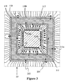
- FIG. 3 A close up view of the encapsulation region 20' of the embodiment of a multilayer lead frame shown in Figure 2 is illustrated in Figure 3 after an integrated circuit die 217 has been placed on the die pad 17.
- the die 217 has bonding pads 212 positioned in rows near the periphery of its top surface.
- the bonding pads 212 are used to electrically couple the signal, power and ground traces on the die 217 with the outside world.
- bonding wires 204 are used to electrically couple specific bonding pads 212 with associated lead tips 12' on the lead frame 10'.
- Conventional wire bonding processes can be used to electrically connect the bonding pads to the lead tips. It should be appreciated, however, that other conventional electrical connection techniques such as TAB bonding may also be utilized in conjunction with the present invention.
- all the bonding pads 212 that correspond to ground on the integrated circuit die 217 are connected to the first conductive layer 118.
- the first conductive layer 118 effectively forms a ground plane.
- all the bonding pads that correspond to power on the die 217 are connected to the second conductive layer 119.
- the second conductive layer 119 effectively forms a power plane.
- Bonding wires 204 then connect the conductive layers 118 and 119 to the associated short leads 111 through the lead pads 112.
- the designation of the conductive layers 118 and 119 as ground and power can be interchanged. It should be apparent that with the described structure, there is no need for the number of ground and power leads to exactly correspond to the number of bonding pads on the die that require connections to ground and power respectively.
- the connection to corresponding bonding pad(s) 212 can be made anywhere along the conductive plane 118 or 119.
- the location of the power and ground leads need not correspond in alignment to the location of the associated bonding pads bonding pads 212.
- one of the short power leads 111a is the third lead from the bottom of the lead frame.
- the nearest corresponding power bonding pad 212a is fifth from the bottom of the die.
- FIG. 4(a) a cross-sectional view of the multilayer lead frame shown in Figure 2 is illustrated.
- the conductive layers 118 and 119 are parallel to one another and are electrically isolated from each other and the leads 11' and 111 by the insulating layers 120, 121 respectively. More specifically, the first conductive layer 118 is secured to the long leads 11' and support arms 15' by electrically insulating adhesive layer 120. The second conductive layer 119 is secured to the first layer 118 by insulating layer 121. Any suitable adhesive insulating material such as double sided adhesive tape or non-conductive epoxy may be used to form the insulating layers.
- FIG. 5 shows an alternative embodiment utilizing a dielectric adhesive material 122.
- the conductive layers 118 and 119 may also be used to assist with the distribution of heat.
- insulating adhesive materials with good thermal conduction properties may be used in insulating layers 120 and 121.
- the described multilayer lead frame is used in packaging semiconductor devices. Initially, an integrated circuit die 217 is positioned within the die area of the lead frame and attached to it support (the die attach pad in the embodiment shown) using conventional techniques. The bond pads on die 217 are then electrically connected to the associated leads of the lead frame and to the appropriate conductive layers 118 and 119 by wire bonding or other suitable techniques. The conductive layers 118 and 119 are then electrically connected to the appropriate short leads. After encapsulation and trimming. a finished semiconductor device package is produced. A semiconductor utilizing a multilayer lead frame exhibits improved lead frequency response providing improved speed and power consumption due to the increased capacitance and reduced inductance of the multilayer lead frame with short leads. The present invention applies to all types of semiconductor device packages such as, but not limited to, dual in line pin, lead chip carrier, quad flat pack and pin grid array packages utilizing a variety of encapsulating materials ranging from plastic and ceramic to metal.
- One suitable method for manufacturing a lead frame requires in accordance with the present invention involves forming a plurality of long leads each having a lead tip and a plurality of short leads each ending in a lead pad from a metal strip. This may be done by either etching or stamping. When stamping is done, the leads 11' and 111 may then be annealed. Annealing heats the metal strip with the formed leads 11' and 111 to strengthen and relieve stresses on the leads 11' and 111. The lead tips 12' and the lead pads 212 may then be plated with a conductive coating to provide a better bonding surface.
- a first electrically conductive layer 118 is then adhered in place across the long leads 11' without covering the lead tips 12' or the lead pads 212 using an insulating adhesive tape that forms insulating layer 120.
- a second electrically conductive layer 119 having a smaller width than the first conductive layer 118, is then adhered to the top surface of the first conductive layer 118 with an insulating tape that forms insulating layer 121.
- the second conductive layer 119 is positioned over the first conductive layer 118 to leave exposed an inner ledge 118a and an outer ledge 118b of the first conductive layer 118.
- the lead frame may then be trimmed (typically after encapsulation) to remove portions of the lead frame 22' that provided structural support. thus, freeing the leads 11' and 111 from each other.
- a plurality of lead frames may be formed from a single metal strip.
- an integrated circuit die 217 is placed within a die area centrally located on the multilayer lead frame.
- the ground and power bond pads on the die 217 are electrically coupled to the appropriate conductive layers 118 and 119.
- the ground bond pads 212 are wire bonded to the inner ledge 118a of the first conductive layer.
- the outer ledge 118b of the first conductive layer 118 is then wire bonded to the lead pads 112 of the short ground leads.
- the second conductive layer 119 (which in this example takes the form of the power plane) is electrically coupled to the lead pads 112 of the short power leads 111 as well as to the power bond pads 212 on the die.
- the lead tips 12' are also electrically coupled to the associated bonding pads 212 of the die 217.
- An encapsulation region 20' is then encapsulated with a conventional encapsulating material.
- the conductive and insulating layers can be implemented in several different shapes and materials.
- the conductive layers can be any type of electrically conductive material not necessarily a metallic element. Also, more than two conductive layers can be applied in the foregoing manner or just one layer may be implemented in a particular variation of the present inventions.
- the conductive layers need not be constricted to ground and power designations.
- Another embodiment may have a conductive layer conduct a clock signal, or any other type of signal.
- the invention has been primarily described in conjunction with the use of bonding wires to electrically couple the die to the various leads and conductive layers. However, hybrid approaches that utilize other bonding techniques such as tape automated bonding can be used as well.
Landscapes
- Lead Frames For Integrated Circuits (AREA)
- Wire Bonding (AREA)
Claims (12)
- Leiterrahmen mit:dadurch gekennzeichnet, daß sich die erste elektrisch leitende Schicht kontinuierlich über eine Anzahl der langen Leitungen erstreckt und die Ankopplung einzelner kurzer Leitungen an die Bausteinflecken im Formbereich über einen ersten Verdrahtungskontakt erfolgt, der sich von dem Ende der kurzen Leitung bis zu einer ersten Stelle auf der ersten elektrisch leitenden Schicht erstreckt, und einen zweiten Verdrahtungskontakt, der sich von einer zweiten Stelle auf der ersten elektrisch leitenden Schicht bis zu dem Bausteinbereich erstreckt, wobei die erste und die zweite Stelle so voneinander beabstandet sind, daß eine kürzere Gesamtdrahtlänge als bei einer durchgehenden Verbindung ermöglicht wird, und durch eine zweite elektrisch leitende Schicht (119), die zum Bilden einer Versorgungsfläche geeignet und die über der ersten elektrisch leitenden Schicht angeordnet und von ihr durch eine zweite Isolationsschicht (121) isoliert ist, wobei die zweite elektrisch leitende Schicht und die zweite Isolationsschicht so angeordnet sind, daß die freiliegenden inneren (118a) bzw. äußeren (118b) Kanten der ersten elektrisch leitenden Schicht an den Kanten der ersten elektrisch leitenden Schicht angeordnet sind, die an die Spitzen der langen Leitungen und die Enden der kurzen Leitungen angrenzen, wobei die zweite Stelle an der inneren Kante und die erste Stelle an der äußeren Kante ist,einer Anzahl von langen Leitungen (11') und einer Anzahl von kurzen Leitungen (111), wobei die langen Leitungen Leitungsspitzen haben, die sich relativ näher an einem Bausteinbereich befinden als die Leitungsenden (112) der kurzen Leitungen;einer ersten elektrisch leitenden Schicht (118), die zum Erstellen einer Messefläche geeignet und die bezüglich des Bausteinbereichs außerhalb der Spitzen der langen Leitungen und innerhalb der Enden der kurzen Leitungen angeordnet ist und gegen die langen Leitungen durch eine Isolationsschicht (120) isoliert ist, wobei die Spitzen der langen Leitungen und die Enden der kurzen Leitungen offenliegen und zum Verdrahtungskontaktieren zugänglich sind;
wobei das Verbinden von anderen einzelnen kurzen Leitungen an Bausteinflecken im Bausteinbereich über weitere gesonderte, beabstandete Drahtkontakte durchgeführt wird, die sich von einem Ende der kurzen Leitung bzw. von einem Bausteinflecken zu beabstandeten Stellen auf der zweiten elektrisch leitenden Schicht erstrecken. - Leiterrahmen nach Anspruch 1,
bei dem die elektrisch leitenden Schichten Ringe sind, im wesentlichen rechteckige, hexagonale oder ovale Ringe, getrennte Streifen, die aneinander gekoppelt sind, um den Bausteinbereich einzuschließen, oder in Abschnitte, halbkreisförmige oder Hufeisenformen geformt sind. - Leiterrahmen nach Anspruch 1,
bei dem die erste und zweite elektrisch isolierende Schicht aus haftenden Materialien gebildet sind, die zum Kontaktieren der ersten leitenden Schicht an den Leiterrahmen bzw. der ersten leitenden Schicht an die zweite leitende Schicht geeignet sind. - Leiterrahmen nach Anspruch 1,
bei dem die zweite elektrische Isolationsschicht dielektrisch ist. - Leiterrahmen nach Anspruch 4,
bei dem die erste und zweite elektrisch leitende Schicht als Masse- und Stromflächen angeschlossen sind. - Leiterrahmen nach Anspruch 1,
bei dem eine dritte Isolationsschicht und eine dritte elektrisch leitende Schicht über die zweite elektrisch leitende Schicht gepackt sind, wobei die dritten Schichten so dimensioniert und angeordnet sind, daß sie die äußeren Kanten der zweiten elektrisch leitenden Schicht frei lassen. - Gekapselter Halbleiter mit:einem Leiterrahmen nach Anspruch 1,einer integrierten Schaltung, die in dem Bausteinbereich angeordnet ist; wobei die integrierte Schaltung eine Anzahl von Anschlußflecken hat;einer Anzahl von Kontaktdrähten zum elektrischen Ankoppeln ausgewählter Anschlußflecken der integrierten Schaltung an die zugeordneten langen Leitungen im Leiterrahmen und zum elektrischen Ankoppeln der ersten und zweiten elektrisch leitenden Schicht an die zugeordneten kurzen Leitungen; undeinem Einkapselmaterial, das die integrierte Schaltung, die Kontaktdrähte und mindestens einen Bereich des Leiterrahmens einkapselt.
- Gekapselter Halbleiter nach Anspruch 7,
der zu einem quadratisch flachen Gehäuse oder einem DIL-Gehäuse oder zu einem Leitungschipträgergehäuse oder einem Anschlußstiftrasterfeldgehäuse aufgebaut ist. - Mehrschichtiger Halbleiter nach Anspruch 7,
wobei das Einkapselmaterial ein Kunststoff oder eine Keramik ist. - Verfahren zum Erstellen eines Leiterrahmens mit den Schritten des:dadurch gekennzeichnet, daß die erste elektrisch leitende Schicht sich kontinuierlich über eine Anzahl der langen Leitungen erstreckt und durch Anbringen einer zweiten elektrisch leitenden Schicht (119), die geeignet ist, eine Stromfläche zu bilden, über der ersten elektrisch leitenden Schicht und von ihr durch eine zweite Isolationsschicht (121) isoliert, wobei die zweite elektrisch leitende Schicht und die elektrische Isolationsschicht so angeordnet sind, daß die freiliegenden inneren (118a) bzw. die äußeren (118b) Kanten der ersten elektrisch leitenden Schicht an den Kanten der ersten elektrisch leitenden Schicht angeordnet sind, die an die Spitzen der langen Leitungen und die Enden der kurzen Leitungen angrenzen, wobei die Kanten für das Drahtkontaktierten zugänglich sind.Erstellens einer Anzahl langer Leitungen (11) und einer Anzahl kurzer Leitungen (111) aus einem Metallstreifen, wobei die langen Leitungen Leitungsspitzen (12') haben, die sich relativ näher einem Bausteinbereich befinden als die Leitungsenden (112) der kurzen Leitungen;Anbringen einer ersten elektrisch leitenden Schicht (118), die zum Erstellen einer Massenfläche geeignet und die bezüglich des Bausteinbereiches außerhalb der Spitzen der langen Leitungen und innerhalb der Enden der kurzen Leitungen angeordnet und gegen die langen Leitungen durch eine Isolationsschicht (120) isoliert ist, wobei die Spitzen der langen Leitungen und die Enden der kurzen Leitungen jeweils freiliegen und für ein Drahtkontaktieren zugänglich sind;
- Verfahren nach Anspruch 10,
bei dem der Schritt des Bildens des Leiterrahmens auch einen Bausteinflecken (17) bildet, der durch eine Anzahl von Bausteinflecken-Unterstützungsarmen (15') unterstützt wird. - Verfahren zum Herstellen eines Halbleitergehäuses mit den Schritten des:Erstellens eines Leiterrahmens nach den Verfahren von Anspruch 10 oder Anspruch 11;Anbringens eines integrierten Schaltungsbausteins in dem Bausteinbereich;elektrischen Ankoppelns der entsprechenden Leitungsspitzen des Leiterrahmens an einer Anzahl von entsprechenden Kontaktanschlußflecken auf der integrierten Schaltung;elektrischen Ankoppelns einzelner Leitungen an die äußere Kante der ersten elektrisch leitenden Schicht;elektrischen Ankoppelns der inneren Kante an einzelne Kontaktanschlußflecken auf der integrierten Schaltung;elektrischen Ankoppeins anderer einzelner kurzer Leitungen an eine erste Stelle auf der zweiten elektrisch leitenden Schicht;elektrischen Ankoppeins anderer einzelner Kontaktanschlußflächen auf der integrierten Schaltung an eine zweite Stelle auf der zweiten elektrisch leitenden Schicht; undEinkapselns des Leiterrahmens und der integrierten Schaltung mit einer Vergußmasse so, daß nur die Enden der Anzahl der Leitungen, die gegenüber den Leitungsspitzen liegen, und die Enden der kurzen Leitungen aus der Vergußmasse herausragen.
Applications Claiming Priority (3)
| Application Number | Priority Date | Filing Date | Title |
|---|---|---|---|
| US294323 | 1989-01-06 | ||
| US08/294,323 US5498901A (en) | 1994-08-23 | 1994-08-23 | Lead frame having layered conductive planes |
| PCT/US1995/010785 WO1996007198A2 (en) | 1994-08-23 | 1995-08-23 | A lead frame having layered conductive planes |
Publications (2)
| Publication Number | Publication Date |
|---|---|
| EP0730781A1 EP0730781A1 (de) | 1996-09-11 |
| EP0730781B1 true EP0730781B1 (de) | 2002-11-27 |
Family
ID=23132913
Family Applications (1)
| Application Number | Title | Priority Date | Filing Date |
|---|---|---|---|
| EP95930948A Expired - Lifetime EP0730781B1 (de) | 1994-08-23 | 1995-08-23 | Leiterrahmen mit mehreren leitenden schichten |
Country Status (5)
| Country | Link |
|---|---|
| US (1) | US5498901A (de) |
| EP (1) | EP0730781B1 (de) |
| KR (1) | KR100328143B1 (de) |
| DE (1) | DE69528960T2 (de) |
| WO (1) | WO1996007198A2 (de) |
Cited By (2)
| Publication number | Priority date | Publication date | Assignee | Title |
|---|---|---|---|---|
| DE102005012642A1 (de) * | 2005-03-18 | 2006-10-05 | Dirks, Christian, Prof. | Energiespeicher zur Stützung der Versorgungsspannung einer integrierten Schaltung |
| TWI381507B (zh) * | 2009-09-18 | 2013-01-01 | 一詮精密工業股份有限公司 | Manufacturing method of lead frame |
Families Citing this family (28)
| Publication number | Priority date | Publication date | Assignee | Title |
|---|---|---|---|---|
| WO1994025979A1 (en) * | 1993-04-30 | 1994-11-10 | Lsi Logic Corporation | Integrated circuit with lead frame package having internal power and ground busses |
| JP2820645B2 (ja) * | 1994-08-30 | 1998-11-05 | アナム インダストリアル カンパニー インコーポレーティド | 半導体リードフレーム |
| US5701090A (en) * | 1994-11-15 | 1997-12-23 | Mitsubishi Denki Kabushiki Kaisha | Data output circuit with reduced output noise |
| US5818102A (en) * | 1995-12-29 | 1998-10-06 | Lsi Logic Corporation | System having integrated circuit package with lead frame having internal power and ground busses |
| JP2975979B2 (ja) * | 1996-12-30 | 1999-11-10 | アナムインダストリアル株式会社 | ボールグリッドアレイ半導体パッケージ用可撓性回路基板 |
| KR100218368B1 (ko) * | 1997-04-18 | 1999-09-01 | 구본준 | 리드프레임과 그를 이용한 반도체 패키지 및 그의 제조방법 |
| US5923995A (en) * | 1997-04-18 | 1999-07-13 | National Semiconductor Corporation | Methods and apparatuses for singulation of microelectromechanical systems |
| US5955777A (en) * | 1997-07-02 | 1999-09-21 | Micron Technology, Inc. | Lead frame assemblies with voltage reference plane and IC packages including same |
| US6159764A (en) * | 1997-07-02 | 2000-12-12 | Micron Technology, Inc. | Varied-thickness heat sink for integrated circuit (IC) packages and method of fabricating IC packages |
| AU4032197A (en) * | 1997-08-29 | 1999-03-22 | Hitachi Limited | Semiconductor device and method for manufacturing the same |
| US6002165A (en) * | 1998-02-23 | 1999-12-14 | Micron Technology, Inc. | Multilayered lead frame for semiconductor packages |
| US6130459A (en) * | 1998-03-10 | 2000-10-10 | Oryx Technology Corporation | Over-voltage protection device for integrated circuits |
| JP3171172B2 (ja) * | 1998-09-25 | 2001-05-28 | 日本電気株式会社 | 混成集積回路 |
| KR20010064907A (ko) * | 1999-12-20 | 2001-07-11 | 마이클 디. 오브라이언 | 와이어본딩 방법 및 이를 이용한 반도체패키지 |
| US6229202B1 (en) | 2000-01-10 | 2001-05-08 | Micron Technology, Inc. | Semiconductor package having downset leadframe for reducing package bow |
| TW437024B (en) | 2000-01-20 | 2001-05-28 | Advanced Semiconductor Eng | Ball grid array semiconductor package and its substrate |
| US6531784B1 (en) | 2000-06-02 | 2003-03-11 | Amkor Technology, Inc. | Semiconductor package with spacer strips |
| US6429536B1 (en) * | 2000-07-12 | 2002-08-06 | Advanced Semiconductor Engineering, Inc. | Semiconductor device |
| US6833611B2 (en) * | 2000-07-12 | 2004-12-21 | Advanced Semiconductor Engineering, Inc. | Semiconductor device |
| US6538313B1 (en) | 2001-11-13 | 2003-03-25 | National Semiconductor Corporation | IC package with integral substrate capacitor |
| US6686651B1 (en) * | 2001-11-27 | 2004-02-03 | Amkor Technology, Inc. | Multi-layer leadframe structure |
| US6998719B2 (en) * | 2003-07-30 | 2006-02-14 | Telairity Semiconductor, Inc. | Power grid layout techniques on integrated circuits |
| JP3998647B2 (ja) * | 2004-02-12 | 2007-10-31 | 株式会社東芝 | 半導体チップおよび半導体チップのテスト方法 |
| JP4628996B2 (ja) * | 2006-06-01 | 2011-02-09 | 新光電気工業株式会社 | リードフレームとその製造方法及び半導体装置 |
| TW200836315A (en) * | 2007-02-16 | 2008-09-01 | Richtek Techohnology Corp | Electronic package structure and method thereof |
| US7723159B2 (en) * | 2007-05-04 | 2010-05-25 | Stats Chippac, Ltd. | Package-on-package using through-hole via die on saw streets |
| WO2016031206A1 (ja) * | 2014-08-29 | 2016-03-03 | パナソニックIpマネジメント株式会社 | 半導体装置、実装体、車両 |
| KR101871553B1 (ko) * | 2015-11-24 | 2018-06-27 | 앰코테크놀로지코리아(주) | 반도체 디바이스 |
Family Cites Families (10)
| Publication number | Priority date | Publication date | Assignee | Title |
|---|---|---|---|---|
| US4451845A (en) * | 1981-12-22 | 1984-05-29 | Avx Corporation | Lead frame device including ceramic encapsulated capacitor and IC chip |
| US4891687A (en) * | 1987-01-12 | 1990-01-02 | Intel Corporation | Multi-layer molded plastic IC package |
| JP2587805B2 (ja) * | 1987-10-19 | 1997-03-05 | 新光電気工業株式会社 | 半導体装置 |
| US5089878A (en) * | 1989-06-09 | 1992-02-18 | Lee Jaesup N | Low impedance packaging |
| US5025114A (en) * | 1989-10-30 | 1991-06-18 | Olin Corporation | Multi-layer lead frames for integrated circuit packages |
| JPH0485836A (ja) * | 1990-07-26 | 1992-03-18 | Hitachi Ltd | 半導体装置 |
| US5194695A (en) * | 1990-11-02 | 1993-03-16 | Ak Technology, Inc. | Thermoplastic semiconductor package |
| US5168368A (en) * | 1991-05-09 | 1992-12-01 | International Business Machines Corporation | Lead frame-chip package with improved configuration |
| JPH06120408A (ja) * | 1992-10-02 | 1994-04-28 | Ricoh Co Ltd | 半導体集積装置用リードフレーム |
| US5343074A (en) * | 1993-10-04 | 1994-08-30 | Motorola, Inc. | Semiconductor device having voltage distribution ring(s) and method for making the same |
-
1994
- 1994-08-23 US US08/294,323 patent/US5498901A/en not_active Expired - Lifetime
-
1995
- 1995-08-23 EP EP95930948A patent/EP0730781B1/de not_active Expired - Lifetime
- 1995-08-23 WO PCT/US1995/010785 patent/WO1996007198A2/en not_active Ceased
- 1995-08-23 DE DE69528960T patent/DE69528960T2/de not_active Expired - Fee Related
- 1995-08-23 KR KR1019960702084A patent/KR100328143B1/ko not_active Expired - Lifetime
Cited By (2)
| Publication number | Priority date | Publication date | Assignee | Title |
|---|---|---|---|---|
| DE102005012642A1 (de) * | 2005-03-18 | 2006-10-05 | Dirks, Christian, Prof. | Energiespeicher zur Stützung der Versorgungsspannung einer integrierten Schaltung |
| TWI381507B (zh) * | 2009-09-18 | 2013-01-01 | 一詮精密工業股份有限公司 | Manufacturing method of lead frame |
Also Published As
| Publication number | Publication date |
|---|---|
| DE69528960T2 (de) | 2003-07-03 |
| WO1996007198A3 (en) | 1996-10-24 |
| WO1996007198A2 (en) | 1996-03-07 |
| KR960706194A (ko) | 1996-11-08 |
| US5498901A (en) | 1996-03-12 |
| EP0730781A1 (de) | 1996-09-11 |
| KR100328143B1 (ko) | 2002-06-26 |
| DE69528960D1 (de) | 2003-01-09 |
Similar Documents
| Publication | Publication Date | Title |
|---|---|---|
| EP0730781B1 (de) | Leiterrahmen mit mehreren leitenden schichten | |
| US4984059A (en) | Semiconductor device and a method for fabricating the same | |
| US6703696B2 (en) | Semiconductor package | |
| US4974057A (en) | Semiconductor device package with circuit board and resin | |
| US4796078A (en) | Peripheral/area wire bonding technique | |
| US6175149B1 (en) | Mounting multiple semiconductor dies in a package | |
| US4994411A (en) | Process of producing semiconductor device | |
| KR100226737B1 (ko) | 반도체소자 적층형 반도체 패키지 | |
| US4912547A (en) | Tape bonded semiconductor device | |
| US7473584B1 (en) | Method for fabricating a fan-in leadframe semiconductor package | |
| US4903114A (en) | Resin-molded semiconductor | |
| EP0764345A1 (de) | Leiterrahmen aus mehreren schichten | |
| US6791166B1 (en) | Stackable lead frame package using exposed internal lead traces | |
| US5917235A (en) | Semiconductor device having LOC structure, a semiconductor device lead frame, TAB leads, and an insulating TAB tape | |
| US6265760B1 (en) | Semiconductor device, and semiconductor device with die pad and protruding chip lead frame and method of manufacturing the same | |
| US6686651B1 (en) | Multi-layer leadframe structure | |
| JP2732767B2 (ja) | 樹脂封止型半導体装置 | |
| US5118556A (en) | Film material for film carrier manufacture and a method for manufacturing film carrier | |
| JPH07307409A (ja) | 半導体装置及びその製造方法 | |
| EP0474224B1 (de) | Halbleiteranordnung mit mehreren Halbleiterchips | |
| KR100366114B1 (ko) | 반도체장치와그의제조방법 | |
| JPS5930538Y2 (ja) | 半導体装置 | |
| JP2596399B2 (ja) | 半導体装置 | |
| JPH02211643A (ja) | 半導体装置 | |
| JP3041849B2 (ja) | 半導体装置及びその製造方法 |
Legal Events
| Date | Code | Title | Description |
|---|---|---|---|
| PUAI | Public reference made under article 153(3) epc to a published international application that has entered the european phase |
Free format text: ORIGINAL CODE: 0009012 |
|
| 17P | Request for examination filed |
Effective date: 19960510 |
|
| AK | Designated contracting states |
Kind code of ref document: A1 Designated state(s): DE FR GB |
|
| PUAK | Availability of information related to the publication of the international search report |
Free format text: ORIGINAL CODE: 0009015 |
|
| 17Q | First examination report despatched |
Effective date: 19980629 |
|
| GRAG | Despatch of communication of intention to grant |
Free format text: ORIGINAL CODE: EPIDOS AGRA |
|
| GRAG | Despatch of communication of intention to grant |
Free format text: ORIGINAL CODE: EPIDOS AGRA |
|
| GRAH | Despatch of communication of intention to grant a patent |
Free format text: ORIGINAL CODE: EPIDOS IGRA |
|
| GRAH | Despatch of communication of intention to grant a patent |
Free format text: ORIGINAL CODE: EPIDOS IGRA |
|
| GRAA | (expected) grant |
Free format text: ORIGINAL CODE: 0009210 |
|
| AK | Designated contracting states |
Kind code of ref document: B1 Designated state(s): DE FR GB |
|
| PG25 | Lapsed in a contracting state [announced via postgrant information from national office to epo] |
Ref country code: FR Free format text: LAPSE BECAUSE OF FAILURE TO SUBMIT A TRANSLATION OF THE DESCRIPTION OR TO PAY THE FEE WITHIN THE PRESCRIBED TIME-LIMIT Effective date: 20021127 |
|
| REG | Reference to a national code |
Ref country code: GB Ref legal event code: FG4D |
|
| REF | Corresponds to: |
Ref document number: 69528960 Country of ref document: DE Date of ref document: 20030109 |
|
| PG25 | Lapsed in a contracting state [announced via postgrant information from national office to epo] |
Ref country code: GB Free format text: LAPSE BECAUSE OF NON-PAYMENT OF DUE FEES Effective date: 20030823 |
|
| EN | Fr: translation not filed | ||
| PLBE | No opposition filed within time limit |
Free format text: ORIGINAL CODE: 0009261 |
|
| STAA | Information on the status of an ep patent application or granted ep patent |
Free format text: STATUS: NO OPPOSITION FILED WITHIN TIME LIMIT |
|
| 26N | No opposition filed |
Effective date: 20030828 |
|
| GBPC | Gb: european patent ceased through non-payment of renewal fee | ||
| PGFP | Annual fee paid to national office [announced via postgrant information from national office to epo] |
Ref country code: DE Payment date: 20071001 Year of fee payment: 13 |
|
| PG25 | Lapsed in a contracting state [announced via postgrant information from national office to epo] |
Ref country code: DE Free format text: LAPSE BECAUSE OF NON-PAYMENT OF DUE FEES Effective date: 20090303 |