EP0730964B1 - Verfahren zum Herstellen eines Tintenstrahlkopfes - Google Patents
Verfahren zum Herstellen eines Tintenstrahlkopfes Download PDFInfo
- Publication number
- EP0730964B1 EP0730964B1 EP96103650A EP96103650A EP0730964B1 EP 0730964 B1 EP0730964 B1 EP 0730964B1 EP 96103650 A EP96103650 A EP 96103650A EP 96103650 A EP96103650 A EP 96103650A EP 0730964 B1 EP0730964 B1 EP 0730964B1
- Authority
- EP
- European Patent Office
- Prior art keywords
- liquid
- ink jet
- solid layer
- jet head
- substrate
- Prior art date
- Legal status (The legal status is an assumption and is not a legal conclusion. Google has not performed a legal analysis and makes no representation as to the accuracy of the status listed.)
- Expired - Lifetime
Links
- 238000000034 method Methods 0.000 title claims description 32
- 239000007787 solid Substances 0.000 claims description 42
- 239000000758 substrate Substances 0.000 claims description 33
- 239000000463 material Substances 0.000 claims description 27
- 239000007788 liquid Substances 0.000 claims description 20
- 229920005989 resin Polymers 0.000 claims description 13
- 239000011347 resin Substances 0.000 claims description 13
- 238000007599 discharging Methods 0.000 claims description 3
- 239000003513 alkali Substances 0.000 claims 1
- 238000001723 curing Methods 0.000 claims 1
- 238000013007 heat curing Methods 0.000 claims 1
- QVEIBLDXZNGPHR-UHFFFAOYSA-N naphthalene-1,4-dione;diazide Chemical class [N-]=[N+]=[N-].[N-]=[N+]=[N-].C1=CC=C2C(=O)C=CC(=O)C2=C1 QVEIBLDXZNGPHR-UHFFFAOYSA-N 0.000 claims 1
- 238000003847 radiation curing Methods 0.000 claims 1
- HEMHJVSKTPXQMS-UHFFFAOYSA-M Sodium hydroxide Chemical compound [OH-].[Na+] HEMHJVSKTPXQMS-UHFFFAOYSA-M 0.000 description 42
- 239000007864 aqueous solution Substances 0.000 description 13
- 238000007639 printing Methods 0.000 description 13
- 239000011248 coating agent Substances 0.000 description 11
- 238000000576 coating method Methods 0.000 description 11
- XLYOFNOQVPJJNP-UHFFFAOYSA-N water Substances O XLYOFNOQVPJJNP-UHFFFAOYSA-N 0.000 description 11
- 239000003822 epoxy resin Substances 0.000 description 7
- 229920000647 polyepoxide Polymers 0.000 description 7
- 239000000047 product Substances 0.000 description 7
- 230000003287 optical effect Effects 0.000 description 6
- 239000003795 chemical substances by application Substances 0.000 description 5
- 238000004519 manufacturing process Methods 0.000 description 5
- 229920002120 photoresistant polymer Polymers 0.000 description 5
- CSCPPACGZOOCGX-UHFFFAOYSA-N Acetone Chemical compound CC(C)=O CSCPPACGZOOCGX-UHFFFAOYSA-N 0.000 description 4
- QVGXLLKOCUKJST-UHFFFAOYSA-N atomic oxygen Chemical compound [O] QVGXLLKOCUKJST-UHFFFAOYSA-N 0.000 description 4
- 239000011521 glass Substances 0.000 description 4
- 229910052760 oxygen Inorganic materials 0.000 description 4
- 239000001301 oxygen Substances 0.000 description 4
- 238000001020 plasma etching Methods 0.000 description 4
- 238000010276 construction Methods 0.000 description 3
- 239000000243 solution Substances 0.000 description 3
- 229920001342 Bakelite® Polymers 0.000 description 2
- 239000004593 Epoxy Substances 0.000 description 2
- XUIMIQQOPSSXEZ-UHFFFAOYSA-N Silicon Chemical compound [Si] XUIMIQQOPSSXEZ-UHFFFAOYSA-N 0.000 description 2
- -1 Triphenylsulfonium hexafluoroantimonate Chemical compound 0.000 description 2
- 238000012769 bulk production Methods 0.000 description 2
- 230000007547 defect Effects 0.000 description 2
- 230000000694 effects Effects 0.000 description 2
- 238000005530 etching Methods 0.000 description 2
- LNEPOXFFQSENCJ-UHFFFAOYSA-N haloperidol Chemical compound C1CC(O)(C=2C=CC(Cl)=CC=2)CCN1CCCC(=O)C1=CC=C(F)C=C1 LNEPOXFFQSENCJ-UHFFFAOYSA-N 0.000 description 2
- 238000007641 inkjet printing Methods 0.000 description 2
- 238000000059 patterning Methods 0.000 description 2
- 238000000206 photolithography Methods 0.000 description 2
- 238000007747 plating Methods 0.000 description 2
- 238000005498 polishing Methods 0.000 description 2
- 229910052710 silicon Inorganic materials 0.000 description 2
- 239000010703 silicon Substances 0.000 description 2
- 238000004528 spin coating Methods 0.000 description 2
- 238000001721 transfer moulding Methods 0.000 description 2
- KUBDPQJOLOUJRM-UHFFFAOYSA-N 2-(chloromethyl)oxirane;4-[2-(4-hydroxyphenyl)propan-2-yl]phenol Chemical compound ClCC1CO1.C=1C=C(O)C=CC=1C(C)(C)C1=CC=C(O)C=C1 KUBDPQJOLOUJRM-UHFFFAOYSA-N 0.000 description 1
- BLRPTPMANUNPDV-UHFFFAOYSA-N Silane Chemical compound [SiH4] BLRPTPMANUNPDV-UHFFFAOYSA-N 0.000 description 1
- 235000010724 Wisteria floribunda Nutrition 0.000 description 1
- 238000013019 agitation Methods 0.000 description 1
- 230000015572 biosynthetic process Effects 0.000 description 1
- 238000005520 cutting process Methods 0.000 description 1
- 238000001312 dry etching Methods 0.000 description 1
- 239000000428 dust Substances 0.000 description 1
- 238000005323 electroforming Methods 0.000 description 1
- 239000012467 final product Substances 0.000 description 1
- 239000003094 microcapsule Substances 0.000 description 1
- 239000000203 mixture Substances 0.000 description 1
- 239000003960 organic solvent Substances 0.000 description 1
- 239000011342 resin composition Substances 0.000 description 1
- 239000004065 semiconductor Substances 0.000 description 1
- 229910000077 silane Inorganic materials 0.000 description 1
- 239000002904 solvent Substances 0.000 description 1
- 238000004544 sputter deposition Methods 0.000 description 1
- 239000000126 substance Substances 0.000 description 1
- 238000004381 surface treatment Methods 0.000 description 1
- BPSIOYPQMFLKFR-UHFFFAOYSA-N trimethoxy-[3-(oxiran-2-ylmethoxy)propyl]silane Chemical compound CO[Si](OC)(OC)CCCOCC1CO1 BPSIOYPQMFLKFR-UHFFFAOYSA-N 0.000 description 1
- 238000007740 vapor deposition Methods 0.000 description 1
- 238000005406 washing Methods 0.000 description 1
Images

Classifications
-
- B—PERFORMING OPERATIONS; TRANSPORTING
- B41—PRINTING; LINING MACHINES; TYPEWRITERS; STAMPS
- B41J—TYPEWRITERS; SELECTIVE PRINTING MECHANISMS, i.e. MECHANISMS PRINTING OTHERWISE THAN FROM A FORME; CORRECTION OF TYPOGRAPHICAL ERRORS
- B41J2/00—Typewriters or selective printing mechanisms characterised by the printing or marking process for which they are designed
- B41J2/005—Typewriters or selective printing mechanisms characterised by the printing or marking process for which they are designed characterised by bringing liquid or particles selectively into contact with a printing material
- B41J2/01—Ink jet
- B41J2/135—Nozzles
- B41J2/16—Production of nozzles
- B41J2/1601—Production of bubble jet print heads
- B41J2/1603—Production of bubble jet print heads of the front shooter type
-
- B—PERFORMING OPERATIONS; TRANSPORTING
- B41—PRINTING; LINING MACHINES; TYPEWRITERS; STAMPS
- B41J—TYPEWRITERS; SELECTIVE PRINTING MECHANISMS, i.e. MECHANISMS PRINTING OTHERWISE THAN FROM A FORME; CORRECTION OF TYPOGRAPHICAL ERRORS
- B41J2/00—Typewriters or selective printing mechanisms characterised by the printing or marking process for which they are designed
- B41J2/005—Typewriters or selective printing mechanisms characterised by the printing or marking process for which they are designed characterised by bringing liquid or particles selectively into contact with a printing material
- B41J2/01—Ink jet
- B41J2/135—Nozzles
- B41J2/16—Production of nozzles
- B41J2/1621—Manufacturing processes
- B41J2/1626—Manufacturing processes etching
-
- B—PERFORMING OPERATIONS; TRANSPORTING
- B41—PRINTING; LINING MACHINES; TYPEWRITERS; STAMPS
- B41J—TYPEWRITERS; SELECTIVE PRINTING MECHANISMS, i.e. MECHANISMS PRINTING OTHERWISE THAN FROM A FORME; CORRECTION OF TYPOGRAPHICAL ERRORS
- B41J2/00—Typewriters or selective printing mechanisms characterised by the printing or marking process for which they are designed
- B41J2/005—Typewriters or selective printing mechanisms characterised by the printing or marking process for which they are designed characterised by bringing liquid or particles selectively into contact with a printing material
- B41J2/01—Ink jet
- B41J2/135—Nozzles
- B41J2/16—Production of nozzles
- B41J2/1621—Manufacturing processes
- B41J2/1631—Manufacturing processes photolithography
-
- B—PERFORMING OPERATIONS; TRANSPORTING
- B41—PRINTING; LINING MACHINES; TYPEWRITERS; STAMPS
- B41J—TYPEWRITERS; SELECTIVE PRINTING MECHANISMS, i.e. MECHANISMS PRINTING OTHERWISE THAN FROM A FORME; CORRECTION OF TYPOGRAPHICAL ERRORS
- B41J2/00—Typewriters or selective printing mechanisms characterised by the printing or marking process for which they are designed
- B41J2/005—Typewriters or selective printing mechanisms characterised by the printing or marking process for which they are designed characterised by bringing liquid or particles selectively into contact with a printing material
- B41J2/01—Ink jet
- B41J2/135—Nozzles
- B41J2/16—Production of nozzles
- B41J2/1621—Manufacturing processes
- B41J2/1632—Manufacturing processes machining
-
- B—PERFORMING OPERATIONS; TRANSPORTING
- B41—PRINTING; LINING MACHINES; TYPEWRITERS; STAMPS
- B41J—TYPEWRITERS; SELECTIVE PRINTING MECHANISMS, i.e. MECHANISMS PRINTING OTHERWISE THAN FROM A FORME; CORRECTION OF TYPOGRAPHICAL ERRORS
- B41J2/00—Typewriters or selective printing mechanisms characterised by the printing or marking process for which they are designed
- B41J2/005—Typewriters or selective printing mechanisms characterised by the printing or marking process for which they are designed characterised by bringing liquid or particles selectively into contact with a printing material
- B41J2/01—Ink jet
- B41J2/135—Nozzles
- B41J2/16—Production of nozzles
- B41J2/1621—Manufacturing processes
- B41J2/1637—Manufacturing processes molding
- B41J2/1639—Manufacturing processes molding sacrificial molding
-
- B—PERFORMING OPERATIONS; TRANSPORTING
- B41—PRINTING; LINING MACHINES; TYPEWRITERS; STAMPS
- B41J—TYPEWRITERS; SELECTIVE PRINTING MECHANISMS, i.e. MECHANISMS PRINTING OTHERWISE THAN FROM A FORME; CORRECTION OF TYPOGRAPHICAL ERRORS
- B41J2/00—Typewriters or selective printing mechanisms characterised by the printing or marking process for which they are designed
- B41J2/005—Typewriters or selective printing mechanisms characterised by the printing or marking process for which they are designed characterised by bringing liquid or particles selectively into contact with a printing material
- B41J2/01—Ink jet
- B41J2/135—Nozzles
- B41J2/16—Production of nozzles
- B41J2/1621—Manufacturing processes
- B41J2/164—Manufacturing processes thin film formation
- B41J2/1642—Manufacturing processes thin film formation thin film formation by CVD [chemical vapor deposition]
-
- B—PERFORMING OPERATIONS; TRANSPORTING
- B41—PRINTING; LINING MACHINES; TYPEWRITERS; STAMPS
- B41J—TYPEWRITERS; SELECTIVE PRINTING MECHANISMS, i.e. MECHANISMS PRINTING OTHERWISE THAN FROM A FORME; CORRECTION OF TYPOGRAPHICAL ERRORS
- B41J2/00—Typewriters or selective printing mechanisms characterised by the printing or marking process for which they are designed
- B41J2/005—Typewriters or selective printing mechanisms characterised by the printing or marking process for which they are designed characterised by bringing liquid or particles selectively into contact with a printing material
- B41J2/01—Ink jet
- B41J2/135—Nozzles
- B41J2/16—Production of nozzles
- B41J2/1621—Manufacturing processes
- B41J2/164—Manufacturing processes thin film formation
- B41J2/1643—Manufacturing processes thin film formation thin film formation by plating
-
- B—PERFORMING OPERATIONS; TRANSPORTING
- B41—PRINTING; LINING MACHINES; TYPEWRITERS; STAMPS
- B41J—TYPEWRITERS; SELECTIVE PRINTING MECHANISMS, i.e. MECHANISMS PRINTING OTHERWISE THAN FROM A FORME; CORRECTION OF TYPOGRAPHICAL ERRORS
- B41J2/00—Typewriters or selective printing mechanisms characterised by the printing or marking process for which they are designed
- B41J2/005—Typewriters or selective printing mechanisms characterised by the printing or marking process for which they are designed characterised by bringing liquid or particles selectively into contact with a printing material
- B41J2/01—Ink jet
- B41J2/135—Nozzles
- B41J2/16—Production of nozzles
- B41J2/1621—Manufacturing processes
- B41J2/164—Manufacturing processes thin film formation
- B41J2/1645—Manufacturing processes thin film formation thin film formation by spincoating
-
- B—PERFORMING OPERATIONS; TRANSPORTING
- B41—PRINTING; LINING MACHINES; TYPEWRITERS; STAMPS
- B41J—TYPEWRITERS; SELECTIVE PRINTING MECHANISMS, i.e. MECHANISMS PRINTING OTHERWISE THAN FROM A FORME; CORRECTION OF TYPOGRAPHICAL ERRORS
- B41J2/00—Typewriters or selective printing mechanisms characterised by the printing or marking process for which they are designed
- B41J2/005—Typewriters or selective printing mechanisms characterised by the printing or marking process for which they are designed characterised by bringing liquid or particles selectively into contact with a printing material
- B41J2/01—Ink jet
- B41J2/135—Nozzles
- B41J2/16—Production of nozzles
- B41J2/1621—Manufacturing processes
- B41J2/164—Manufacturing processes thin film formation
- B41J2/1646—Manufacturing processes thin film formation thin film formation by sputtering
-
- Y—GENERAL TAGGING OF NEW TECHNOLOGICAL DEVELOPMENTS; GENERAL TAGGING OF CROSS-SECTIONAL TECHNOLOGIES SPANNING OVER SEVERAL SECTIONS OF THE IPC; TECHNICAL SUBJECTS COVERED BY FORMER USPC CROSS-REFERENCE ART COLLECTIONS [XRACs] AND DIGESTS
- Y10—TECHNICAL SUBJECTS COVERED BY FORMER USPC
- Y10T—TECHNICAL SUBJECTS COVERED BY FORMER US CLASSIFICATION
- Y10T29/00—Metal working
- Y10T29/49—Method of mechanical manufacture
- Y10T29/49002—Electrical device making
- Y10T29/49082—Resistor making
- Y10T29/49083—Heater type
-
- Y—GENERAL TAGGING OF NEW TECHNOLOGICAL DEVELOPMENTS; GENERAL TAGGING OF CROSS-SECTIONAL TECHNOLOGIES SPANNING OVER SEVERAL SECTIONS OF THE IPC; TECHNICAL SUBJECTS COVERED BY FORMER USPC CROSS-REFERENCE ART COLLECTIONS [XRACs] AND DIGESTS
- Y10—TECHNICAL SUBJECTS COVERED BY FORMER USPC
- Y10T—TECHNICAL SUBJECTS COVERED BY FORMER US CLASSIFICATION
- Y10T29/00—Metal working
- Y10T29/49—Method of mechanical manufacture
- Y10T29/49401—Fluid pattern dispersing device making, e.g., ink jet
Definitions
- Ink jet heads used in ink jet printing systems are commonly provided with fine discharge openings from which printing droplets are discharged, liquid-flow paths, and liquid-discharge energy generating portions.
- such ink jet heads are roughly grouped into two forms, one of which is what is called an edge shooter type ink jet head, where the direction of growth of bubbles and the direction of discharge thereof are different, and the other of which is what is called a side shooter type ink jet head, where the direction of growth of bubbles and the direction of discharge thereof are substantially the same.
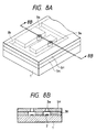
- the side shooter type ink jet head is commonly constructed as shown in Figs. 8A and 8B.
- a process for producing such a side shooter type ink jet head for example, a process is known in which a negative type photosensitive dry film is stuck to a substrate provided with the liquid-discharge energy generating element, and the photosensitive dry film is masked in a pattern corresponding to a liquid-flow path and a liquid chamber, which is then exposed to light, followed by development to form the liquid-flow path wall, and next a discharge opening plate 5H produced by electroforming of Ni or the like, provided with the discharge openings, is joined to the substrate via the flow path wall.
- a discharge opening plate 5H produced by electroforming of Ni or the like
- U.S. Patent No. 5,478,606 discloses a process in which a soluble resin is used to form a liquid-flow path pattern on a substrate provided with liquid-discharge energy generating elements, then a coating resin layer which is to serve as ink-flow path walls and a discharge opening plate is formed by spin coating, thereafter the coating resin layer is cured and at the same time discharge openings are formed, and finally the pattern is dissolved away.
- the discharge openings are formed by photolithography or oxygen plasma etching or using an excimer laser after the coating resin layer has been formed, and hence it is unnecessary to make precise alignment to join the discharge opening plate to the substrate.
- this process has been sought to be further improved in view of material selectivity and improvement in productivity.
- the present invention was made taking account of the problems discussed above, and an object thereof is to provide a process for producing an ink jet head, that can achieve inexpensive bulk production of ink jet heads.
- Another object of the present invention is to provide a process for producing an ink jet head, that can achieve a broad material selectivity for flow path wall materials and promise a superior productivity.
- the products can be obtained through simple steps, in a shorter time and through a smaller number of steps.
- the process has the effect of achieving a superior bulk productivity and also reducing the cost of products.
- Figs. 1A and 1B illustrate an example of the construction of an ink jet head produced in Example 1 of the present invention.
- Figs. 3A to 3C illustrate a process of producing the ink jet head of Example 1 of the present invention.
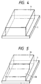
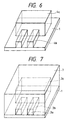
- Figs. 4 to 7 illustrate a process of producing an ink jet head in Examples 3 to 7 of the present invention.
- a liquid-discharge energy generating element 2 On a substrate 1, a liquid-discharge energy generating element 2 is provided. In a coating resin layer 3 serving as a liquid-flow path wall, a discharge opening 3a and a liquid-flow path 3b are formed.
- the substrate 1 any known substrates such as a silicon wafer may be used.
- the liquid-discharge energy generating element 2 any known elements such as an electrothermal transducer may be used.
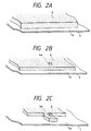
- Figs. 2A to 2C illustrate a process of forming the solid layer in the present invention.
- the solid layer 4 is optionally subjected to whole area exposure, deaeration or the like.
- the resulting substrate 1 is put on a spin coater to coat a curable material 3 which is to form a coating resin layer (Fig. 3A).
- the curable material is coated in a thickness larger than the layer thickness of the solid layer 4.
- the curable material 3 is cured, and then the cured material is evenly removed by a method such as polishing or etching until the top of the convex portion of the solid layer is laid bare to the surface (Fig. 3B).
- the solid layer 4 is dissolved away, and thus the ink jet head is completed (Fig. 3C).
- the curable material is coated in a little larger thickness and thereafter the cured material is evenly removed to have a predetermined thickness, and hence the discharge opening can have a smooth face, bringing about the advantage that the ink may hardly stand there.
- the solid layer 4 is inside the liquid-flow path 3b playing an important role in the ink jet head. This is preferable because of the advantage that the problem of ink flow path clogging due to cuttings, dust and so forth can be solved.
- the ink jet head is subsequently subjected to various steps such as washing and surface treatment and is fitted with auxiliary parts such as a filter to make up a final product.
- auxiliary parts such as a filter
- patternwise exposure was applied at a proper exposure dose using a mask aligner (PLA-501, trade name; available from Canon Inc.) via a mask pattern corresponding to nozzles and liquid chambers, followed by development by the use of an aqueous solution of 0.75% by weight of sodium hydroxide.
- This step was carried out using two kinds of masks and two kinds of exposure dose to form a resist pattern with a convex shape. Subsequently, this was rinsed with ion-exchanged water, followed by post-baking at 70°C for 30 minutes to obtain a resist pattern.
- the resist pattern was subjected to whole area exposure, and thereafter the following curable material was coated on the resist pattern by means of a spin coater.
- the spin coating was stepwise carried out under conditions of 450 rpm for 20 seconds plus 1,500 rpm for 1 second.
- the resin composition was cured at 80°C in 2 hours.
- the cured material was polished until the tops of convex portions of the solid layer appeared. After the polishing, the product was immersed in acetone to dissolve away the resist.
- a side shooter type ink jet head was produced in the same manner as in Example 1 except that the following was used as the curing agent of the curable resin.
- FUJICURE 6010 (trade name; available from Fuji Chemical Co., Ltd.) 50 parts (by weight)
- the face of discharge openings of the ink jet head thus produced was observed using an optical microscope to confirm that a highly reliable product was obtained which was free of defects such as cracks, break and scratches, free of residual resist and also free of peeling due to temperature changes.
- the printing was tested under conditions of a nozzle density of 360 DPI with 1,344 nozzles in number, and a discharge frequency of 2.84 kHz, using a water-based DEG 15% ink (containing 3% by weight of a dye). As a result, stable printing was performed.
- the products can be obtained through simple steps, in a shorter time and through a smaller number of steps, and hence, the process has the effect of achieving a superior bulk productivity and also reducing the cost of products.
- the solid layer at the part where the liquid-flow path is formed and the solid layer at the part where the discharge opening is formed are integrally formed.
- the solid layer at the part where the liquid-flow path is formed and the solid layer at the part where the liquid chamber is formed are integrally formed. The latter will be described below by giving Examples.
- a positive type photoresist AZ-4903 (trade name; available from Hoechst Japan Ltd.) was spin coated so as to be in a layer thickness of 50 ⁇ m, followed by pre-baking in an oven at 90°C for 40 minutes to form a resist layer 4 (Fig. 4).
- this resist pattern was subjected to whole area exposure at an exposure dose of 800 mJ/cm 2 , and further to deaeration for 30 minutes under vacuum condition of 0.1 mmHg.
- a photocurable material comprised of the following epoxy resins available from Union Carbide Japan K.K.: CYRACURE UVR-6110 (trade name) 40 parts CYRACURE UVR-6200 (trade name) 20 parts CYRACURE UVR-6351 (trade name) 40 parts (all by weight) and the following curing agent: Triphenylsulfonium hexafluoroantimonate 1 part (by weight) was coated, followed by whole area exposure at an exposure dose of 8.5 J/cm 2 to cause the coating to cure. Subsequently, the substrate thus treated was immersed in an aqueous solution of 3.0% by weight of sodium hydroxide to dissolve away the resist pattern (Fig. 7).
- a positive type photoresist PMER-PG7900 (trade name; available from Tokyo Ohka Kogyo Co., Ltd.) was spin coated so as to be in a layer thickness of 50 ⁇ m, followed by pre-baking in an oven at 90°C for 40 minutes to form a resist layer.
- this resist pattern was subjected to whole area exposure at an exposure dose of 1.0 J/cm 2 , and further to deaeration for 30 minutes under vacuum condition of 0.1 mmHg.
- a photocurable material comprised of the following epoxy resins available from Union Carbide Japan K.K.: CYRACURE UVR-6110 (trade name) 40 parts CYRACURE UVR-6200 (trade name) 20 parts CYRACURE UVR-6351 (trade name) 40 parts (all by weight) and the following curing agent: Triphenylsulfonium hexafluoroantimonate 1 part (by weight) was coated, followed by whole area exposure at an exposure dose of 8.5 J/cm 2 to cause the coating to cure. Subsequently, the substrate thus treated was immersed in an aqueous solution of 3.0% by weight of sodium hydroxide to dissolve away the resist pattern.
- Nozzles thus prepared were those having a very high precision and a high reliability. Also, the ink jet head thus produced enabled stable printing.
- Nozzles thus prepared were those having a very high precision and a high reliability. Also, the ink jet head thus produced enabled stable printing.
- a positive type photoresist PMER-PG7900 (trade name; available from Tokyo Ohka Kogyo Co., Ltd.) was spin coated so as to be in a layer thickness of 50 ⁇ m, followed by pre-baking in an oven at 90°C for 40 minutes to form a resist layer.
- patternwise exposure was applied at an exposure dose of 900 mJ/cm 2 using a mask aligner PLA-501 (trade name; available from Canon Inc.) via a mask pattern whose part corresponding to liquid chambers was light-screened, followed by development by the use of an aqueous solution of 1.25% by weight of sodium hydroxide. Then, the pattern formed was rinsed with ion-exchanged water, followed by post-baking in a vacuum oven at 50°C for 30 minutes to obtain a resist pattern with a liquid-flow path forming part developed by 25 ⁇ m in depth.
- PLA-501 trade name; available from Canon Inc.
Landscapes
- Engineering & Computer Science (AREA)
- Manufacturing & Machinery (AREA)
- Particle Formation And Scattering Control In Inkjet Printers (AREA)
Claims (6)
- Verfahren zur Herstellung eines Tintenstrahlkopfes, der ein Flüssigkeit ausstoßendes, Energie erzeugendes Element (2) zum Ausstoßen einer Flüssigkeit, eine Ausstoßöffnung (3a), die über dem Flüssigkeit ausstoßenden, Energie erzeugenden Element (2) vorgesehen ist und aus dem die Flüssigkeit ausgestoßen wird, einen Flüssigkeits-Durchflussweg (3b), der mit der Ausstoßöffnung (3a) verbunden ist und im Inneren mit dem Flüssigkeit ausstoßenden, Energie erzeugenden Element (2) versehen ist, und ein Substrat (1) zum Halten des Flüssigkeit ausstoßenden, Energie erzeugenden Elements (2) umfasst, wobei das Verfahren die folgenden Schritte umfasst:Herstellen des Substrats (1);Bereitstellen des Flüssigkeit ausstoßenden, Energie erzeugenden Elements (2) auf dem Substrat (1);Bereitstellen einer festen Schicht (4) mit einer konvexen Form (4a) auf der Oberfläche des Substrats (1), wo das Flüssigkeit ausstoßende, Energie erzeugende Element (2) versehen worden ist sowie auf dem Bereich, wo der Flüssigkeits-Durchflussweg (3b) und die Ausstoßöffnung (3a) vorzusehen sind, wobei die feste Schicht aus einem Harz gebildet ist, das weggelöst werden kann;Aufbringen eines härtbaren Materials (3) auf das mit der festen Schicht (4) versehene Substrat (1) in einer Dicke, die größer als die Dicke der festen Schicht ist, um die feste Schicht (4) zu bedecken;Härten des härtbaren Materials (3);gleichmäßiges Entfernen des gehärteten Materials, bis die konvexe Form (4a) der festen Schicht (4) bloß liegt; undWeglösen der festen Schicht (4), um den Flüssigkeits-Durchflussweg (3b) und die Ausstoßöffnung (3a) zu bilden.
- Verfahren zur Herstellung eines Tintenstrahlkopfes nach Anspruch 1, wobei die feste Schicht (4) mit einer konvexen Form (4a) durch das Unterwerfen eines Positivresists einer jeweils zweimaligen Belichtung und Entwicklung gebildet wird, wobei das Belichtungsmuster beim zweiten Mal innerhalb des Bereichs des Belichtungsmusters beim ersten Mal ist und gegenüber dem Belichtungsmuster beim ersten Mal unterschiedlich ist.
- Verfahren zur Herstellung eines Tintenstrahlkopfes nach Anspruch 1, wobei das härtbare Material ein Material vom Wirkenergie-Bestrahlungshärtungstypus ist.
- Verfahren zur Herstellung eines Tintenstrahlkopfes nach Anspruch 1, wobei das härtbare Material ein Material vom Wärmehärtungstypus ist.
- Verfahren zur Herstellung eines Tintenstrahlkopfes nach Anspruch 2, wobei der Positivresist unter Verwendung einer wässrigen Alkalilösung entwickelt wird.
- Verfahren zur Herstellung eines Tintenstrahlkopfes nach Anspruch 2, wobei der Positivresist ein Naphthochinondiazid-Derivat enthält.
Applications Claiming Priority (6)
| Application Number | Priority Date | Filing Date | Title |
|---|---|---|---|
| JP5107995 | 1995-03-10 | ||
| JP5107995 | 1995-03-10 | ||
| JP51079/95 | 1995-03-10 | ||
| JP171979/95 | 1995-07-07 | ||
| JP17197995 | 1995-07-07 | ||
| JP17197995 | 1995-07-07 |
Publications (3)
| Publication Number | Publication Date |
|---|---|
| EP0730964A2 EP0730964A2 (de) | 1996-09-11 |
| EP0730964A3 EP0730964A3 (de) | 1997-05-28 |
| EP0730964B1 true EP0730964B1 (de) | 2000-06-07 |
Family
ID=26391605
Family Applications (1)
| Application Number | Title | Priority Date | Filing Date |
|---|---|---|---|
| EP96103650A Expired - Lifetime EP0730964B1 (de) | 1995-03-10 | 1996-03-08 | Verfahren zum Herstellen eines Tintenstrahlkopfes |
Country Status (3)
| Country | Link |
|---|---|
| US (1) | US5983486A (de) |
| EP (1) | EP0730964B1 (de) |
| DE (1) | DE69608720T2 (de) |
Families Citing this family (11)
| Publication number | Priority date | Publication date | Assignee | Title |
|---|---|---|---|---|
| US5980026A (en) | 1995-06-14 | 1999-11-09 | Canon Kabushiki Kaisha | Process for production of ink jet head |
| JP2002144584A (ja) * | 2000-11-07 | 2002-05-21 | Sony Corp | プリンタ、プリンタヘッド及びプリンタヘッドの製造方法 |
| JP4221638B2 (ja) * | 2001-02-16 | 2009-02-12 | ソニー株式会社 | プリンタヘッドの製造方法及び静電アクチュエータの製造方法 |
| US6993840B2 (en) * | 2002-07-18 | 2006-02-07 | Canon Kabushiki Kaisha | Manufacturing method of liquid jet head |
| TW577819B (en) * | 2002-10-22 | 2004-03-01 | Nanodynamics Inc | Method for self-aligning nozzle orifice of inkjet print head |
| US6773869B1 (en) | 2003-04-24 | 2004-08-10 | Lexmark International, Inc. | Inkjet printhead nozzle plate |
| US7340831B2 (en) * | 2003-07-18 | 2008-03-11 | Canon Kabushiki Kaisha | Method for making liquid discharge head |
| US7254890B2 (en) * | 2004-12-30 | 2007-08-14 | Lexmark International, Inc. | Method of making a microfluid ejection head structure |
| US7406740B2 (en) * | 2006-09-18 | 2008-08-05 | Pallatheri Subramanian | Dusting and cleaning device |
| US20080066250A1 (en) * | 2006-09-18 | 2008-03-20 | Subramanian Pallatheri M | Dusting and Cleaning Device |
| JP5701014B2 (ja) * | 2010-11-05 | 2015-04-15 | キヤノン株式会社 | 吐出素子基板の製造方法 |
Family Cites Families (6)
| Publication number | Priority date | Publication date | Assignee | Title |
|---|---|---|---|---|
| DE69123932T2 (de) * | 1990-10-18 | 1997-05-22 | Canon Kk | Herstellungsverfahren eines Tintenstrahldruckkopfes |
| EP0488675A1 (de) * | 1990-11-28 | 1992-06-03 | Canon Kabushiki Kaisha | Herstellungsverfahren eines Farbstrahlaufzeichnungskopfes und Farbstrahlaufzeichnungskopf |
| US5443942A (en) * | 1990-11-28 | 1995-08-22 | Canon Kabushiki Kaisha | Process for removing resist |
| JP3143307B2 (ja) * | 1993-02-03 | 2001-03-07 | キヤノン株式会社 | インクジェット記録ヘッドの製造方法 |
| JPH07164639A (ja) * | 1993-12-14 | 1995-06-27 | Canon Inc | インクジェット記録ヘッド、その製造方法、およびその記録ヘッドを備えた記録装置 |
| JPH08169114A (ja) * | 1994-12-16 | 1996-07-02 | Canon Inc | インクジェットヘッド、その製造方法、およびインクジェット装置 |
-
1996
- 1996-03-07 US US08/612,422 patent/US5983486A/en not_active Expired - Lifetime
- 1996-03-08 DE DE69608720T patent/DE69608720T2/de not_active Expired - Lifetime
- 1996-03-08 EP EP96103650A patent/EP0730964B1/de not_active Expired - Lifetime
Also Published As
| Publication number | Publication date |
|---|---|
| DE69608720T2 (de) | 2000-11-30 |
| DE69608720D1 (de) | 2000-07-13 |
| EP0730964A2 (de) | 1996-09-11 |
| US5983486A (en) | 1999-11-16 |
| EP0730964A3 (de) | 1997-05-28 |
Similar Documents
| Publication | Publication Date | Title |
|---|---|---|
| US7055938B1 (en) | Liquid jet recording head and process for production thereof | |
| JP4532785B2 (ja) | 構造体の製造方法、および液体吐出ヘッドの製造方法 | |
| EP0609860B1 (de) | Herstellungsverfahren für einen Tintenstrahlaufzeichnungskopf | |
| US8148049B2 (en) | Ink jet recording head and manufacturing method of the same | |
| JPS61154947A (ja) | 液体噴射記録ヘツドの製造方法 | |
| JPH0558898B2 (de) | ||
| US5983486A (en) | Process for producing ink jet head | |
| KR20030037772A (ko) | 일체형 잉크젯 프린트헤드의 제조 방법 | |
| US7282243B2 (en) | Pattern forming method and method of manufacturing ink jet recording head | |
| JP2004042389A (ja) | 微細構造体の製造方法、液体吐出ヘッドの製造方法および液体吐出ヘッド | |
| US7389585B2 (en) | Method of manufacturing a liquid discharging head | |
| US6409931B1 (en) | Method of producing ink jet recording head and ink jet recording head | |
| KR101232472B1 (ko) | 액체 토출 헤드 제조 방법 | |
| JP3397566B2 (ja) | インクジェットヘッドの製造方法 | |
| JP2002240307A (ja) | インクジェット記録ヘッドの製造方法およびその製造方法によるインクジェット記録ヘッド | |
| JP3652022B2 (ja) | インクジェット記録ヘッド及びインクジェット記録ヘッドの製造方法 | |
| KR100701131B1 (ko) | 잉크 제트 기록 헤드의 제조방법 및 제조방법에 의해제조된 잉크 제트 기록 헤드 | |
| US8187898B2 (en) | Method for manufacturing liquid discharge head | |
| US7014987B2 (en) | Manufacturing method of liquid jet head | |
| JPH091804A (ja) | インクジェット記録ヘッドの製造方法および同方法により製造されたインクジェット記録ヘッド | |
| JPH03184869A (ja) | 液体噴射記録ヘッドの製造方法 | |
| JP2710983B2 (ja) | 液体噴射記録ヘッドの製造方法 | |
| JP2810050B2 (ja) | 液体噴射記録ヘッドの製造方法 | |
| JPH0327384B2 (de) | ||
| JPH1134332A (ja) | 液体噴射記録ヘッド及びその製造方法 |
Legal Events
| Date | Code | Title | Description |
|---|---|---|---|
| PUAI | Public reference made under article 153(3) epc to a published international application that has entered the european phase |
Free format text: ORIGINAL CODE: 0009012 |
|
| AK | Designated contracting states |
Kind code of ref document: A2 Designated state(s): DE FR GB IT |
|
| PUAL | Search report despatched |
Free format text: ORIGINAL CODE: 0009013 |
|
| AK | Designated contracting states |
Kind code of ref document: A3 Designated state(s): DE FR GB IT |
|
| 17P | Request for examination filed |
Effective date: 19971014 |
|
| GRAG | Despatch of communication of intention to grant |
Free format text: ORIGINAL CODE: EPIDOS AGRA |
|
| 17Q | First examination report despatched |
Effective date: 19990729 |
|
| GRAG | Despatch of communication of intention to grant |
Free format text: ORIGINAL CODE: EPIDOS AGRA |
|
| GRAH | Despatch of communication of intention to grant a patent |
Free format text: ORIGINAL CODE: EPIDOS IGRA |
|
| GRAH | Despatch of communication of intention to grant a patent |
Free format text: ORIGINAL CODE: EPIDOS IGRA |
|
| GRAA | (expected) grant |
Free format text: ORIGINAL CODE: 0009210 |
|
| AK | Designated contracting states |
Kind code of ref document: B1 Designated state(s): DE FR GB IT |
|
| REF | Corresponds to: |
Ref document number: 69608720 Country of ref document: DE Date of ref document: 20000713 |
|
| ITF | It: translation for a ep patent filed | ||
| ET | Fr: translation filed | ||
| PLBE | No opposition filed within time limit |
Free format text: ORIGINAL CODE: 0009261 |
|
| STAA | Information on the status of an ep patent application or granted ep patent |
Free format text: STATUS: NO OPPOSITION FILED WITHIN TIME LIMIT |
|
| 26N | No opposition filed | ||
| REG | Reference to a national code |
Ref country code: GB Ref legal event code: IF02 |
|
| PGFP | Annual fee paid to national office [announced via postgrant information from national office to epo] |
Ref country code: IT Payment date: 20090312 Year of fee payment: 14 |
|
| PGFP | Annual fee paid to national office [announced via postgrant information from national office to epo] |
Ref country code: FR Payment date: 20090325 Year of fee payment: 14 |
|
| REG | Reference to a national code |
Ref country code: FR Ref legal event code: ST Effective date: 20101130 |
|
| PG25 | Lapsed in a contracting state [announced via postgrant information from national office to epo] |
Ref country code: FR Free format text: LAPSE BECAUSE OF NON-PAYMENT OF DUE FEES Effective date: 20100331 |
|
| PG25 | Lapsed in a contracting state [announced via postgrant information from national office to epo] |
Ref country code: IT Free format text: LAPSE BECAUSE OF NON-PAYMENT OF DUE FEES Effective date: 20100308 |
|
| PGFP | Annual fee paid to national office [announced via postgrant information from national office to epo] |
Ref country code: DE Payment date: 20140331 Year of fee payment: 19 |
|
| PGFP | Annual fee paid to national office [announced via postgrant information from national office to epo] |
Ref country code: GB Payment date: 20140318 Year of fee payment: 19 |
|
| REG | Reference to a national code |
Ref country code: DE Ref legal event code: R119 Ref document number: 69608720 Country of ref document: DE |
|
| GBPC | Gb: european patent ceased through non-payment of renewal fee |
Effective date: 20150308 |
|
| PG25 | Lapsed in a contracting state [announced via postgrant information from national office to epo] |
Ref country code: GB Free format text: LAPSE BECAUSE OF NON-PAYMENT OF DUE FEES Effective date: 20150308 Ref country code: DE Free format text: LAPSE BECAUSE OF NON-PAYMENT OF DUE FEES Effective date: 20151001 |