EP0731366A2 - Segmentation bi-dimensionelle d'un guide d'onde intégré pour en adapter le mode à celui d'une fibre - Google Patents
Segmentation bi-dimensionelle d'un guide d'onde intégré pour en adapter le mode à celui d'une fibre Download PDFInfo
- Publication number
- EP0731366A2 EP0731366A2 EP96301470A EP96301470A EP0731366A2 EP 0731366 A2 EP0731366 A2 EP 0731366A2 EP 96301470 A EP96301470 A EP 96301470A EP 96301470 A EP96301470 A EP 96301470A EP 0731366 A2 EP0731366 A2 EP 0731366A2
- Authority
- EP
- European Patent Office
- Prior art keywords
- taper
- waveguide
- gap
- core
- length
- Prior art date
- Legal status (The legal status is an assumption and is not a legal conclusion. Google has not performed a legal analysis and makes no representation as to the accuracy of the status listed.)
- Granted
Links
- 239000000835 fiber Substances 0.000 title claims abstract description 46
- 230000011218 segmentation Effects 0.000 title description 8
- 239000000463 material Substances 0.000 claims description 18
- 230000008878 coupling Effects 0.000 claims description 8
- 238000010168 coupling process Methods 0.000 claims description 8
- 238000005859 coupling reaction Methods 0.000 claims description 8
- 239000013307 optical fiber Substances 0.000 claims description 6
- 230000007423 decrease Effects 0.000 abstract description 4
- 239000011162 core material Substances 0.000 description 63
- 238000003780 insertion Methods 0.000 description 26
- 230000037431 insertion Effects 0.000 description 26
- 238000010586 diagram Methods 0.000 description 17
- 238000000034 method Methods 0.000 description 15
- 239000000758 substrate Substances 0.000 description 14
- VYPSYNLAJGMNEJ-UHFFFAOYSA-N Silicium dioxide Chemical compound O=[Si]=O VYPSYNLAJGMNEJ-UHFFFAOYSA-N 0.000 description 12
- 239000012895 dilution Substances 0.000 description 12
- 238000010790 dilution Methods 0.000 description 12
- 230000003287 optical effect Effects 0.000 description 12
- 238000005516 engineering process Methods 0.000 description 11
- 238000013459 approach Methods 0.000 description 10
- 238000005253 cladding Methods 0.000 description 8
- 230000003247 decreasing effect Effects 0.000 description 8
- 238000004519 manufacturing process Methods 0.000 description 6
- 239000000377 silicon dioxide Substances 0.000 description 6
- 229910052710 silicon Inorganic materials 0.000 description 5
- 239000010703 silicon Substances 0.000 description 5
- 229910052681 coesite Inorganic materials 0.000 description 4
- 229910052906 cristobalite Inorganic materials 0.000 description 4
- 229910052682 stishovite Inorganic materials 0.000 description 4
- 229910052905 tridymite Inorganic materials 0.000 description 4
- 230000008901 benefit Effects 0.000 description 3
- XUIMIQQOPSSXEZ-UHFFFAOYSA-N Silicon Chemical compound [Si] XUIMIQQOPSSXEZ-UHFFFAOYSA-N 0.000 description 2
- 230000008859 change Effects 0.000 description 2
- 238000004891 communication Methods 0.000 description 2
- 239000011521 glass Substances 0.000 description 2
- 230000008569 process Effects 0.000 description 2
- 230000001902 propagating effect Effects 0.000 description 2
- 239000004065 semiconductor Substances 0.000 description 2
- 239000000243 solution Substances 0.000 description 2
- 238000012935 Averaging Methods 0.000 description 1
- 238000000149 argon plasma sintering Methods 0.000 description 1
- 230000001427 coherent effect Effects 0.000 description 1
- 230000005672 electromagnetic field Effects 0.000 description 1
- 230000010354 integration Effects 0.000 description 1
- 230000035800 maturation Effects 0.000 description 1
- 239000000203 mixture Substances 0.000 description 1
- 238000012986 modification Methods 0.000 description 1
- 230000004048 modification Effects 0.000 description 1
- 230000035515 penetration Effects 0.000 description 1
- 230000000737 periodic effect Effects 0.000 description 1
- 238000012545 processing Methods 0.000 description 1
- 230000005855 radiation Effects 0.000 description 1
- 230000007704 transition Effects 0.000 description 1
Images




Classifications
-
- G—PHYSICS
- G02—OPTICS
- G02B—OPTICAL ELEMENTS, SYSTEMS OR APPARATUS
- G02B6/00—Light guides; Structural details of arrangements comprising light guides and other optical elements, e.g. couplings
- G02B6/24—Coupling light guides
- G02B6/26—Optical coupling means
- G02B6/30—Optical coupling means for use between fibre and thin-film device
- G02B6/305—Optical coupling means for use between fibre and thin-film device and having an integrated mode-size expanding section, e.g. tapered waveguide
-
- G—PHYSICS
- G02—OPTICS
- G02B—OPTICAL ELEMENTS, SYSTEMS OR APPARATUS
- G02B6/00—Light guides; Structural details of arrangements comprising light guides and other optical elements, e.g. couplings
- G02B6/10—Light guides; Structural details of arrangements comprising light guides and other optical elements, e.g. couplings of the optical waveguide type
-
- G—PHYSICS
- G02—OPTICS
- G02B—OPTICAL ELEMENTS, SYSTEMS OR APPARATUS
- G02B6/00—Light guides; Structural details of arrangements comprising light guides and other optical elements, e.g. couplings
- G02B6/10—Light guides; Structural details of arrangements comprising light guides and other optical elements, e.g. couplings of the optical waveguide type
- G02B6/12—Light guides; Structural details of arrangements comprising light guides and other optical elements, e.g. couplings of the optical waveguide type of the integrated circuit kind
- G02B6/122—Basic optical elements, e.g. light-guiding paths
-
- G—PHYSICS
- G02—OPTICS
- G02B—OPTICAL ELEMENTS, SYSTEMS OR APPARATUS
- G02B6/00—Light guides; Structural details of arrangements comprising light guides and other optical elements, e.g. couplings
- G02B6/10—Light guides; Structural details of arrangements comprising light guides and other optical elements, e.g. couplings of the optical waveguide type
- G02B6/12—Light guides; Structural details of arrangements comprising light guides and other optical elements, e.g. couplings of the optical waveguide type of the integrated circuit kind
- G02B2006/12166—Manufacturing methods
- G02B2006/12195—Tapering
Definitions
- the present invention relates generally to integrated waveguides, and more specifically to a segmented waveguide taper.
- Integrated optics which can be defined as the integration of one or more optical guided-wave structures on a common substrate, are now used to implement numerous useful devices such as power splitters, optical switches, fiber optic transmitters and fiber optic receivers. Integrated optic devices are well suited to applications in such technologies as telecommunications, instrumentation, signal processing and sensors.
- optical channel waveguides are formed on a thin, planar, optically polished substrate.
- an optical fiber is butt-coupled to the device.
- differences exist between the optical fibers and the on-chip waveguides namely, structure and material composition (i.e., differences in core size and refractive index profile).
- the difference of the refractive index between the core and cladding of a typical waveguide is higher than that of a typical fiber, the optical field is more confined in the waveguide than in the fiber.
- the waveguide core dimension is smaller than the fiber core dimension. Therefore, when coupling the waveguide with the fiber, there is a coupling loss. What is needed is a device to match the mode of the waveguide with the mode of the fiber. As a result, mode tapering is used for low-loss coupling of light into waveguides.
- segmented waveguides are implemented by introducing a series of gaps into the waveguide such that the waveguide is segmented into a series of segments.
- Each segment has a gap section of length s, and a core section having a length t.
- a period ⁇ of the segment is the sum of gap section s and core section length t.
- Waveguide segmentation has also been of interest for second harmonic generation in KTP devices (Bierlein et al., Appl. Phys. Lett. 56 :1725-1727 (1990); Li and Burke, Opt. Lett. 17 :1195-1197 (1992)). It was found experimentally (Bierlein et al., Appl. Phys. Lett. 56 :1725-1727 (1990)) that a segmented waveguide section has surprisingly good guiding properties and low radiation loss. Such surprising low-loss results were later theoretically understood based on planar wave model by Li et al. (Li and Burke, Opt. Lett. 17 :1195-1197 (1992)). Their study concluded that the electromagnetic field can be described by averaging the guiding properties over the segmentation period.
- the present invention is directed toward a tapered waveguide for integrated optics applications.
- a purpose of the tapered waveguide (the taper) is to match a mode of the fiber to a mode of the waveguide for efficient low-loss coupling.
- either of two techniques are utilized to implement the tapered waveguide.
- a first technique is a segmented taper in which a plurality of segments are provided to expand the mode size along the taper.
- Each segment is comprised of a gap section and a core section.
- the gap length is substantially fixed for each segment.
- the core length sections are successively decreased from the waveguide end of the taper toward the fiber end of the taper. This taper is referred to as a fixed-gap taper.
- side-gaps containing gap material are implemented to increase the mode size in the taper.
- This type of taper is called a side-gap taper.
- the side-gaps do not span the entire distance from one side of the taper core to the other side of the taper core. Instead, the side-gaps extend only partially into the core and define a section of core material therebetween.
- a depth of the side-gaps increases progressively from a waveguide end toward a fiber end of the taper.
- the overall width of the taper may also progressively increase from the waveguide end to the fiber end.
- An advantage with the embodiments of the invention is that leakage loss is minimized relative to conventional solutions.
- the leakage losses can be reduced because the amount of gap material is kept to a minimum and because total taper length is minimized.
- an additional advantage with the side-gap taper is that a more controlled and smoother mode expansion can be obtained. Due to current manufacturing constraints, the minimum feasible gap length obtainable is approximately 1.0-2.0 microns ( ⁇ m), depending on the fabrication technique. For example, with fixed period segmented waveguides, this results in an unsmooth or step-like increase in mode size in the segments of the waveguide which results in a non-adiabatic transition causing a loss in light energy.
- using side-gaps that only partially span the core eliminates this disadvantage because the increase in mode size is a function of gap material. Since the side-gaps extend only partially into the core, the amount of gap material can be controlled in this additional dimension, namely, depth in addition to length. Thus, the unsmooth or step-like increase in mode size can be eliminated by controlling the depth of the gap (i.e., by controlling the amount of penetration of the gap into the core).
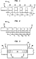
- FIG. 1 is a diagram illustrating a fixed-period segmented waveguide taper.
- FIG. 2 is a diagram illustrating an example implementation of a fixed-gap segmented waveguide taper.
- FIG. 3 is a diagram illustrating an integrated waveguide having a taper at each end and a fiber coupled to each taper.
- FIG. 4 is a diagram illustrating insertion loss as a function of the final gap/period ratio for a fixed-period taper.
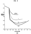
- FIG. 5 is a diagram illustrating insertion loss as a function of the dilution factor for a fixed-gap taper.
- FIGs. 6A and 6B are diagrams illustrating taper length for a fixed-period taper and a fixed-gap taper, respectively.
- FIG. 7 is a diagram illustrating insertion loss as a function of taper length for a fixed-period taper and a fixed-gap taper.
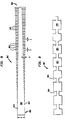
- FIG. 8 is a diagram illustrating an example implementation of a side-gap taper.
- FIG. 9 is an expanded view diagram illustrating an alternate embodiment of the side-gap taper shown in FIG. 8.
- FIG. 10 is a diagram illustrating another embodiment of the side-gap taper of the present invention.
- FIG. 11 is a diagram illustrating another embodiment of the side-gap taper of the present invention.
- FIG. 12 is a diagram illustrating yet another embodiment of the side-gap taper of the present invention.
- FIG. 13 is a diagram illustrating yet another embodiment of the side-gap taper of the present invention.
- the present invention is directed toward a novel approach to implementing a two-dimensional tapered waveguide into integrated-optic devices.
- Two techniques of the invention are described herein, each having multiple embodiments.
- the first technique uses a segmented waveguide, similar to that described above, but with at least one key distinction: the first technique of the present invention implements a fixed-gap, varying-period segmented waveguide.
- the waveguide is not actually segmented in the strict sense of the term.
- gaps are introduced, however, the gaps do not span the entire width of the waveguide. Instead, the gaps, called side-gaps, are cut into the sides of the core of the waveguide and define core sections therebetween.
- the side-gaps are filled with cladding material.
- a depth of each side-gap increases along the iength of the taper. At a first end of the taper, which is adjacent the waveguide, the depth of the notches are relatively small. Whereas the depth of side-gaps on the fiber end of the core are larger.
- the depth of the side-gaps increase (i.e., gradually or in step-like manner) along the taper from the waveguide end to the fiber end as a function of their position along the taper.
- Section 2 of this document discusses the fixed gap segmentation approach, and compares it's results to other segmentation approaches.
- Section 3 discusses the side-gap taper approach.
- the term “length” is used to refer to a dimension in the propagation direction and along a longitudinal axis of waveguide 104; and “width” refers to a dimension orthogonal to the propagation direction and in parallel to the semiconductor and glass layers.
- this document refers to a tapered waveguide. It is within the scope of the invention to have the taper integrated with or coupled to the waveguide.
- FIG. 1 is a diagram illustrating a fixed period segmented taper 100.
- the fixed period segmented taper comprises a waveguide 104 and a plurality of segments 108.
- An optical fiber (not shown) is coupled to the waveguide 104 at a fiber junction 114.
- Each segment 108 comprises a gap portion and a core portion of waveguide material.
- the period ⁇ remains constant or fixed along the propagation direction for the entire length of the taper 100.
- the gap length s of each segment 108 is varied. That is as light travels along the waveguide toward the fiber it encounters increased lengths of gap material. As a result, the effective index difference between the core and the cladding is decreased, causing the mode to expand. Conversely, as light travels from the fiber toward the waveguide it encounters decreasing lengths of gap material ( s ). As a result, the effective index difference is increased causing the mode to be more confined.
- segmented tapers As discussed by Weissman and Hardy. However, Weissman and Hardy discuss applications of such tapers in Rb:KTiOPO 4 waveguides.
- segmented tapers using, for example, Silica-on-Silicon technology
- the inventors have discovered that fixed period (fixed ⁇ ) segmented tapers (i.e., tapers where the gap length s increases with each subsequent gap along the propagation direction) as taught by Weissman and Hardy, result in leakage loss into the substrate. This is primarily due to the properties of the materials used when implementing waveguides using certain materials, such as Silica-on-Silicon technology.
- Waveguides in Silica-on-Silicon technology often use SiO 2 as the cladding material and doped SiO 2 for the core material.
- the waveguide is fabricated on a Silicon substrate.
- the gap material used is also SiO 2 .
- SiO 2 has a refractive index of approximately 1.45
- the Silicon substrate has a refractive index of 3.5. Due to the relative indexes of these materials, total internal reflection is not achieved.
- part of the mode field tail is lost to the substrate. This results in an increased loss.
- This improved taper is a fixed gap-length tapered waveguide. Using a fixed gap length allows the amount of light lost to the substrate to be decreased.
- FIG. 2 is a diagram illustrating a fixed gap length ( s ) segmented taper 200 of the present invention.
- the gap length s of each successive segment is substantially the same.
- the length t of the core portion of each consecutive segment is decreased progressively, thus correspondingly decreasing the period as shown by ⁇ , ⁇ I , ⁇ II , ⁇ III , ⁇ IV , and ⁇ V .
- the leakage loss is minimized from each segment, as will be discussed below.
- Insertion loss is defined as the total signal loss as the light travels from an input fiber to an output fiber and includes leakage loss. Insertion loss is also introduced at the fiber/waveguide junctions 114 due to mode mismatch. Leakage loss, described above, is the loss of light, due primarily to scattering, from the waveguide to the substrate.
- FIG. 3 is a diagram illustrating sources of insertion loss and leakage loss in a waveguide/fiber package.
- waveguide 104 is fabricated in a layer 304, such as glass, or silica, and optical fibers 308 are coupled to either end of waveguide 104 at fiber/waveguide junction 114.
- the fiber ends are cleaved, polished and butt-coupled to waveguide 104.
- a taper shown generally at 312 (which may include fixed period taper 100, fixed gap taper 200 or side-gap taper 802) is used on either end of waveguide 104 to match the mode of waveguide 104 to the mode of the fiber 308. In such a package, leakage loss is introduced by light scattering from the core of the taper 312 into the substrate.
- FIG. 4 is a diagram illustrating the insertion loss (ordinate) characteristics of a fixed period taper 100 as a function of the final ratio of the gap to the period s/(s+t) (abscissa).
- the results illustrated in FIG. 4 are theoretical and are from a study performed by the inventors using light having a wavelength ⁇ of 1.32 ⁇ m (microns) and standard 5-D fiber (d-8 ⁇ m, ⁇ n of 0.39%).
- the core is a 5x5 ⁇ m core with an index ratio ⁇ n of 0.62%.
- An initial gap used is 0.5 ⁇ m.
- the initial gap is the first gap on the waveguide end of the taper.
- the gap increment which is the length by which each consecutive gap is increased along the length of the taper (from waveguide end toward fiber end), is 0.25 ⁇ m.
- FIG. 5 is a graph illustrating the insertion loss of a fixed gap taper 200 according to one embodiment of the invention, namely, the fixed gap taper.
- the gap length s is maintained constant among successive gaps in the fixed gap taper 200.
- FIG. 5 illustrates the insertion loss (ordinate) as a function of a characteristic called the dilution factor (abscissa).
- the dilution factor is a measure of the ratio of the gap length ( s ) over period (s+t) for each segment. Because gap length s remains constant and the period (s+t) decreases along the length of the taper in the direction of the fiber 308, the dilution factor increases with the length of the taper.
- the theoretical results in FIG. 5 were obtained assuming light having a wavelength ⁇ of 1.32 ⁇ m and standard 5-D fiber.
- the core is a 5x5 ⁇ m core with an index ratio ⁇ n of 0.62%.
- the 2 ⁇ m gap length is chosen because it is readily achievable using current fabrication processes, although alternative gap lengths can be chosen.
- the minimum insertion loss occurs where the dilution factor is approximately 0.5.
- the core portion is equal to 2 ⁇ m
- the leakage loss characteristics for a fixed period taper 100 are generally undesirable due to the increasing gap length introduced in the direction from waveguide 104 to fiber 308.
- Another factor affecting leakage loss is the length of the taper. This factor can be an area of concern for both the fixed-period taper 100 and the fixed-gap taper 200.
- the reason taper length is a factor with leakage loss is simple: Due to the increased mode size, the extended mode field tail extends into the substrate and energy is lost. As a result, leakage loss can be a more serious concern in the fixed period taper 100 where total taper length is increased.
- the leakage loss characteristics of fixed period tapers 100 and fixed gap tapers 200 are now described and compared.
- FIGs. 6A and 6B illustrate the concept of mode size expansion for fixed period taper 100 (FIG. 6A) and the fixed gap taper 200 (FIG. 6B).
- the total taper length for the fixed period taper is l FP and for the fixed gap taper is l FG .
- the optimum total taper length of each taper is where the minimum insertion loss occurs, in particular, at the final gap/period ratio shown by the arrow labeled "optimum G/P" in FIG. 7; and the optimum dilution factor shown by the arrow labeled "optimum DF' in FIG. 7.
- the additional length 640 of the taper beyond the optimum total taper length is due to manufacturing error.
- the optimum total taper length is obtained where the dilution factor is approximately 0.5.
- the optimum total taper length associated with the minimum insertion loss can be determined from FIG. 7 and is discussed below.
- a comparison of the optimum total tape lengths ( l FP and l FG ) for the fixed period taper 100 and the fixed gap taper 200 is made at comparable insertion loss points.
- the optimum total taper length is where the s/(s+t), is equal to approximately 0.4, and where the insertion loss is at a minimum of approximately 0.2 dB.
- FIG. 7 which shows the taper length versus insertion loss for a fixed period taper, this corresponds to a taper length l FP of approximately 575 ⁇ m.
- the optimum total taper length l is significantly shorter for the fixed gap taper 200 than can be obtained for the fixed-period taper 100 (e.g., l FG ⁇ 1 ⁇ 2 l FP , as illustrated in FIG. 7).
- the leakage loss is less for the fixed gap taper 200 of the present invention.
- a second embodiment of the waveguide taper has a first end (shown generally at 890 in FIG. 8) for being integrated with or coupled to a waveguide and second end (shown generally at 892 in FIG. 8) for being coupled to a fiber.
- the gaps do not traverse an entire width w of a core 808.
- the gaps do not extend from one outermost side 810 of the core 808 to another outermost side 812 of the core 808.
- side-gaps 804 are cut in the outermost sides (810 and 812) of the core 808 and are filled with cladding material.
- a depth d of the side-gaps 804 may vary from first end 890 to second end 892.
- side-gaps 804 are formed in the outermost sides 810 and 812 for substantially the entire length of the taper 802 from the first end 890 to the second end 892 and extend into core 808 in a direction perpendicular to the direction of light propagation.
- the side-gaps 804 define core segments 805 therebetween.
- the side-gaps 804 extend deeper into the core 808 than at the first end 890.
- the depth d of the side-gaps 804 increases progressively from the first end 890 of the side-gap taper 802 toward the second end 892.
- the outermost sides 810 and 812 of the core 808 are sloped such that the entire width of the core 808 increases toward the second end 892.
- an overall width (between the outermost sides 810 and 812) of the core 808 of the taper 802 may vary from the first end 890 (where mode confinement is at a maximum) to the second end 892 of the taper 802 to further facilitate matching the optical mode of the waveguide with the optical mode of the fiber.
- the width of the second end 892 of the taper 802 may be tailored to correspond to the diameter of the particular fiber to which it will be coupled (at least in one dimension). In particular, with this embodiment, not only the delta ( ⁇ ) between the waveguide and fiber is matched, but also the geometry of the waveguide and fiber are matched.
- the delta of a waveguide or fiber is defined as the fractional differences of the refractive index between the core and the cladding.
- the connection therebetween is improved and losses are reduced.
- the side-gaps 804 may be angled or tilted to reduce back-reflection as will be discussed below with reference to FIG. 9.
- the dilution factor is now: where w is the width of the taper 802, d is the depth of the side-gaps, s is the length (in the light propagation direction) of the side-gaps 804, t is the length of the core section, and f is a weighting factor determined by the magnitude of the optical field in the side-gap 804 relative to that at the center of the taper 802.
- the depth d of the side-gaps 804 thus becomes an additional degree of freedom in controlling the dilution factor DF.
- the overall width of the side-gap taper 802 is also gradually expanded to a size at the second end 892 that is comparable to or larger than the core diameter of the fiber.
- the coupling loss is further reduced because of the improved match of the optical mode between the taper 802 and the fiber.
- the coupling efficiency of the taper 802 is also more tolerant of fabrication errors in the size of the side-gap because with the expanded width of the core 808 of taper 802, it depends less on the dilution ratio.
- one embodiment of the taper 802 may have a width at the first end 890 of 5 ⁇ m and is expanded gradually to 8 ⁇ m at the second end 892.
- the length of the taper 802 is approximately 800 ⁇ m
- the side-gap length s is approximately 4 ⁇ m.
- the side-gap depth d starts at 0 ⁇ m at the first end 890 and increases gradually to 3 ⁇ m at the second end 892.
- the period of the segmentation is approximately 12 ⁇ m.
- the interface between the core portions 805 and side-gaps 804 in taper 802 causes the guided lightwave to reflect.
- this negligible amount of reflection may be strong enough to be intolerable by applications requiring low return loss (i.e., backward reflection). Accordingly, the embodiment of the present invention as shown in FIG. 9 is used.
- a taper 902 is shown having side-gaps 904 and core 908 with core portions 905.
- an interface between the side-gaps 904 and core portions 905 is tilted (randomly here) and aperiodic in position is order to reduce back reflection.
- Side-gaps 904 are configured so that the interface between the side-gaps 904 and the core portions 905 are at an angle of typically 75° (instead of 90° as shown in FIG. 8) relative to the light propagating direction.
- the interface between the side-gaps 904 and core portions 905 are placed at non-periodic positions along the side-gap taper 902 to avoid coherent reflections.
- the aspect ratio in FIG. 9 is 1:1.
- the depth d of side gaps 904 may vary in accordance with the invention.
- FIGs. 10, 11, 12, and 13 show examples of alternate embodiments of the tapers 802 and 902 of the present invention.
- FIG. 10 shows a step-like increase in the width w of the core 1008 of taper 1002 having side gaps 1004 and core portions 1005.
- FIG. 11 shows an alternate embodiment of side-gaps 1104 in a portion of taper 1102 having a triangular configuration.
- FIG. 12 shows an alternate embodiment of side-gaps 1204 in a portion of taper 1202.
- FIG. 13 shows an embodiment of side-gaps 1304 in a portion of taper 1302.
- these embodiments are provided for purposes of illustration only and it is within the scope of the invention to vary the placement, angle, size and orientation of the side-gaps both systematically and randomly for the taper.
- each subsequent side-gap extends slightly farther into the core than did the previous gap.
- This embodiment could be extended to include an embodiment where each subsequent gap extends slightly farther into the substrate and/or as slightly farther into the core.
Landscapes
- Physics & Mathematics (AREA)
- General Physics & Mathematics (AREA)
- Optics & Photonics (AREA)
- Engineering & Computer Science (AREA)
- Microelectronics & Electronic Packaging (AREA)
- Optical Integrated Circuits (AREA)
Applications Claiming Priority (2)
| Application Number | Priority Date | Filing Date | Title |
|---|---|---|---|
| US08/402,266 US5577141A (en) | 1995-03-10 | 1995-03-10 | Two-dimensional segmentation mode tapering for integrated optic waveguides |
| US402266 | 2003-03-28 |
Publications (3)
| Publication Number | Publication Date |
|---|---|
| EP0731366A2 true EP0731366A2 (fr) | 1996-09-11 |
| EP0731366A3 EP0731366A3 (fr) | 1997-01-15 |
| EP0731366B1 EP0731366B1 (fr) | 2001-11-28 |
Family
ID=23591214
Family Applications (1)
| Application Number | Title | Priority Date | Filing Date |
|---|---|---|---|
| EP96301470A Expired - Lifetime EP0731366B1 (fr) | 1995-03-10 | 1996-03-05 | Segmentation bi-dimensionelle d'un guide d'onde intégré pour en adapter le mode à celui d'une fibre |
Country Status (4)
| Country | Link |
|---|---|
| US (1) | US5577141A (fr) |
| EP (1) | EP0731366B1 (fr) |
| JP (1) | JP3153120B2 (fr) |
| DE (1) | DE69617294T2 (fr) |
Cited By (6)
| Publication number | Priority date | Publication date | Assignee | Title |
|---|---|---|---|---|
| FR2770911A1 (fr) * | 1997-11-10 | 1999-05-14 | Univ Bourgogne | Dispositif optique a guide d'ondes pour le transfert d'energie electromagnetique sous forme d'un faisceau de rayonnement |
| FR2830627A1 (fr) * | 2001-10-10 | 2003-04-11 | Centre Nat Rech Scient | Puce optique a guide integre segmente d'adaptation de mode |
| WO2004059354A1 (fr) | 2002-12-26 | 2004-07-15 | Nippon Telegraph And Telephone Corporation | Support de transmission d'ondes et circuit de guide d'ondes |
| EP1324084A3 (fr) * | 2001-12-21 | 2004-10-13 | Agilent Technologies Inc. (a Delaware Corporation) | Procédé et dispositif pour la réduction des pertes optiques d'insertion dans des commutateurs de guides d'onde intégrés |
| EP1555551A1 (fr) * | 2004-01-13 | 2005-07-20 | Lucent Technologies Inc. | Methode et dispositif pour realiser un couplage compact entre une fibre optique et un guide d'onde optique planaire |
| FR2872298A1 (fr) * | 2004-06-24 | 2005-12-30 | Teem Photonics Sa | Transition optimisee d'un guide dans une gaine. |
Families Citing this family (38)
| Publication number | Priority date | Publication date | Assignee | Title |
|---|---|---|---|---|
| KR100189855B1 (ko) * | 1996-11-18 | 1999-06-01 | 윤종용 | 모드 진화 광커플러 및 그 제조방법 |
| US6243517B1 (en) | 1999-11-04 | 2001-06-05 | Sparkolor Corporation | Channel-switched cross-connect |
| US6293688B1 (en) | 1999-11-12 | 2001-09-25 | Sparkolor Corporation | Tapered optical waveguide coupler |
| US6341189B1 (en) | 1999-11-12 | 2002-01-22 | Sparkolor Corporation | Lenticular structure for integrated waveguides |
| JP3941334B2 (ja) * | 2000-04-20 | 2007-07-04 | 株式会社日立製作所 | 光伝送モジュールおよびそれを用いた光通信システム |
| JP3752965B2 (ja) * | 2000-05-26 | 2006-03-08 | 株式会社日立製作所 | 光モジュール |
| JP3766953B2 (ja) | 2000-09-13 | 2006-04-19 | 日本電信電話株式会社 | 光回路 |
| JP3908923B2 (ja) * | 2001-05-01 | 2007-04-25 | 日本電信電話株式会社 | 光部品、光部品の設計方法および光モジュール |
| US6625348B2 (en) | 2001-05-17 | 2003-09-23 | Optron X, Inc. | Programmable delay generator apparatus and associated method |
| US6748125B2 (en) | 2001-05-17 | 2004-06-08 | Sioptical, Inc. | Electronic semiconductor control of light in optical waveguide |
| US6526187B1 (en) | 2001-05-17 | 2003-02-25 | Optronx, Inc. | Polarization control apparatus and associated method |
| US6912330B2 (en) | 2001-05-17 | 2005-06-28 | Sioptical Inc. | Integrated optical/electronic circuits and associated methods of simultaneous generation thereof |
| US6603889B2 (en) | 2001-05-17 | 2003-08-05 | Optronx, Inc. | Optical deflector apparatus and associated method |
| US6891685B2 (en) | 2001-05-17 | 2005-05-10 | Sioptical, Inc. | Anisotropic etching of optical components |
| CA2368945A1 (fr) | 2002-01-21 | 2003-07-21 | Guomin Yu | Dispositif de guide d'ondes optiques a affaiblissement d'insertion peu eleve |
| US6934427B2 (en) | 2002-03-12 | 2005-08-23 | Enablence Holdings Llc | High density integrated optical chip with low index difference waveguide functions |
| US6950581B2 (en) * | 2002-07-22 | 2005-09-27 | Intel Corporation | Optical coupler apparatus and methods having reduced geometry sensitivity |
| US6870987B2 (en) * | 2002-08-20 | 2005-03-22 | Lnl Technologies, Inc. | Embedded mode converter |
| US7245793B2 (en) * | 2002-11-19 | 2007-07-17 | Nippon Telegraph And Telephone Corporation | Optical waveguide circuit |
| US7245803B2 (en) * | 2003-02-11 | 2007-07-17 | Luxtera, Inc. | Optical waveguide grating coupler |
| US7006732B2 (en) * | 2003-03-21 | 2006-02-28 | Luxtera, Inc. | Polarization splitting grating couplers |
| US6934446B2 (en) * | 2003-03-27 | 2005-08-23 | Lucent Technologies Inc. | Optical waveguiding apparatus having reduced crossover losses |
| US7532793B2 (en) * | 2003-07-29 | 2009-05-12 | Intel Corporation | Segmented waveguide coupler |
| US7773836B2 (en) | 2005-12-14 | 2010-08-10 | Luxtera, Inc. | Integrated transceiver with lightpipe coupler |
| EP2511742B1 (fr) | 2004-08-02 | 2019-05-08 | Nippon Telegraph And Telephone Corporation | Circuit de raccordement optique |
| US7680371B2 (en) * | 2007-02-13 | 2010-03-16 | National Research Council Of Canada | Interface device for performing mode transformation in optical waveguides |
| JP2009251176A (ja) * | 2008-04-03 | 2009-10-29 | Nippon Telegr & Teleph Corp <Ntt> | 光信号処理回路 |
| KR101063957B1 (ko) * | 2010-11-02 | 2011-09-08 | 주식회사 피피아이 | 폴리머 삽입형 실리카 광도파로를 이용하는 전반사형 광 스위치 및 그의 제조 방법 |
| JP2011028299A (ja) * | 2010-11-08 | 2011-02-10 | Nippon Telegr & Teleph Corp <Ntt> | 光回路および光信号処理装置 |
| US9829629B2 (en) * | 2015-05-19 | 2017-11-28 | The Royal Institution For The Advancement Of Learning/Mcgill University | Methods and systems relating to optical waveguide tapers |
| US9726821B2 (en) * | 2015-12-01 | 2017-08-08 | Ranovus Inc. | Adiabatic elliptical optical coupler device |
| US9671560B1 (en) * | 2016-03-18 | 2017-06-06 | Lumentum Operations Llc | Angled periodic segmented waveguide for spot size conversion with reduced return loss |
| CN107505675B (zh) * | 2017-09-29 | 2019-09-10 | 武汉光迅科技股份有限公司 | 一种减小切缝附加光损耗的阵列波导光栅及方法 |
| JP7102712B2 (ja) * | 2017-11-27 | 2022-07-20 | 住友ベークライト株式会社 | 光減衰部付き光導波路フィルムおよび光学部品 |
| KR102312608B1 (ko) | 2018-01-15 | 2021-10-18 | 한국전자통신연구원 | 광 도파로 구조체 |
| WO2022013779A1 (fr) * | 2020-07-14 | 2022-01-20 | National Research Council Of Canada | Antenne de guide d'ondes |
| JP7510079B2 (ja) * | 2020-08-03 | 2024-07-03 | 日本電信電話株式会社 | 光回路 |
| US11409040B1 (en) * | 2021-03-23 | 2022-08-09 | Globalfoundries U.S. Inc. | Optical couplers for ridge-to-rib waveguide core transitions |
Family Cites Families (11)
| Publication number | Priority date | Publication date | Assignee | Title |
|---|---|---|---|---|
| US3774987A (en) * | 1972-06-27 | 1973-11-27 | Bell Electric Research Ltd | Coupling of lasers to optical fibres |
| US3948583A (en) * | 1974-12-09 | 1976-04-06 | Bell Telephone Laboratories, Incorporated | Isolation of passive devices and integration with active devices in optical waveguiding circuits |
| US3978426A (en) * | 1975-03-11 | 1976-08-31 | Bell Telephone Laboratories, Incorporated | Heterostructure devices including tapered optical couplers |
| US4678267A (en) * | 1977-11-18 | 1987-07-07 | The United States Of America As Represented By The Secretary Of The Navy | Parabolic optical waveguide horns and design thereof |
| US4159452A (en) * | 1978-01-13 | 1979-06-26 | Bell Telephone Laboratories, Incorporated | Dual beam double cavity heterostructure laser with branching output waveguides |
| EP0383627B1 (fr) * | 1989-02-17 | 1996-05-08 | Sharp Kabushiki Kaisha | Coupleur à réseau |
| US5074633A (en) * | 1990-08-03 | 1991-12-24 | At&T Bell Laboratories | Optical communication system comprising a fiber amplifier |
| US5212758A (en) * | 1992-04-10 | 1993-05-18 | At&T Bell Laboratories | Planar lens and low order array multiplexer |
| US5265177A (en) * | 1992-05-08 | 1993-11-23 | At&T Bell Laboratories | Integrated optical package for coupling optical fibers to devices with asymmetric light beams |
| US5349602A (en) * | 1993-03-15 | 1994-09-20 | Sdl, Inc. | Broad-area MOPA device with leaky waveguide beam expander |
| US5343542A (en) * | 1993-04-22 | 1994-08-30 | International Business Machines Corporation | Tapered fabry-perot waveguide optical demultiplexer |
-
1995
- 1995-03-10 US US08/402,266 patent/US5577141A/en not_active Expired - Lifetime
-
1996
- 1996-03-05 EP EP96301470A patent/EP0731366B1/fr not_active Expired - Lifetime
- 1996-03-05 DE DE69617294T patent/DE69617294T2/de not_active Expired - Lifetime
- 1996-03-11 JP JP05289096A patent/JP3153120B2/ja not_active Expired - Fee Related
Non-Patent Citations (4)
| Title |
|---|
| ELECTRONICS LETTERS, vol. 28, no. 16, 30 July 1992, pages 1514-1516, XP002017192 WEISSMAN ET AL: "2-D MODE TAPERING VIA TAPERED CHANNEL WAVEGUIDE SEGMENTATION" * |
| ELECTRONICS LETTERS, vol. 31, no. 3, 2 February 1995, page 186/187 XP000504202 NIR D ET AL: "PROTON-EXCHANGED PERIODICALLY SEGMENTED CHANNEL WAVEGUIDES IN LITHIUM NIOBATE" * |
| JOURNAL OF LIGHTWAVE TECHNOLOGY, vol. 11, no. 11, November 1993, pages 1831-1838, XP002017190 WEISSMAN ET AL: "MODES OF PERIODICALLY SEGMENTED WAVEGUIDES" * |
| OPTICS LETTERS, vol. 19, no. 21, 1 November 1994, pages 1732-1734, XP002017191 WEISSMAN ET AL: "PERIODICALLY SEGMENTED WAVEGUIDES IN Ti:LiNbO3" * |
Cited By (10)
| Publication number | Priority date | Publication date | Assignee | Title |
|---|---|---|---|---|
| FR2770911A1 (fr) * | 1997-11-10 | 1999-05-14 | Univ Bourgogne | Dispositif optique a guide d'ondes pour le transfert d'energie electromagnetique sous forme d'un faisceau de rayonnement |
| WO1999024853A1 (fr) * | 1997-11-10 | 1999-05-20 | Universite De Bourgogne | Dispositif optique a guide d'ondes pour le transfert d'energie electromagnetique sous forme d'un faisceau de rayonnement |
| FR2830627A1 (fr) * | 2001-10-10 | 2003-04-11 | Centre Nat Rech Scient | Puce optique a guide integre segmente d'adaptation de mode |
| WO2003032041A3 (fr) * | 2001-10-10 | 2004-01-22 | Centre Nat Rech Scient | Puce optique a guide integre segmente d'adaptation de mode |
| EP1324084A3 (fr) * | 2001-12-21 | 2004-10-13 | Agilent Technologies Inc. (a Delaware Corporation) | Procédé et dispositif pour la réduction des pertes optiques d'insertion dans des commutateurs de guides d'onde intégrés |
| WO2004059354A1 (fr) | 2002-12-26 | 2004-07-15 | Nippon Telegraph And Telephone Corporation | Support de transmission d'ondes et circuit de guide d'ondes |
| EP1577687B1 (fr) * | 2002-12-26 | 2015-05-06 | Nippon Telegraph And Telephone Corporation | Support de transmission d'ondes et circuit de guide d'ondes |
| EP1555551A1 (fr) * | 2004-01-13 | 2005-07-20 | Lucent Technologies Inc. | Methode et dispositif pour realiser un couplage compact entre une fibre optique et un guide d'onde optique planaire |
| FR2872298A1 (fr) * | 2004-06-24 | 2005-12-30 | Teem Photonics Sa | Transition optimisee d'un guide dans une gaine. |
| WO2006090028A1 (fr) * | 2004-06-24 | 2006-08-31 | Teem Photonics | Transition optimisee d'un guide dans une gaine |
Also Published As
| Publication number | Publication date |
|---|---|
| DE69617294T2 (de) | 2002-07-18 |
| US5577141A (en) | 1996-11-19 |
| DE69617294D1 (de) | 2002-01-10 |
| EP0731366B1 (fr) | 2001-11-28 |
| EP0731366A3 (fr) | 1997-01-15 |
| JPH08262245A (ja) | 1996-10-11 |
| JP3153120B2 (ja) | 2001-04-03 |
Similar Documents
| Publication | Publication Date | Title |
|---|---|---|
| US5577141A (en) | Two-dimensional segmentation mode tapering for integrated optic waveguides | |
| EP0731367B1 (fr) | Guide d'onde optique intégré avec des encoches latérales pour en adapter le mode à celui d'un fibre | |
| US4737004A (en) | Expanded end optical fiber and associated coupling arrangements | |
| US7013067B2 (en) | Silicon nanotaper couplers and mode-matching devices | |
| US4715672A (en) | Optical waveguide utilizing an antiresonant layered structure | |
| Takato et al. | Low-loss high-silica single-mode channel waveguides | |
| EP0484878B1 (fr) | Circuit optique de branchement en Y | |
| EP1555551B1 (fr) | Dispositif pour realiser un couplage compact entre une fibre optique et un guide d'onde optique planaire | |
| US12313882B2 (en) | Taper-based spot-size converter implementing intermediate optical mode converter | |
| EP0220315B1 (fr) | Dispositifs comprenant des guides d'ondes optiques a perte faible | |
| CN1922520A (zh) | 包括两级接续器的模尺寸转换器 | |
| JP3175814B2 (ja) | 導波形光素子及びその製造方法 | |
| JP2850996B2 (ja) | 光結合デバイス | |
| JP3084417B2 (ja) | 光結合デバイス | |
| US7035508B2 (en) | Waveguide structure having improved reflective mirror features | |
| Baba et al. | A novel 3-dimensional ARROW by thin film patterning—Stripe lateral confinement of ARROW— | |
| WO2004061507A1 (fr) | Coupleur de dispositif semi-conducteur a guide d'onde | |
| CAI et al. | Fiber-waveguide coupler having a linear-tapered form | |
| Nolting | Theoretical investigations of optical waveguide tapers on InGaAsP/lnP | |
| Chen et al. | Vertical tapered mode size transformer in polymer waveguides for efficient fiber coupling | |
| Khilo et al. | Efficient planar single-mode fiber-to-chip coupler based on two-stage adiabatic evolution | |
| Sakurai et al. | Modeling of a low-loss spot-size converter for hollow waveguides with sub-wavelength air core | |
| Ii et al. | Depressed cladding single-mode fibres for 1300 nm operation | |
| Ramadan | An efficient approach to minimize radiation loss at index discontinuities of optical waveguides | |
| Guha et al. | Design of a multimode fixed optical coupler using simplified formula |
Legal Events
| Date | Code | Title | Description |
|---|---|---|---|
| PUAI | Public reference made under article 153(3) epc to a published international application that has entered the european phase |
Free format text: ORIGINAL CODE: 0009012 |
|
| AK | Designated contracting states |
Kind code of ref document: A2 Designated state(s): DE FR GB |
|
| PUAL | Search report despatched |
Free format text: ORIGINAL CODE: 0009013 |
|
| AK | Designated contracting states |
Kind code of ref document: A3 Designated state(s): DE FR GB |
|
| 17P | Request for examination filed |
Effective date: 19970701 |
|
| 17Q | First examination report despatched |
Effective date: 19971009 |
|
| GRAG | Despatch of communication of intention to grant |
Free format text: ORIGINAL CODE: EPIDOS AGRA |
|
| GRAG | Despatch of communication of intention to grant |
Free format text: ORIGINAL CODE: EPIDOS AGRA |
|
| GRAG | Despatch of communication of intention to grant |
Free format text: ORIGINAL CODE: EPIDOS AGRA |
|
| GRAH | Despatch of communication of intention to grant a patent |
Free format text: ORIGINAL CODE: EPIDOS IGRA |
|
| GRAH | Despatch of communication of intention to grant a patent |
Free format text: ORIGINAL CODE: EPIDOS IGRA |
|
| GRAA | (expected) grant |
Free format text: ORIGINAL CODE: 0009210 |
|
| AK | Designated contracting states |
Kind code of ref document: B1 Designated state(s): DE FR GB |
|
| REG | Reference to a national code |
Ref country code: GB Ref legal event code: IF02 |
|
| REF | Corresponds to: |
Ref document number: 69617294 Country of ref document: DE Date of ref document: 20020110 |
|
| ET | Fr: translation filed | ||
| PLBE | No opposition filed within time limit |
Free format text: ORIGINAL CODE: 0009261 |
|
| STAA | Information on the status of an ep patent application or granted ep patent |
Free format text: STATUS: NO OPPOSITION FILED WITHIN TIME LIMIT |
|
| 26N | No opposition filed | ||
| PGFP | Annual fee paid to national office [announced via postgrant information from national office to epo] |
Ref country code: FR Payment date: 20140311 Year of fee payment: 19 |
|
| PGFP | Annual fee paid to national office [announced via postgrant information from national office to epo] |
Ref country code: GB Payment date: 20140305 Year of fee payment: 19 |
|
| PGFP | Annual fee paid to national office [announced via postgrant information from national office to epo] |
Ref country code: DE Payment date: 20140417 Year of fee payment: 19 |
|
| REG | Reference to a national code |
Ref country code: DE Ref legal event code: R119 Ref document number: 69617294 Country of ref document: DE |
|
| GBPC | Gb: european patent ceased through non-payment of renewal fee |
Effective date: 20150305 |
|
| REG | Reference to a national code |
Ref country code: FR Ref legal event code: ST Effective date: 20151130 |
|
| PG25 | Lapsed in a contracting state [announced via postgrant information from national office to epo] |
Ref country code: GB Free format text: LAPSE BECAUSE OF NON-PAYMENT OF DUE FEES Effective date: 20150305 Ref country code: DE Free format text: LAPSE BECAUSE OF NON-PAYMENT OF DUE FEES Effective date: 20151001 |
|
| PG25 | Lapsed in a contracting state [announced via postgrant information from national office to epo] |
Ref country code: FR Free format text: LAPSE BECAUSE OF NON-PAYMENT OF DUE FEES Effective date: 20150331 |