EP0731424A1 - Appareil pour éliminer les surfaces cachées avec tampon de profondeur - Google Patents
Appareil pour éliminer les surfaces cachées avec tampon de profondeur Download PDFInfo
- Publication number
- EP0731424A1 EP0731424A1 EP95304022A EP95304022A EP0731424A1 EP 0731424 A1 EP0731424 A1 EP 0731424A1 EP 95304022 A EP95304022 A EP 95304022A EP 95304022 A EP95304022 A EP 95304022A EP 0731424 A1 EP0731424 A1 EP 0731424A1
- Authority
- EP
- European Patent Office
- Prior art keywords
- data
- input
- buffer
- value
- output
- Prior art date
- Legal status (The legal status is an assumption and is not a legal conclusion. Google has not performed a legal analysis and makes no representation as to the accuracy of the status listed.)
- Granted
Links
Images





Classifications
-
- G—PHYSICS
- G06—COMPUTING OR CALCULATING; COUNTING
- G06T—IMAGE DATA PROCESSING OR GENERATION, IN GENERAL
- G06T15/00—Three-dimensional [3D] image rendering
- G06T15/10—Geometric effects
- G06T15/40—Hidden part removal
- G06T15/405—Hidden part removal using Z-buffer
Definitions
- the present invention relates to a Z buffer hidden surface removal device (HSRD), and more particularly to a hidden surface removal device that uses the depth information (Z data) of an object drawn in a three-dimensional or two-dimensional image display device to perform hidden surface removal by a Z buffer.
- HSRD Z buffer hidden surface removal device
- a conventional graphic engine usually has a frame buffer and a Z buffer.
- the frame buffer serves as a memory for holding the digital expressions of the color and brightness of each pixel within an image, such as a dynamic random access memory (DRAM) or a static random access memory (SRAM).
- the Z buffer serves as a memory for holding a numeral for each pixel within the frame buffer.
- the numeral stored in this Z buffer is called Z data or a Z value and is depth information representative of the distance between an observer and an object displayed with pixels. Smaller Z data indicates that the object is closer to the observer.
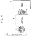
- a conventional Z buffer HSRD comprises an input-output portion 1 for performing input-output of data such as a Z value, a counter value, and an address, with the outside, a Z buffer portion 2 for storing a Z value, and a Z operation circuit portion 6 for inputting the Z value and outputting a write control signal and an operation result.
- step S101 two data of Z data (Zs) and a write address (Adr) are read out from the input-output portion 1 (step S101).
- Z data (Zd) being currently stored in an address (Adr) within the Z buffer portion 2 is taken out of the Z buffer portion 2 (step S102).
- the Z data (Zs) from the input-output portion 1 and the Z data (Zd) taken out of the Z buffer portion 2 are compared (step S103).
- step S104 When the Z data (Zs) is smaller (step S104), i.e., when a desired pixel is on the side closer to the observer, a "1" is output as a write control signal (step S105).
- This write control signal is also used in the writing to the Z buffer portion 2, and in the case of "1," the Z data (Zs) from the input-output portion 1 is written to the position of the address (Adr) of the Z buffer portion 2 (step S106). Also, when it is determined in the step S104 that Zd is smaller than Zs, a "0" is output as a write control signal (step S107), and in this case, nothing is written to the Z buffer portion 2.
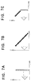
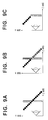
- FIGS. 7A to 7C show ideal hidden surface removal processes.
- the right direction represents a Z-axis direction and the arrow represents a direction in which an observer is seeing.
- FIG. 7A shows data written first
- FIG. 7B shows data that is newly written with respect to the first data.
- FIG. 7C shows a result in which ideal hidden surface removal was accomplished by overlapping two pixel data. Thus, only pixels close to the view point of the observer remain.
- FIGS. 8A to 8C show the results obtained as data was written in the same method as a write method of normal memories.
- data is always overwritten. If data is written over the first data of FIG. 8A, the result will become as shown in FIG. 8B. As a result, since data written later always remains as shown in FIG. 8C, consequently, hidden surface removal will not be performed correctly.
- FIGS. 9A to 9C show the processes of removing a hidden surface by a conventional Z buffer method. If data to be written is laid over the data of FIG. 9A, the result will become as shown in FIG. 9B. If greater Z data is not written like the crosshatched pixels of FIG. 9B or if it is overwritten by other Z data, then it does not remain in the Z buffer. Among Z data finally written in all addresses of the Z buffer, the smallest data remains as shown in FIG. 9C.
- the hidden surface removal is performed in this way, and what is output from the conventional Z buffer HSRD is a write control signal representative of the possibility and impossibility of writing for each data, and Z data that finally remained within the Z buffer.
- the Z data of the above-described HSRD is insufficient in applications such as virtual reality in which an image of high picture quality needs to be generated with real time.
- FIG. 10A illustrates the sun appearing from behind the cloud and the glow generated around it.
- the light passing through the eyelashes is diffracted and radial rays generate around the object.
- an image of the cloud is drawn with a certain Z value, as shown in FIG. 10B, and then an image of the sun is drawn with a greater Z value than that, as shown in FIG. 10C. Finally an image of the glow is drawn with a Z value smaller than the cloud.
- ideal hidden surface removal is performed, there is no possibility that a pixel being in a longer distance is written over a pixel being in a shorter distance, so there is no possibility that the image of the sun is written over the image of the cloud. Therefore, a result like FIG. 10C is obtained.
- the lightness of the sun can be approximated with constant times the visual field area of the sun not hidden by other object, i.e., the uncovered visual field area of the sun.
- the uncovered visual field area can be obtained in the process of the hidden surface removal. First, all objects that can become an obstacle are drawn, and finally the image of the sun is drawn. If the number of pixels that were hidden-surface removed is subtracted from the number of pixels of the image of the sun, the number of uncovered pixels of the sun will be obtained.
- the hidden surface removal is performed as described above, but what is output from the conventional Z buffer HSRD was binary data indicating that the pixel having the Z value can be drawn to the frame buffer or the pixel having the Z value cannot be drawn to the frame buffer.
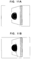
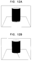
- FIGS. 11A, 11B and FIGS. 12A and 12B are examples of the case where binary hidden surface removal is insufficient.
- FIGS. 11A and 11B which are a first example is a case where an object whose outline is dim and which projects from a wall is drawn.
- the object it is preferable that the object be drawn so that it becomes transparent as it comes closer to the wall.
- a boundary line between the object and the wall indicated by the arrow of FIG. 11B, becomes clear and the dim feeling of the object disappears.
- FIGS. 12A and 12B which are a second example is a case where an object projecting from muddy water is drawn.
- the water around the object projecting from muddy water be transparent.
- a boundary line between the object and the wall becomes clear and the transparent feeling of water disappears, as shown in FIG. 12B.
- the image of the sun when the image of the sun is sufficiently large, it can be used as an uncovered visual field area of the sun, but since the conventional Z buffer HSRD outputs only a write control signal representative of the possibility or impossibility of writing for each data, and Z data that finally remained in the Z buffer, the above-described number of uncovered visual field pixels and number of pixels to be drawn could not be provided to an observer. Therefore, the number of uncovered visual field pixels and the number of pixels to be drawn, which are used when the lightness of the sun appearing from behind the cloud is calculated, cannot be output.
- the conventional HSRD outputs a result of a Z operation only as binary data indicating that a pixel with the Z value can be drawn to the frame buffer or a pixel with the Z value cannot be drawn to the frame buffer, sufficient information cannot be provided when an object whose lightness changes according to the distance and thickness is drawn.
- An object of the present invention is to provide a Z buffer hidden surface removal device (HSRD) which is capable of overcoming the above-described problems, calculating the lightness of the sun appearing from behind the cloud without increasing the capacity of a memory, and displaying an image with far and near feelings by deciding whether two planes cross each other nor not.
- HSRD Z buffer hidden surface removal device
- a hidden surface removal device comprising: Z buffer means for storing a Z value of each of pixels to be displayed; input-output means for inputting and outputting data such as a Z value, a counter value, and an address; a Z operation circuit means which uses said Z value input for each pixel by said input-output means and said Z value stored in said buffer means to perform a Z operation and which, according to a result of said Z operation, outputs a write control signal to said input-output means and also outputs the Z operation result to said input-output means; and Z count means for counting a number of pixels matching with a predetermined condition, based on said Z operation result.
- a Z operation between a Z value input for each pixel and a Z value stored in the Z buffer means is performed by the Z operation circuit means, and a number of pixels matching a result of the Z operation is counted by the Z count means.
- a hidden surface removal device comprising: Z buffer means for storing a Z value of each of pixels to be displayed; input-output means for inputting and outputting data such as a Z value, an Opacity value, and an address; a Z operation circuit means which uses said Z value input for each pixel by said input-output means and said Z value stored in said buffer means to perform a Z operation and which, according to a result of said Z operation, outputs a write control signal to said input-output means and also outputs the Z operation result to said input-output means; and means for changing said Opacity value based on said Z operation result.
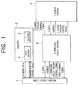
- the Z buffer HSRD of this embodiment comprises an input-output portion 1 as input-output means for inputting Z data, an address, and counter data, from the outside and for outputting counter data, Z data, and a write control signal, to the outside.
- the Z buffer HSRD further comprises a Z buffer portion 2 as Z buffer means in which reading and writing of Z data are performed according to a given Z buffer address and a given Z buffer portion control signal, a Z operation circuit portion 6 as Z operation circuit means for inputting a Z value and outputting a write control signal and an operation result, and a counter portion 3 as Z count means for counting a number of Z data in which, among data that were input to the Z operation circuit portion 6, a result of the Z operation circuit portion 6 matches with predetermined conditions.
- the counter portion 3 consists of a data number counter 4 and a Z counter 5, and can input or output the values of the respective counters from or to the input-output portion 1.
- the data number counter 4 and Z counter 5 of the counter portion 3 are controlled by a counter control signal from the Z operation circuit portion 6.
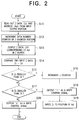
- the Z operation circuit portion 6 If data is input from the outside to the input-output portion 1, it will inform the Z operation circuit portion 6 that an address (Adr) and Z data (Zs) arrived, with the Z operation circuit portion control signal.
- the Z operation circuit portion 6 reads out the address (Adr) and the Z data (Zs) (step S11) and at the same time outputs an increment request to the data number counter 4 with the counter control signal.
- the counter portion 3 then receives this request and the data number counter 4 is incremented (step S12).
- the Z operation circuit portion 6 supplies the address (Adr) to the Z buffer portion 2, and outputs an output request to the Z buffer portion 2 through the Z buffer portion control signal.
- the Z buffer portion 2 In response to the Z buffer portion control signal, the Z buffer portion 2 outputs Z data (Zd) stored in the position of the address (Adr) (step S13).
- the Z data (Zs) input from the Z buffer portion 2 and the Z data (Zd) input from the input-output portion 1 are compared by the Z operation circuit portion 6 (step S14).
- step S15 With the Z operation circuit portion control signal input from the input-output portion 1, it is determined, as a first condition for comparing Z data, if Zs is smaller than Zd (step S15). When Zs is smaller than Zd, a request to increment the Z counter 5 is output with the counter control signal and the Z counter 5 is incremented (step S16). Then, when the comparison result matches with a second condition determined by the Z operation circuit portion control signal that was input from the input-output portion 1 (step S17), the write control signal goes to a "1" (step S18).
- the Z data Zs and the address Adr are output to the Z buffer portion 2, a write request is made with the Z buffer portion control signal, and according to that request, the Z buffer portion 2 stores the Z data Zs in the position corresponding to that address (step S19).
- Zs is not smaller than Zd
- the write operation is not performed in the Z buffer portion 2.
- the write control signal goes to a "0" (step S20).
- the Z operation circuit portion 6 outputs the write control signal to the outside through the input-output portion 1 and then becomes in a new data waiting state. The operation described above will be repeated.
- the input-output portion 1 will output the counter portion control signal to the counter portion 3 to request resetting. Either or both of the data number counter 4 and the Z counter 5 is reset according to the reset request by the counter portion 3. Thereafter, if a request to output Z data is made from the outside, the input-output portion 1 will output the address to the Z operation circuit portion 6 and also output a transfer request of the Z data to the circuit portion 6 with the Z operation circuit portion control signal. According to the request, the Z operation circuit portion 6 outputs the address to the Z buffer portion 2 and also requests the output of the Z data with the Z buffer control signal. According to the output request, the Z buffer portion 2 outputs Z data corresponding to the address.
- the Z operation circuit portion 6 receives the Z data and outputs it to the input-output portion 1.
- the Z data received by the input-output portion 1 is output to the outside. If an output request of a counter value is made from the outside, the input-output portion 1 will send the counter portion control signal to the counter portion 3 to request the counter portion 3 to output a counter value. According to the output request, the counter portion 3 outputs the value of the Z counter 5 or data number counter 4 to the input-output portion 1.
- the counter value received by the input-output portion 1 is output to the outside.
- the Z buffer HSRD of this embodiment comprises an input-output portion 1 for inputting Z data, an address, and an Opacity value A, from the outside and for outputting an Opacity value A, Z data, and a write control signal, to the outside.
- the Z buffer HSRD further comprises a Z buffer portion 2 in which reading and writing of Z data are performed according to a given Z buffer address and a given Z buffer portion control signal, an A modulator portion 3a to which an Opacity value A and an A modulator portion control signal from the input-output portion 1 are input and which changes and outputs the Opacity value A according to the A modulator portion control signal, and a Z operation circuit portion 6 to which a Z value and an address are input and which performs an operation in response to the Z operation circuit control portion control signal.
- the Z operation circuit portion 6 If data is input from the outside to the input-output portion 1, it will inform the Z operation circuit portion 6 that an address and Z data (Zs) arrived, with the Z operation circuit portion control signal.
- the Z operation circuit portion 6 reads out the address and the Z data (step S21) and at the same time outputs an increment request to the data number counter with the counter control signal.
- the Z operation circuit portion 6 supplies the address to the Z buffer portion 2, and outputs an output request to the Z buffer portion 2 through the Z buffer portion control signal. According to the Z buffer portion control signal, the Z buffer portion 2 outputs Z data stored in the position of the address (step S22).
- the Z data (Zd) input from the Z buffer portion 2 and the Z data (Zs) input from the input-output portion 1 are compared by the Z operation circuit portion 6 (step S23).
- a "1" is output as a write control signal (step S25).
- the Z data Zs and the address Adr are output to the Z buffer portion 2, a write request is made with the Z buffer portion control signal, and according to that request, the Z buffer portion 2 stores the Z data Zs in the position corresponding to the address (step S26).
- a "0" is output as a write control signal (step S27) and the write operation is not performed in the Z buffer portion 2.
- the write control signal is output to the outside through the input-output portion 1.
- the Z operation circuit portion 6 subtracts Zd from Zs according to an operation method that is determined by the Z operation circuit portion control signal from the input-output portion 1 (step S28), and the result is output as a Z operation result (Zam) to the A modulator portion 3.
- the Zam and the Opacity value A are calculated according to an operation method that is determined by the A modulator portion control signal from the input-output portion 1, and the result is output as an Opacity value A to the input-output portion 1 (step S29).
- the Opacity value A is output to the outside through the input-output portion 1. Then, the Z operation circuit portion 6 will be in a new data waiting state.
- the input-output portion 1 will output the address to the Z operation circuit portion 6 and also output a transfer request of the Z data through a Z operation circuit portion signal.
- the Z operation circuit portion 6 outputs the address to the Z buffer portion 2 and also requests the output of the Z data with the Z buffer control signal.
- the Z buffer portion 2 outputs the Z data corresponding to the address.
- the Z operation circuit portion 6 receives the Z data and outputs it to the input-output portion 1.
- the Z data received by the input-output portion 1 is output to the outside.
Landscapes
- Physics & Mathematics (AREA)
- Engineering & Computer Science (AREA)
- Geometry (AREA)
- Computer Graphics (AREA)
- General Physics & Mathematics (AREA)
- Theoretical Computer Science (AREA)
- Image Generation (AREA)
Applications Claiming Priority (3)
| Application Number | Priority Date | Filing Date | Title |
|---|---|---|---|
| JP7049799A JPH08249494A (ja) | 1995-03-09 | 1995-03-09 | Zバッファ方式隠面消去装置 |
| JP49799/95 | 1995-03-09 | ||
| JP4979995 | 1995-03-09 |
Publications (2)
| Publication Number | Publication Date |
|---|---|
| EP0731424A1 true EP0731424A1 (fr) | 1996-09-11 |
| EP0731424B1 EP0731424B1 (fr) | 2001-11-14 |
Family
ID=12841202
Family Applications (1)
| Application Number | Title | Priority Date | Filing Date |
|---|---|---|---|
| EP95304022A Expired - Lifetime EP0731424B1 (fr) | 1995-03-09 | 1995-06-09 | Appareil pour éliminer les surfaces cachées avec tampon de profondeur |
Country Status (4)
| Country | Link |
|---|---|
| US (1) | US5896134A (fr) |
| EP (1) | EP0731424B1 (fr) |
| JP (1) | JPH08249494A (fr) |
| DE (1) | DE69523890T2 (fr) |
Cited By (3)
| Publication number | Priority date | Publication date | Assignee | Title |
|---|---|---|---|---|
| WO2001022369A1 (fr) * | 1999-09-17 | 2001-03-29 | Imagination Technologies Limited | Mixage base sur la profondeur pour systemes graphiques en 3d |
| CN100541539C (zh) * | 2005-02-24 | 2009-09-16 | 株式会社东芝 | 用于执行隐藏面消除的设备和方法 |
| US9489767B1 (en) | 2007-12-13 | 2016-11-08 | Nvidia Corporation | Cull streams for fine-grained rendering predication |
Families Citing this family (3)
| Publication number | Priority date | Publication date | Assignee | Title |
|---|---|---|---|---|
| JP3765931B2 (ja) * | 1998-10-15 | 2006-04-12 | 富士通株式会社 | バッファ制御方法及びバッファ制御装置 |
| US20030063087A1 (en) * | 2001-09-28 | 2003-04-03 | Doyle Peter L. | Variable-formatable width buffer and method of use |
| US8081182B2 (en) * | 2004-03-03 | 2011-12-20 | Qualcomm Incorporated | Depth buffer for rasterization pipeline |
Citations (4)
| Publication number | Priority date | Publication date | Assignee | Title |
|---|---|---|---|---|
| EP0379983A2 (fr) * | 1989-01-23 | 1990-08-01 | Honeywell Inc. | Commande d'interface mémoire |
| WO1991018359A1 (fr) * | 1990-05-12 | 1991-11-28 | Rediffusion Simulation Limited | Generateur d'images |
| EP0527587A2 (fr) * | 1991-08-08 | 1993-02-17 | Bolt Beranek And Newman Inc. | Traitement de pixel à effets volumétriques |
| EP0553973A2 (fr) * | 1992-01-29 | 1993-08-04 | International Business Machines Corporation | Méthode d'affichage graphique à calculateur et système avec génération d'ombre |
Family Cites Families (7)
| Publication number | Priority date | Publication date | Assignee | Title |
|---|---|---|---|---|
| US4951232A (en) * | 1988-09-12 | 1990-08-21 | Silicon Graphics, Inc. | Method for updating pipelined, single port Z-buffer by segments on a scan line |
| US5490238A (en) * | 1990-03-19 | 1996-02-06 | Evans & Sutherland Computer Corporation | Attribute blending system for composing computer-graphic images from objects |
| US5265199A (en) * | 1991-05-22 | 1993-11-23 | Silicon Graphics, Inc. | Method and apparatus for accomplishing Z-buffering by prediction |
| TW241196B (fr) * | 1993-01-15 | 1995-02-21 | Du Pont | |
| US5583974A (en) * | 1993-05-10 | 1996-12-10 | Apple Computer, Inc. | Computer graphics system having high performance multiple layer Z-buffer |
| US5528738A (en) * | 1993-10-06 | 1996-06-18 | Silicon Graphics, Inc. | Method and apparatus for antialiasing raster scanned, polygonal shaped images |
| US5526471A (en) * | 1993-12-15 | 1996-06-11 | International Business Machines Corporation | Rendering of non-opaque media using the p-buffer to account for polarization parameters |
-
1995
- 1995-03-09 JP JP7049799A patent/JPH08249494A/ja active Pending
- 1995-06-09 EP EP95304022A patent/EP0731424B1/fr not_active Expired - Lifetime
- 1995-06-09 DE DE69523890T patent/DE69523890T2/de not_active Expired - Lifetime
-
1997
- 1997-11-21 US US08/976,075 patent/US5896134A/en not_active Expired - Lifetime
Patent Citations (4)
| Publication number | Priority date | Publication date | Assignee | Title |
|---|---|---|---|---|
| EP0379983A2 (fr) * | 1989-01-23 | 1990-08-01 | Honeywell Inc. | Commande d'interface mémoire |
| WO1991018359A1 (fr) * | 1990-05-12 | 1991-11-28 | Rediffusion Simulation Limited | Generateur d'images |
| EP0527587A2 (fr) * | 1991-08-08 | 1993-02-17 | Bolt Beranek And Newman Inc. | Traitement de pixel à effets volumétriques |
| EP0553973A2 (fr) * | 1992-01-29 | 1993-08-04 | International Business Machines Corporation | Méthode d'affichage graphique à calculateur et système avec génération d'ombre |
Cited By (4)
| Publication number | Priority date | Publication date | Assignee | Title |
|---|---|---|---|---|
| WO2001022369A1 (fr) * | 1999-09-17 | 2001-03-29 | Imagination Technologies Limited | Mixage base sur la profondeur pour systemes graphiques en 3d |
| US6809730B2 (en) | 1999-09-17 | 2004-10-26 | Imagination Technologies Limited | Depth based blending for 3D graphics systems |
| CN100541539C (zh) * | 2005-02-24 | 2009-09-16 | 株式会社东芝 | 用于执行隐藏面消除的设备和方法 |
| US9489767B1 (en) | 2007-12-13 | 2016-11-08 | Nvidia Corporation | Cull streams for fine-grained rendering predication |
Also Published As
| Publication number | Publication date |
|---|---|
| JPH08249494A (ja) | 1996-09-27 |
| DE69523890T2 (de) | 2002-07-04 |
| US5896134A (en) | 1999-04-20 |
| EP0731424B1 (fr) | 2001-11-14 |
| DE69523890D1 (de) | 2001-12-20 |
Similar Documents
| Publication | Publication Date | Title |
|---|---|---|
| CA2289478C (fr) | Orientation d'images parametrees pour ecrans d'ordinateurs | |
| TW459208B (en) | Method of and apparatus for processing image, recording medium, and program | |
| JP3761085B2 (ja) | 画像処理装置及びその構成部品、レンダリング処理方法 | |
| US5570433A (en) | Apparatus and method for defocusing images | |
| US4855938A (en) | Hidden line removal method with modified depth buffer | |
| US4924414A (en) | Apparatus and method for obtaining priority numbers for drawing figures forming a display figure | |
| EP0740272A2 (fr) | Procédé et dispositif pour représenter rapidement une image à trois dimensions | |
| EP0780798A2 (fr) | Procédé et appareil pour l'identification d'objets et la détection de collisions dans un espace graphique tridimensionnel | |
| EP1214689B1 (fr) | Procede et dispositif permettant de rendre une image avec refraction | |
| JPS6380375A (ja) | テクスチヤマツピング装置 | |
| US5896134A (en) | Z buffer hidden surface removal device | |
| JPH02178785A (ja) | 立体表示方法およびその装置 | |
| JP3629243B2 (ja) | モデリング時の距離成分を用いてレンダリング陰影処理を行う画像処理装置とその方法 | |
| US20080211811A1 (en) | Drawing Apparatus for Displaying Image Data About a Plurality of Objects Including Semitransparent Object and Opaque Object on Computer Display Screen | |
| KR100429092B1 (ko) | 그래픽영상처리방법및장치 | |
| JPH07182526A (ja) | グラフィックス表示装置の表示方法 | |
| EP0589724B1 (fr) | Système et méthode électronique de traitement d'images | |
| CA1205201A (fr) | Appareil de traitement de donnees de configuration | |
| EP0538057B1 (fr) | Systèmes électroniques graphiques | |
| US6992678B2 (en) | Image processing apparatus and method of same | |
| JP3272463B2 (ja) | 画像作成装置およびその使用方法 | |
| JP4482996B2 (ja) | データ記憶装置とその方法および画像処理装置 | |
| US6088033A (en) | Method and apparatus for processing picture elements | |
| US20030071827A1 (en) | Anti-aliasing method with z-merge | |
| US20020089509A1 (en) | Memory device having depth compare-write function and method for depth compare-write used by the memory device |
Legal Events
| Date | Code | Title | Description |
|---|---|---|---|
| PUAI | Public reference made under article 153(3) epc to a published international application that has entered the european phase |
Free format text: ORIGINAL CODE: 0009012 |
|
| 17P | Request for examination filed |
Effective date: 19960419 |
|
| AK | Designated contracting states |
Kind code of ref document: A1 Designated state(s): DE FR GB |
|
| 17Q | First examination report despatched |
Effective date: 20000124 |
|
| GRAG | Despatch of communication of intention to grant |
Free format text: ORIGINAL CODE: EPIDOS AGRA |
|
| GRAG | Despatch of communication of intention to grant |
Free format text: ORIGINAL CODE: EPIDOS AGRA |
|
| GRAH | Despatch of communication of intention to grant a patent |
Free format text: ORIGINAL CODE: EPIDOS IGRA |
|
| GRAH | Despatch of communication of intention to grant a patent |
Free format text: ORIGINAL CODE: EPIDOS IGRA |
|
| GRAA | (expected) grant |
Free format text: ORIGINAL CODE: 0009210 |
|
| AK | Designated contracting states |
Kind code of ref document: B1 Designated state(s): DE FR GB |
|
| REF | Corresponds to: |
Ref document number: 69523890 Country of ref document: DE Date of ref document: 20011220 |
|
| REG | Reference to a national code |
Ref country code: GB Ref legal event code: IF02 |
|
| ET | Fr: translation filed | ||
| PLBE | No opposition filed within time limit |
Free format text: ORIGINAL CODE: 0009261 |
|
| STAA | Information on the status of an ep patent application or granted ep patent |
Free format text: STATUS: NO OPPOSITION FILED WITHIN TIME LIMIT |
|
| 26N | No opposition filed | ||
| PGFP | Annual fee paid to national office [announced via postgrant information from national office to epo] |
Ref country code: GB Payment date: 20130605 Year of fee payment: 19 Ref country code: DE Payment date: 20130605 Year of fee payment: 19 |
|
| PGFP | Annual fee paid to national office [announced via postgrant information from national office to epo] |
Ref country code: FR Payment date: 20130624 Year of fee payment: 19 |
|
| REG | Reference to a national code |
Ref country code: DE Ref legal event code: R119 Ref document number: 69523890 Country of ref document: DE |
|
| GBPC | Gb: european patent ceased through non-payment of renewal fee |
Effective date: 20140609 |
|
| REG | Reference to a national code |
Ref country code: DE Ref legal event code: R119 Ref document number: 69523890 Country of ref document: DE Effective date: 20150101 |
|
| REG | Reference to a national code |
Ref country code: FR Ref legal event code: ST Effective date: 20150227 |
|
| PG25 | Lapsed in a contracting state [announced via postgrant information from national office to epo] |
Ref country code: DE Free format text: LAPSE BECAUSE OF NON-PAYMENT OF DUE FEES Effective date: 20150101 |
|
| PG25 | Lapsed in a contracting state [announced via postgrant information from national office to epo] |
Ref country code: GB Free format text: LAPSE BECAUSE OF NON-PAYMENT OF DUE FEES Effective date: 20140609 Ref country code: FR Free format text: LAPSE BECAUSE OF NON-PAYMENT OF DUE FEES Effective date: 20140630 |