EP0732732A2 - Méthode d'enlèvement d'oxyde de silicium natif par pulvérisation - Google Patents
Méthode d'enlèvement d'oxyde de silicium natif par pulvérisation Download PDFInfo
- Publication number
- EP0732732A2 EP0732732A2 EP96103469A EP96103469A EP0732732A2 EP 0732732 A2 EP0732732 A2 EP 0732732A2 EP 96103469 A EP96103469 A EP 96103469A EP 96103469 A EP96103469 A EP 96103469A EP 0732732 A2 EP0732732 A2 EP 0732732A2
- Authority
- EP
- European Patent Office
- Prior art keywords
- chamber
- plasma
- silicon
- oxygen
- wafer
- Prior art date
- Legal status (The legal status is an assumption and is not a legal conclusion. Google has not performed a legal analysis and makes no representation as to the accuracy of the status listed.)
- Withdrawn
Links
Images


Classifications
-
- H—ELECTRICITY
- H10—SEMICONDUCTOR DEVICES; ELECTRIC SOLID-STATE DEVICES NOT OTHERWISE PROVIDED FOR
- H10P—GENERIC PROCESSES OR APPARATUS FOR THE MANUFACTURE OR TREATMENT OF DEVICES COVERED BY CLASS H10
- H10P52/00—Grinding, lapping or polishing of wafers, substrates or parts of devices
-
- H—ELECTRICITY
- H10—SEMICONDUCTOR DEVICES; ELECTRIC SOLID-STATE DEVICES NOT OTHERWISE PROVIDED FOR
- H10P—GENERIC PROCESSES OR APPARATUS FOR THE MANUFACTURE OR TREATMENT OF DEVICES COVERED BY CLASS H10
- H10P70/00—Cleaning of wafers, substrates or parts of devices
- H10P70/10—Cleaning before device manufacture, i.e. Begin-Of-Line process
- H10P70/12—Cleaning before device manufacture, i.e. Begin-Of-Line process by dry cleaning only
-
- B—PERFORMING OPERATIONS; TRANSPORTING
- B08—CLEANING
- B08B—CLEANING IN GENERAL; PREVENTION OF FOULING IN GENERAL
- B08B7/00—Cleaning by methods not provided for in a single other subclass or a single group in this subclass
- B08B7/0035—Cleaning by methods not provided for in a single other subclass or a single group in this subclass by radiant energy, e.g. UV, laser, light beam or the like
-
- C—CHEMISTRY; METALLURGY
- C23—COATING METALLIC MATERIAL; COATING MATERIAL WITH METALLIC MATERIAL; CHEMICAL SURFACE TREATMENT; DIFFUSION TREATMENT OF METALLIC MATERIAL; COATING BY VACUUM EVAPORATION, BY SPUTTERING, BY ION IMPLANTATION OR BY CHEMICAL VAPOUR DEPOSITION, IN GENERAL; INHIBITING CORROSION OF METALLIC MATERIAL OR INCRUSTATION IN GENERAL
- C23C—COATING METALLIC MATERIAL; COATING MATERIAL WITH METALLIC MATERIAL; SURFACE TREATMENT OF METALLIC MATERIAL BY DIFFUSION INTO THE SURFACE, BY CHEMICAL CONVERSION OR SUBSTITUTION; COATING BY VACUUM EVAPORATION, BY SPUTTERING, BY ION IMPLANTATION OR BY CHEMICAL VAPOUR DEPOSITION, IN GENERAL
- C23C14/00—Coating by vacuum evaporation, by sputtering or by ion implantation of the coating forming material
- C23C14/02—Pretreatment of the material to be coated
- C23C14/021—Cleaning or etching treatments
- C23C14/022—Cleaning or etching treatments by means of bombardment with energetic particles or radiation
-
- C—CHEMISTRY; METALLURGY
- C23—COATING METALLIC MATERIAL; COATING MATERIAL WITH METALLIC MATERIAL; CHEMICAL SURFACE TREATMENT; DIFFUSION TREATMENT OF METALLIC MATERIAL; COATING BY VACUUM EVAPORATION, BY SPUTTERING, BY ION IMPLANTATION OR BY CHEMICAL VAPOUR DEPOSITION, IN GENERAL; INHIBITING CORROSION OF METALLIC MATERIAL OR INCRUSTATION IN GENERAL
- C23C—COATING METALLIC MATERIAL; COATING MATERIAL WITH METALLIC MATERIAL; SURFACE TREATMENT OF METALLIC MATERIAL BY DIFFUSION INTO THE SURFACE, BY CHEMICAL CONVERSION OR SUBSTITUTION; COATING BY VACUUM EVAPORATION, BY SPUTTERING, BY ION IMPLANTATION OR BY CHEMICAL VAPOUR DEPOSITION, IN GENERAL
- C23C16/00—Chemical coating by decomposition of gaseous compounds, without leaving reaction products of surface material in the coating, i.e. chemical vapour deposition [CVD] processes
- C23C16/02—Pretreatment of the material to be coated
- C23C16/0227—Pretreatment of the material to be coated by cleaning or etching
- C23C16/0245—Pretreatment of the material to be coated by cleaning or etching by etching with a plasma
-
- H—ELECTRICITY
- H10—SEMICONDUCTOR DEVICES; ELECTRIC SOLID-STATE DEVICES NOT OTHERWISE PROVIDED FOR
- H10P—GENERIC PROCESSES OR APPARATUS FOR THE MANUFACTURE OR TREATMENT OF DEVICES COVERED BY CLASS H10
- H10P72/00—Handling or holding of wafers, substrates or devices during manufacture or treatment thereof
- H10P72/04—Apparatus for manufacture or treatment
- H10P72/0402—Apparatus for fluid treatment
- H10P72/0418—Apparatus for fluid treatment for etching
- H10P72/0421—Apparatus for fluid treatment for etching for drying etching
Definitions
- This invention relates to an improved method of cleaning a silicon wafer. More particularly, this invention relates to an improved method of removing native silicon oxide from a silicon wafer immediately prior to a deposition step.
- a layer of material is to be deposited on a silicon wafer, such as a metal layer for example, whether deposited by physical vapor deposition or by chemical vapor deposition
- the surface of the silicon wafer must be treated to remove a thin layer, i.e., about 30 angstroms thick, of a native silicon oxide that forms on the wafer after exposure of the wafer to air. If this native oxide layer is not removed, the subsequently deposited film will be contaminated with oxygen, and the deposited film may not adhere well to the silicon surface.
- a reactive etchant gas such as a fluorine-containing gas, will also etch away silicon oxide, but the fluorine residues contaminate the chamber walls and the surface of the silicon wafer.
- the silicon oxide is thus preferably removed by striking a plasma of argon, which acts to etch away the oxide via a sputtering effect immediately prior to the desired deposition.
- the argon is chemically inert and thus does not contaminate the wafer.
- Modern multichamber vacuum processing systems comprise a plurality of cleaning and processing chambers connected to a central wafer transfer chamber, which is also connected to one or more load lock chambers that supply wafers to be processed in the system.
- a system is described for example by Maydan et al in US Patent 4,951,601, incorporated herein by reference.
- Fig. 1 illustrates a configuration for a system 10 useful herein.
- An enclosed main housing 12 has sidewalls 13 that define an enclosed vacuum load lock chamber 14.
- a wafer transfer robot 80 in the wafer transfer chamber 12 brings in a wafer 15 to be processed from an external load lock chamber 26, 28, and transfers the wafer 15 to the preclean chamber 22.
- Slit valves 38 separate the vacuum load lock chamber 14 from the processing chambers 16, 18, 20 and 22.
- Each chamber 16, 18, 20 and 22 has an opening 36 which can be sealed by a slit valve 38.
- the wafer 15 is transferred from the preclean chamber 22 to a processing chamber 18, as for the deposition of a metal layer. Additional processing and post deposition chambers 20, 22, can be connected to the vacuum load lock chamber 12. The wafers 15 remain under vacuum at all times, and thus cannot be recontaminated between processing steps.
- silicon deposits on the walls of a preclean chamber after sputter etching a native silicon oxide layer from a silicon wafer It is believed that silicon films on the walls and fixtures of the etch chamber reduces the rf power coupled to the chamber, thereby reducing the efficiency of plasma generation in the chamber.
- This silicon deposit can be avoided, and a steady plasma at very low chamber pressures can be maintained, when oxygen is added to the argon employed to form the plasma. The oxygen reacts with free sputtered silicon in the chamber to form silicon oxide.
- a silicon oxide deposit on the walls of the chamber does not reduce the RF power coupled to the plasma etch chamber. Because the RF power coupled to the chamber is not dissipated by a silicon deposit, the cathode bias voltage remains steady and the plasma is not extinguished, even at very low pressures of about 1 mT.
- Fig. 1 is a plan view of a vacuum system wherein various chambers for processing semiconductor wafers can be carried out without removing the wafer from a vacuum environment.
- Fig. 2 is a schematic sectional view of a preclean plasma etch chamber suitable for carrying out the present cleaning process.
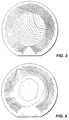
- Figs. 3-5 are maps of thickness uniformity across a wafer.
- FIG. 2 A plasma etch chamber in which the present preclean etch process can be carried out is shown in Fig. 2.
- a preclean chamber 100 is divided into two sections; a sputtering section 118 in which a wafer 117 to be cleaned is supported on a support electrode 119, and a plasma generation section 123.
- the chamber 100 has an exhaust channel 124 surrounding the electrode 119, which channel 124 is connected to a high vacuum pump 126 via a valve 127.
- An argon gas supply 129 feeds into the plasma generation section 123.
- a first RF generator 121 is connected to the substrate support electrode 119 via an RF match network 122. Suitably it provides RF energy of 13.56 MHz to the support electrode 119.
- This power source is turned on after a plasma has been ignited in the plasma generation section 123, as described hereinbelow, and serves to attract argon ions generated in the plasma. The argon ions strike the surface of the wafer 117 and sputter remove or etch the native oxide layer thereon.
- a second RF generator 138 is for example a 400 KHz power supply connected to a coil 136. This second RF generator 138 provides the power to form a plasma in the plasma generation section 123. This power supply is inductively coupled to the plasma. The role of plasma power is to increase the ion density in the plasma.
- the sputter etch rate is about 300 angstroms per minute. Thus it takes only about 10 seconds to sputter off the native oxide layer on a silicon wafer. However, in order to ensure that all of the oxide is removed, generally sputter etching is continued beyond that point, and a layer of silicon about 100 angstroms thick is also sputter etched. It is this silicon that heretofore has deposited on the walls of the etch chamber.
- the material deposited on the walls of the etch chamber is silicon oxide, which is a dielectric, it does not interfere with the supply of power to the chamber, and the cathode bias voltage remains constant.
- silicon oxide which is a dielectric
- the RF power coupling to the plasma is degraded and the DC bias voltage on the cathode drops, which decreases the sputter etch rate.
- the power dissipation in the silicon is evidenced by a rise in the wall temperature.
- the DC bias voltage on the cathode drops too low, the plasma is extinguished, particularly at the very low pressures desired for high sputter etch uniformity.
- oxygen in the plasma reacts with sputtered silicon from the substrate to form silicon oxide. Since silicon oxide deposits on the preclean etch chamber walls rather than silicon, and since silicon oxide does not dissipate the electrical power coupled to the chamber, the cathode bias voltage remains constant. Thus the second objective, to maintain the plasma even at very low pressures of 1 mT, is also achieved.
- the amount of oxygen added to the argon is not critical, although at least about 5% by volume of oxygen is required to achieve the objectives of the present invention. Since argon is a better sputter gas than oxygen, it is also preferred to have some argon present in the plasma precursor gas. Thus in general from about 5 to about 95% by volume of oxygen in argon is used to form the plasma precursor gas stream.
- silicon oxide will be formed which can theoretically re-deposit on the substrate surface.
- the temperature in the chamber is low during the preclean process, generally about 200-500°C, silicon and oxygen do not recombine to deposit silicon oxide on the surface, and the sputter etching takes precedence over silicon oxide deposition.
- the silicon substrate is a highly bonded, single crystal silicon substrate, which is not highly reactive, the silicon in the substrate does not readily react with oxygen ions in the plasma. Rather, the oxygen ions in the plasma react preferentially with the free silicon atoms or ions present in the plasma.
- the resultant silicon oxide is either evacuated through the chamber exhaust system, or deposited on nearby walls and fixtures, rather than on the wafer being sputter etched.
- a preclean chamber as in Fig. 2, the chamber was maintained at a pressure of at least 4 mT, while flowing argon gas into the chamber at a flow rate of about 60 sccm.
- a six inch silicon wafer was etched to remove about 30 angstroms ( ⁇ ) of silicon oxide and to perform an overetch of about 100 angstroms of silicon.
- the etch rate was 220 ⁇ /min.
- the etch depth varied from 160 ⁇ to 327 ⁇ across the wafer, with a high standard deviation of 19.79%, which is unacceptably high.
- the thickness variation map is shown in Fig. 3.
- Control A The procedure of Control A was repeated except that the gases fed to the chamber were a mixture of argon, 5 sccm, and oxygen, 3 sccm.
- the etch rate was 285 ⁇ /min and the thickness variation across the wafer was only 6.2%
- the thickness variation map is shown in Fig. 4.
- Example 2 The procedure of Example 1 was repeated except that 5 sccm of argon alone was fed to the chamber.
- the sputter etch rate was 614 ⁇ /min, but the plasma could not be sustained.
- the thickness variation map is shown in Fig. 5.
Landscapes
- Chemical & Material Sciences (AREA)
- Engineering & Computer Science (AREA)
- Metallurgy (AREA)
- Chemical Kinetics & Catalysis (AREA)
- Materials Engineering (AREA)
- Mechanical Engineering (AREA)
- Physics & Mathematics (AREA)
- Organic Chemistry (AREA)
- Plasma & Fusion (AREA)
- Optics & Photonics (AREA)
- General Chemical & Material Sciences (AREA)
- Drying Of Semiconductors (AREA)
- Cleaning Or Drying Semiconductors (AREA)
- ing And Chemical Polishing (AREA)
Applications Claiming Priority (2)
| Application Number | Priority Date | Filing Date | Title |
|---|---|---|---|
| US08/402,676 US5759360A (en) | 1995-03-13 | 1995-03-13 | Wafer clean sputtering process |
| US402676 | 1995-03-13 |
Publications (2)
| Publication Number | Publication Date |
|---|---|
| EP0732732A2 true EP0732732A2 (fr) | 1996-09-18 |
| EP0732732A3 EP0732732A3 (fr) | 1996-10-02 |
Family
ID=23592902
Family Applications (1)
| Application Number | Title | Priority Date | Filing Date |
|---|---|---|---|
| EP96103469A Withdrawn EP0732732A3 (fr) | 1995-03-13 | 1996-03-06 | Méthode d'enlèvement d'oxyde de silicium natif par pulvérisation |
Country Status (4)
| Country | Link |
|---|---|
| US (1) | US5759360A (fr) |
| EP (1) | EP0732732A3 (fr) |
| JP (1) | JPH08321491A (fr) |
| KR (1) | KR100386713B1 (fr) |
Cited By (6)
| Publication number | Priority date | Publication date | Assignee | Title |
|---|---|---|---|---|
| EP0926716A1 (fr) * | 1997-12-17 | 1999-06-30 | Sumitomo Metal Industries, Ltd. | Appareil et méthode de traitement par plasma |
| WO1999058739A1 (fr) * | 1998-05-12 | 1999-11-18 | Applied Materials, Inc. | Melange de gaz argon-oxygene permettant un pre-nettoyage dans un systeme de traitement sous vide |
| EP1186353A3 (fr) * | 2000-09-08 | 2002-04-10 | The Boc Group, Inc. | Traitement des bouteilles de gaz cylindriques |
| CN102218705A (zh) * | 2011-04-01 | 2011-10-19 | 苏州金宏气体股份有限公司 | 充装电子级超高纯气体的气瓶的处理方法 |
| EP2890835A1 (fr) * | 2012-08-31 | 2015-07-08 | Oerlikon Advanced Technologies AG | Procédé pour le dépôt d'une couche de nitrure d'aluminium |
| WO2020132175A1 (fr) * | 2018-12-21 | 2020-06-25 | Applied Materials, Inc. | Procédés de nettoyage d'une couche d'oxyde dans un empilement de films pour éliminer une formation d'arc pendant un traitement en aval |
Families Citing this family (22)
| Publication number | Priority date | Publication date | Assignee | Title |
|---|---|---|---|---|
| US6143144A (en) * | 1999-07-30 | 2000-11-07 | Tokyo Electronlimited | Method for etch rate enhancement by background oxygen control in a soft etch system |
| US6255179B1 (en) | 1999-08-04 | 2001-07-03 | International Business Machines Corporation | Plasma etch pre-silicide clean |
| KR20010062209A (ko) * | 1999-12-10 | 2001-07-07 | 히가시 데쓰로 | 고내식성 막이 내부에 형성된 챔버를 구비하는 처리 장치 |
| KR100421036B1 (ko) * | 2001-03-13 | 2004-03-03 | 삼성전자주식회사 | 웨이퍼 처리 장치 및 이를 이용한 웨이퍼 처리 방법 |
| US6798519B2 (en) * | 2002-09-30 | 2004-09-28 | Tokyo Electron Limited | Method and apparatus for an improved optical window deposition shield in a plasma processing system |
| US6837966B2 (en) * | 2002-09-30 | 2005-01-04 | Tokyo Electron Limeted | Method and apparatus for an improved baffle plate in a plasma processing system |
| US7204912B2 (en) * | 2002-09-30 | 2007-04-17 | Tokyo Electron Limited | Method and apparatus for an improved bellows shield in a plasma processing system |
| US7147749B2 (en) * | 2002-09-30 | 2006-12-12 | Tokyo Electron Limited | Method and apparatus for an improved upper electrode plate with deposition shield in a plasma processing system |
| US7166200B2 (en) * | 2002-09-30 | 2007-01-23 | Tokyo Electron Limited | Method and apparatus for an improved upper electrode plate in a plasma processing system |
| US7137353B2 (en) * | 2002-09-30 | 2006-11-21 | Tokyo Electron Limited | Method and apparatus for an improved deposition shield in a plasma processing system |
| US7166166B2 (en) | 2002-09-30 | 2007-01-23 | Tokyo Electron Limited | Method and apparatus for an improved baffle plate in a plasma processing system |
| TW200423195A (en) * | 2002-11-28 | 2004-11-01 | Tokyo Electron Ltd | Internal member of a plasma processing vessel |
| KR100918528B1 (ko) | 2003-03-31 | 2009-09-21 | 도쿄엘렉트론가부시키가이샤 | 처리부재 상에 인접한 코팅을 결합시키는 방법 |
| KR101016913B1 (ko) * | 2003-03-31 | 2011-02-22 | 도쿄엘렉트론가부시키가이샤 | 처리요소용 배리어층 및 그의 형성방법 |
| KR100560666B1 (ko) * | 2003-07-07 | 2006-03-16 | 삼성전자주식회사 | 반도체 소자 제조용 금속막 증착 시스템 및 그 운용 방법 |
| US7552521B2 (en) | 2004-12-08 | 2009-06-30 | Tokyo Electron Limited | Method and apparatus for improved baffle plate |
| US7601242B2 (en) | 2005-01-11 | 2009-10-13 | Tokyo Electron Limited | Plasma processing system and baffle assembly for use in plasma processing system |
| CN101330020B (zh) * | 2007-06-22 | 2010-05-19 | 中芯国际集成电路制造(上海)有限公司 | 一种晶圆缺陷的修复方法 |
| JP2016100343A (ja) * | 2014-11-18 | 2016-05-30 | 株式会社ディスコ | エッチング方法 |
| US10651233B2 (en) * | 2018-08-21 | 2020-05-12 | Northrop Grumman Systems Corporation | Method for forming superconducting structures |
| CN113539818B (zh) * | 2021-07-16 | 2024-05-03 | 长鑫存储技术有限公司 | 半导体结构的制造方法及半导体器件蚀刻设备 |
| US12211737B2 (en) * | 2021-08-27 | 2025-01-28 | Taiwan Semiconductor Manufacturing Company, Ltd. | Cleaning chamber for metal oxide removal |
Family Cites Families (14)
| Publication number | Priority date | Publication date | Assignee | Title |
|---|---|---|---|---|
| DE2547792C3 (de) * | 1974-10-25 | 1978-08-31 | Hitachi, Ltd., Tokio | Verfahren zur Herstellung eines Halbleiterbauelementes |
| US4298443A (en) * | 1979-08-09 | 1981-11-03 | Bell Telephone Laboratories, Incorporated | High capacity etching apparatus and method |
| US4326911A (en) * | 1980-01-29 | 1982-04-27 | Bell Telephone Laboratories, Incorporated | Reactive ion etching of III-V compounds including InP, GaAs-InP and GaAlAs |
| JPS56158873A (en) * | 1980-05-14 | 1981-12-07 | Hitachi Ltd | Dry etching method |
| FR2487808A1 (fr) * | 1980-08-01 | 1982-02-05 | Electricite De France | Procede et dispositif d'elimination du bore dans le silicium par fusion de zone sous plasma reactif |
| US4585517A (en) * | 1985-01-31 | 1986-04-29 | Motorola, Inc. | Reactive sputter cleaning of semiconductor wafer |
| JPS6221724A (ja) * | 1985-07-19 | 1987-01-30 | Furukawa Electric Co Ltd:The | ガラスパイプの内面研磨方法 |
| US4786352A (en) * | 1986-09-12 | 1988-11-22 | Benzing Technologies, Inc. | Apparatus for in-situ chamber cleaning |
| GB8629634D0 (en) * | 1986-12-11 | 1987-01-21 | Dobson C D | Reactive ion & sputter etching |
| US4951601A (en) * | 1986-12-19 | 1990-08-28 | Applied Materials, Inc. | Multi-chamber integrated process system |
| FR2616030A1 (fr) * | 1987-06-01 | 1988-12-02 | Commissariat Energie Atomique | Procede de gravure ou de depot par plasma et dispositif pour la mise en oeuvre du procede |
| US4786359A (en) * | 1987-06-24 | 1988-11-22 | Tegal Corporation | Xenon enhanced plasma etch |
| JP2758754B2 (ja) * | 1991-12-05 | 1998-05-28 | シャープ株式会社 | プラズマエッチング方法 |
| US5449432A (en) * | 1993-10-25 | 1995-09-12 | Applied Materials, Inc. | Method of treating a workpiece with a plasma and processing reactor having plasma igniter and inductive coupler for semiconductor fabrication |
-
1995
- 1995-03-13 US US08/402,676 patent/US5759360A/en not_active Expired - Fee Related
-
1996
- 1996-03-06 EP EP96103469A patent/EP0732732A3/fr not_active Withdrawn
- 1996-03-12 KR KR1019960006438A patent/KR100386713B1/ko not_active Expired - Fee Related
- 1996-03-13 JP JP8056439A patent/JPH08321491A/ja not_active Withdrawn
Cited By (6)
| Publication number | Priority date | Publication date | Assignee | Title |
|---|---|---|---|---|
| EP0926716A1 (fr) * | 1997-12-17 | 1999-06-30 | Sumitomo Metal Industries, Ltd. | Appareil et méthode de traitement par plasma |
| WO1999058739A1 (fr) * | 1998-05-12 | 1999-11-18 | Applied Materials, Inc. | Melange de gaz argon-oxygene permettant un pre-nettoyage dans un systeme de traitement sous vide |
| EP1186353A3 (fr) * | 2000-09-08 | 2002-04-10 | The Boc Group, Inc. | Traitement des bouteilles de gaz cylindriques |
| CN102218705A (zh) * | 2011-04-01 | 2011-10-19 | 苏州金宏气体股份有限公司 | 充装电子级超高纯气体的气瓶的处理方法 |
| EP2890835A1 (fr) * | 2012-08-31 | 2015-07-08 | Oerlikon Advanced Technologies AG | Procédé pour le dépôt d'une couche de nitrure d'aluminium |
| WO2020132175A1 (fr) * | 2018-12-21 | 2020-06-25 | Applied Materials, Inc. | Procédés de nettoyage d'une couche d'oxyde dans un empilement de films pour éliminer une formation d'arc pendant un traitement en aval |
Also Published As
| Publication number | Publication date |
|---|---|
| KR100386713B1 (ko) | 2003-08-21 |
| KR960035860A (ko) | 1996-10-28 |
| JPH08321491A (ja) | 1996-12-03 |
| US5759360A (en) | 1998-06-02 |
| EP0732732A3 (fr) | 1996-10-02 |
Similar Documents
| Publication | Publication Date | Title |
|---|---|---|
| US5759360A (en) | Wafer clean sputtering process | |
| US6110836A (en) | Reactive plasma etch cleaning of high aspect ratio openings | |
| US5454903A (en) | Plasma cleaning of a CVD or etch reactor using helium for plasma stabilization | |
| US5620526A (en) | In-situ cleaning of plasma treatment chamber | |
| US5382316A (en) | Process for simultaneous removal of photoresist and polysilicon/polycide etch residues from an integrated circuit structure | |
| JP2519383B2 (ja) | 窒化物上の酸化物層のエッチング方法 | |
| US6489248B2 (en) | Method and apparatus for etch passivating and etching a substrate | |
| JP3283477B2 (ja) | ドライエッチング方法および半導体装置の製造方法 | |
| KR101449081B1 (ko) | 기판 처리 방법 | |
| JP7522931B2 (ja) | 酸化物薄膜の製造方法 | |
| EP1827871B1 (fr) | Procedes destines a eliminer du silicium noir et du carbure de silicium noir de surfaces d'electrodes de silicium et de carbure de silicium pour des appareils de traitement au plasma | |
| US6156663A (en) | Method and apparatus for plasma processing | |
| KR20160088816A (ko) | 에칭 방법 | |
| US6573181B1 (en) | Method of forming contact structures using nitrogen trifluoride preclean etch process and a titanium chemical vapor deposition step | |
| EP4022670A1 (fr) | Films de carbone amorphe à densité, module et dureté élevés à basse pression | |
| KR20160088817A (ko) | 에칭 방법 | |
| JP4716566B2 (ja) | 基板上の銅酸化物を還元するプラズマ加工チャンバ、及び、その方法 | |
| US5880037A (en) | Oxide etch process using a mixture of a fluorine-substituted hydrocarbon and acetylene that provides high selectivity to nitride and is suitable for use on surfaces of uneven topography | |
| KR20160088819A (ko) | 에칭 방법 | |
| WO2023166987A1 (fr) | Masque dur, procédé de traitement de substrat et procédé d'élimination pour masque dur | |
| EP0791669B1 (fr) | Procédé de gravure de l'intérieur d'une chambre de réaction CVD | |
| CN1177204A (zh) | 刻蚀方法 | |
| EP0774772A1 (fr) | Procédé de gravure physique d'une surface électriquement conductrice en silicium | |
| JP2894304B2 (ja) | 半導体装置の製造方法 | |
| JP2002064067A (ja) | 化学気相成長を向上させるよう調整されたチャンバ |
Legal Events
| Date | Code | Title | Description |
|---|---|---|---|
| PUAI | Public reference made under article 153(3) epc to a published international application that has entered the european phase |
Free format text: ORIGINAL CODE: 0009012 |
|
| PUAL | Search report despatched |
Free format text: ORIGINAL CODE: 0009013 |
|
| AK | Designated contracting states |
Kind code of ref document: A2 Designated state(s): AT BE CH DE ES FR GB GR IE IT LI NL SE |
|
| AK | Designated contracting states |
Kind code of ref document: A3 Designated state(s): AT BE CH DE ES FR GB GR IE IT LI NL SE |
|
| 17P | Request for examination filed |
Effective date: 19970327 |
|
| 17Q | First examination report despatched |
Effective date: 20001012 |
|
| STAA | Information on the status of an ep patent application or granted ep patent |
Free format text: STATUS: THE APPLICATION IS DEEMED TO BE WITHDRAWN |
|
| 18D | Application deemed to be withdrawn |
Effective date: 20031001 |