EP0735156A2 - Procédé et appareil pour l'étamage partiel d'une bande - Google Patents
Procédé et appareil pour l'étamage partiel d'une bande Download PDFInfo
- Publication number
- EP0735156A2 EP0735156A2 EP96104657A EP96104657A EP0735156A2 EP 0735156 A2 EP0735156 A2 EP 0735156A2 EP 96104657 A EP96104657 A EP 96104657A EP 96104657 A EP96104657 A EP 96104657A EP 0735156 A2 EP0735156 A2 EP 0735156A2
- Authority
- EP
- European Patent Office
- Prior art keywords
- strips
- strip
- molten metal
- tape
- heating chamber
- Prior art date
- Legal status (The legal status is an assumption and is not a legal conclusion. Google has not performed a legal analysis and makes no representation as to the accuracy of the status listed.)
- Granted
Links
Images


Classifications
-
- C—CHEMISTRY; METALLURGY
- C23—COATING METALLIC MATERIAL; COATING MATERIAL WITH METALLIC MATERIAL; CHEMICAL SURFACE TREATMENT; DIFFUSION TREATMENT OF METALLIC MATERIAL; COATING BY VACUUM EVAPORATION, BY SPUTTERING, BY ION IMPLANTATION OR BY CHEMICAL VAPOUR DEPOSITION, IN GENERAL; INHIBITING CORROSION OF METALLIC MATERIAL OR INCRUSTATION IN GENERAL
- C23C—COATING METALLIC MATERIAL; COATING MATERIAL WITH METALLIC MATERIAL; SURFACE TREATMENT OF METALLIC MATERIAL BY DIFFUSION INTO THE SURFACE, BY CHEMICAL CONVERSION OR SUBSTITUTION; COATING BY VACUUM EVAPORATION, BY SPUTTERING, BY ION IMPLANTATION OR BY CHEMICAL VAPOUR DEPOSITION, IN GENERAL
- C23C2/00—Hot-dipping or immersion processes for applying the coating material in the molten state without affecting the shape; Apparatus therefor
- C23C2/04—Hot-dipping or immersion processes for applying the coating material in the molten state without affecting the shape; Apparatus therefor characterised by the coating material
- C23C2/08—Tin or alloys based thereon
-
- C—CHEMISTRY; METALLURGY
- C23—COATING METALLIC MATERIAL; COATING MATERIAL WITH METALLIC MATERIAL; CHEMICAL SURFACE TREATMENT; DIFFUSION TREATMENT OF METALLIC MATERIAL; COATING BY VACUUM EVAPORATION, BY SPUTTERING, BY ION IMPLANTATION OR BY CHEMICAL VAPOUR DEPOSITION, IN GENERAL; INHIBITING CORROSION OF METALLIC MATERIAL OR INCRUSTATION IN GENERAL
- C23C—COATING METALLIC MATERIAL; COATING MATERIAL WITH METALLIC MATERIAL; SURFACE TREATMENT OF METALLIC MATERIAL BY DIFFUSION INTO THE SURFACE, BY CHEMICAL CONVERSION OR SUBSTITUTION; COATING BY VACUUM EVAPORATION, BY SPUTTERING, BY ION IMPLANTATION OR BY CHEMICAL VAPOUR DEPOSITION, IN GENERAL
- C23C2/00—Hot-dipping or immersion processes for applying the coating material in the molten state without affecting the shape; Apparatus therefor
- C23C2/34—Hot-dipping or immersion processes for applying the coating material in the molten state without affecting the shape; Apparatus therefor characterised by the shape of the material to be treated
- C23C2/36—Elongated material
- C23C2/40—Plates; Strips
-
- Y—GENERAL TAGGING OF NEW TECHNOLOGICAL DEVELOPMENTS; GENERAL TAGGING OF CROSS-SECTIONAL TECHNOLOGIES SPANNING OVER SEVERAL SECTIONS OF THE IPC; TECHNICAL SUBJECTS COVERED BY FORMER USPC CROSS-REFERENCE ART COLLECTIONS [XRACs] AND DIGESTS
- Y10—TECHNICAL SUBJECTS COVERED BY FORMER USPC
- Y10T—TECHNICAL SUBJECTS COVERED BY FORMER US CLASSIFICATION
- Y10T428/00—Stock material or miscellaneous articles
- Y10T428/12—All metal or with adjacent metals
- Y10T428/12493—Composite; i.e., plural, adjacent, spatially distinct metal components [e.g., layers, joint, etc.]
- Y10T428/12708—Sn-base component
- Y10T428/12715—Next to Group IB metal-base component
-
- Y—GENERAL TAGGING OF NEW TECHNOLOGICAL DEVELOPMENTS; GENERAL TAGGING OF CROSS-SECTIONAL TECHNOLOGIES SPANNING OVER SEVERAL SECTIONS OF THE IPC; TECHNICAL SUBJECTS COVERED BY FORMER USPC CROSS-REFERENCE ART COLLECTIONS [XRACs] AND DIGESTS
- Y10—TECHNICAL SUBJECTS COVERED BY FORMER USPC
- Y10T—TECHNICAL SUBJECTS COVERED BY FORMER US CLASSIFICATION
- Y10T428/00—Stock material or miscellaneous articles
- Y10T428/12—All metal or with adjacent metals
- Y10T428/12493—Composite; i.e., plural, adjacent, spatially distinct metal components [e.g., layers, joint, etc.]
- Y10T428/12708—Sn-base component
- Y10T428/12722—Next to Group VIII metal-base component
-
- Y—GENERAL TAGGING OF NEW TECHNOLOGICAL DEVELOPMENTS; GENERAL TAGGING OF CROSS-SECTIONAL TECHNOLOGIES SPANNING OVER SEVERAL SECTIONS OF THE IPC; TECHNICAL SUBJECTS COVERED BY FORMER USPC CROSS-REFERENCE ART COLLECTIONS [XRACs] AND DIGESTS
- Y10—TECHNICAL SUBJECTS COVERED BY FORMER USPC
- Y10T—TECHNICAL SUBJECTS COVERED BY FORMER US CLASSIFICATION
- Y10T428/00—Stock material or miscellaneous articles
- Y10T428/12—All metal or with adjacent metals
- Y10T428/12993—Surface feature [e.g., rough, mirror]
-
- Y—GENERAL TAGGING OF NEW TECHNOLOGICAL DEVELOPMENTS; GENERAL TAGGING OF CROSS-SECTIONAL TECHNOLOGIES SPANNING OVER SEVERAL SECTIONS OF THE IPC; TECHNICAL SUBJECTS COVERED BY FORMER USPC CROSS-REFERENCE ART COLLECTIONS [XRACs] AND DIGESTS
- Y10—TECHNICAL SUBJECTS COVERED BY FORMER USPC
- Y10T—TECHNICAL SUBJECTS COVERED BY FORMER US CLASSIFICATION
- Y10T428/00—Stock material or miscellaneous articles
- Y10T428/24—Structurally defined web or sheet [e.g., overall dimension, etc.]
- Y10T428/24802—Discontinuous or differential coating, impregnation or bond [e.g., artwork, printing, retouched photograph, etc.]
- Y10T428/24917—Discontinuous or differential coating, impregnation or bond [e.g., artwork, printing, retouched photograph, etc.] including metal layer
Definitions
- the invention relates to a partially hot-dip tinned strip made of coatable material according to the preamble of claim 1.
- Partly tinned tapes on one or both sides can be produced, for example, by the process according to US Pat. No. 4,529,628.
- liquid metal is partially applied to a belt on one or both sides via a nozzle.
- the thickness of the coating is controlled by the belt speed and the nozzle output.
- the layer thickness is therefore identical across the entire range.
- the coating is continuous over the length of the belt. It is only possible to apply one coating material per strip side. If several coating materials or different properties are required on one strip side, several production steps in succession are necessary.
- this method does not offer the possibility of coating the strip edges, which is required with regard to solderability in the edge area or when making contact via the strip edge. This process is therefore not highly economical.
- the invention is therefore based on the object, in particular to expand the range of partially tinned strips in accordance with the needs of the electronics industry.
- the object is achieved in that the strip - seen in the longitudinal direction - is interrupted at regular and / or irregular intervals (A 1 , A 2 , A 3 ). Distances (A 1 , A 2 , A 3 %) in the range from 1 to 20 mm are preferred.
- the strips have different layer thicknesses (D1 / D2), or the strips consist of different coating materials.
- the advantages of thin Sn layers with, for example, low insertion and drawing forces can be shared the advantages of thick Sn layers combined with good solderability (especially for connectors).
- Harder coating materials e.g. in the contact zone with softer coating materials e.g. can be combined in the crimp or solder area.
- Copper, copper alloy, iron or iron alloy are preferred as the strip material; Pure tin, tin alloys or zinc are preferably available as coating materials.
- the invention further relates to methods and apparatus for producing the partially hot-dip tinned strip.
- the method assumes that the moving strip is provided with flux and heated and that molten metal is applied to the heated strip from at least one storage chamber via at least one opening and excess molten metal is stripped off.
- the method is characterized in that the supply of the molten metal from the opening is selectively opened and closed.
- different coating materials can also be used in one and the same strip.
- the storage chamber feeds at least two openings lying next to one another.
- the invention achieves structures in which the coating strips are notable for high adhesion.
- Partially tinned tapes are used in electronics and electrical engineering. They are used, for example, to manufacture connectors for the automotive industry, telecommunications and others. Some coated tapes are also used in the manufacture of semiconductor components such as QFPs (Quad Flat Package), SOTs (Small Outline Transistor), ICs (Integrated Circuit) and others here the combination of the bare strip surface with a well solderable tinned surface.
- QFPs Quad Flat Package
- SOTs Small Outline Transistor
- ICs Integrated Circuit
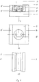
- the tape 1 according to Fig. 1 and 2 is each provided with four coating strips 2, 3, 4, 5. According to Figure 1, these are arranged approximately in the middle of the tape, according to Figure 2 on the tape edges. In both Fig.1 / 2, the strips 2, 3 on the top of the tape should have a layer thickness D1, the strips 4, 5 on the underside of the tape should have a layer thickness D2. Furthermore, it is indicated in FIG. 2 that the strips 2, 4 consist of a different coating material than the strips 3, 5. Only the two FIGS. 1/2 show the multiple possibilities of tinning the strip with different distances (A 1 , A 2 , A 3 ...) interrupted strips 2, 3, 4, 5.
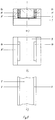
- the strip 1 running off a decoiler 6 passes through a flux feed 7 and for heating comes into a heating chamber 8, in which an insert 9 is integrated, in which a storage chamber 10 is arranged.
- the metal melt 11 located in the storage chamber 10 is thus kept at the same time at the temperature.
- the insert 9 rests resiliently on the belt 1.
- the metal melt 11 provided for coating can reach the strip 1 via an opening 12.
- Means for controlling the melt supply are indicated by paragraph 13.
- the layer thickness of the strip 2, 3, 4, 5 to be applied can be varied by the subsequent stripping 14 for the molten metal 11 and / or by the insert 9 being pressed more or less strongly onto the strip 1.
- the tinned strip 1 is finally rolled up on a reel 15.
- a storage chamber 10 feeds two openings 12 lying next to one another.
- the insert 9 has two storage chambers 10 opened laterally to the legs 8 'of the heating chamber 8, so that strips 2, 3, 4, 5 result on the edge strips.
- these storage chambers 10 are connected to grooves 16 in the heating chamber 8 which encompass the strip edges (means for controlling the supply of melt are not shown in more detail here).
- the heating chamber 8 which is essentially U-shaped in cross section, can consist, for example, of a base plate provided with heating cartridges, onto which a graphite plate and side legs 8 'are also screwed from graphite.
- Graphite can also be provided as the material for the insert 9.
- Tapes with the following dimensions can be tinned: thickness: 0.05 to 1.5 mm, width: 5 to 200 mm.
- Tinning temperature 50 to 400 ° C.
- Layer thicknesses of 0.2 to 25 ⁇ m can be achieved.
- the strips partially coated in this way have an intermetallic phase between the coating and the base material, which increases the adhesion of the coating, so that the coating does not flake off during bending processes even after heat treatments.
Landscapes
- Chemical & Material Sciences (AREA)
- Organic Chemistry (AREA)
- Engineering & Computer Science (AREA)
- Materials Engineering (AREA)
- Mechanical Engineering (AREA)
- Metallurgy (AREA)
- Chemical Kinetics & Catalysis (AREA)
- Coating With Molten Metal (AREA)
- Electroplating Methods And Accessories (AREA)
- Connection Of Batteries Or Terminals (AREA)
- Manufacturing Of Electrical Connectors (AREA)
- Bending Of Plates, Rods, And Pipes (AREA)
- Treatment Of Fiber Materials (AREA)
- Shaping Of Tube Ends By Bending Or Straightening (AREA)
- Vehicle Interior And Exterior Ornaments, Soundproofing, And Insulation (AREA)
Applications Claiming Priority (2)
| Application Number | Priority Date | Filing Date | Title |
|---|---|---|---|
| DE19511656 | 1995-03-30 | ||
| DE19511656A DE19511656C2 (de) | 1995-03-30 | 1995-03-30 | Partiell feuerverzinntes Band |
Publications (3)
| Publication Number | Publication Date |
|---|---|
| EP0735156A2 true EP0735156A2 (fr) | 1996-10-02 |
| EP0735156A3 EP0735156A3 (fr) | 1998-10-28 |
| EP0735156B1 EP0735156B1 (fr) | 2001-09-05 |
Family
ID=7758144
Family Applications (1)
| Application Number | Title | Priority Date | Filing Date |
|---|---|---|---|
| EP96104657A Expired - Lifetime EP0735156B1 (fr) | 1995-03-30 | 1996-03-23 | Procédé et appareil pour l'étamage partiel d'une bande |
Country Status (7)
| Country | Link |
|---|---|
| US (1) | US5712048A (fr) |
| EP (1) | EP0735156B1 (fr) |
| JP (1) | JP3954129B2 (fr) |
| AT (1) | ATE205262T1 (fr) |
| DE (2) | DE19511656C2 (fr) |
| DK (1) | DK0735156T3 (fr) |
| ES (1) | ES2161310T3 (fr) |
Cited By (1)
| Publication number | Priority date | Publication date | Assignee | Title |
|---|---|---|---|---|
| EP1857568A1 (fr) * | 2006-05-18 | 2007-11-21 | Wieland-Werke AG | Dispositif de revêtement et méthode pour fabrication d'une bande métallique partiellement revêtue sur une face |
Families Citing this family (4)
| Publication number | Priority date | Publication date | Assignee | Title |
|---|---|---|---|---|
| ITMI20042516A1 (it) * | 2004-12-27 | 2005-03-27 | Getters Spa | Processo per produrre mediante deposizione di lega bassofondente dispositivi portanti almeno un materiale attivo |
| DE102006033072B4 (de) * | 2006-07-14 | 2008-11-13 | Von Ardenne Anlagentechnik Gmbh | Verfahren und Vorrichtung zum Beschichten von Substraten durch Tauchen in eine Metallschmelze |
| EP1905857B1 (fr) | 2006-09-29 | 2013-08-14 | EZM Edelstahlzieherei Mark GmbH | Acier à haute résistance et utilisations d'un tel acier |
| DE102010054539A1 (de) * | 2010-12-15 | 2012-06-21 | OTB Oberflächentechnik in Berlin GmbH & Co. KG | Verfahren zur Herstellung eines Werkstücks aus Kupfer oder einer Kupferlegierung mit einer Beschichtung |
Family Cites Families (20)
| Publication number | Priority date | Publication date | Assignee | Title |
|---|---|---|---|---|
| DE278819C (fr) * | ||||
| US2274963A (en) * | 1938-08-10 | 1942-03-03 | Crucible Steel Company | Process for plating tin and tin alloys |
| US2394545A (en) * | 1942-08-28 | 1946-02-12 | Interchem Corp | Tin plate manufacture |
| JPS5130539B1 (fr) * | 1971-05-10 | 1976-09-01 | ||
| US3860780A (en) * | 1973-09-24 | 1975-01-14 | Dynaloc Corp | Method of making self-centering pulley using mig welding |
| JPS55145396A (en) * | 1979-04-27 | 1980-11-12 | Furukawa Circuit Foil | Copper foil for printed circuit and method of fabricating same |
| CH648601A5 (fr) * | 1979-07-31 | 1985-03-29 | Battelle Memorial Institute | Procede de revetement en continu d'un substrat metallique sur une partie au moins de sa surface par un autre metal et dispositif pour la mise en oeuvre de ce procede. |
| US4381342A (en) * | 1981-04-27 | 1983-04-26 | Eastman Kodak Company | Liquid jet method for coating photographic recording media |
| JPS5953666A (ja) * | 1982-09-22 | 1984-03-28 | Nippon Steel Corp | 部分めつき鋼帯 |
| JPS6115954A (ja) * | 1984-07-03 | 1986-01-24 | Sumitomo Electric Ind Ltd | 金属帯板用連続めつき方法とそれを実施するための装置 |
| JPS6115955A (ja) * | 1984-07-03 | 1986-01-24 | Sumitomo Electric Ind Ltd | 金属帯板用連続めつき装置 |
| JPS61235550A (ja) * | 1985-04-10 | 1986-10-20 | Nisshin Steel Co Ltd | メニスカスコ−テイング方法におけるめつき付着量の制御方法 |
| DE3536304A1 (de) * | 1985-10-11 | 1987-04-16 | Kaspar Eidenberg | Verfahren zum verzinnen von leiterplatten und vorrichtung zum durchfuehren dieses verfahrens |
| DE3539585A1 (de) * | 1985-10-11 | 1987-07-02 | Kaspar Eidenberg | Verfahren zum verloeten der anschluesse von bauteilen mit den leiterbahnen und loetaugen von leiterplatten und vorrichtung zum durchfuehren dieses verfahrens |
| DD278819A1 (de) * | 1988-12-27 | 1990-05-16 | Elektronische Bauelemente Dorf | Vorrichtung zum wahlweisen einseitigen schmelzfluessigen teilbeschichten von metallbaendern mit einer loetfaehigen schicht aus zinn oder zinn-blei-legierungen |
| WO1991006687A1 (fr) * | 1989-10-25 | 1991-05-16 | Nkk Corporation | Procede de placage en continu de plaques metalliques |
| DE4019090A1 (de) * | 1990-06-15 | 1991-12-19 | Battelle Institut E V | Verfahren zur beschichtung von substraten |
| FR2670505B1 (fr) * | 1990-12-17 | 1994-03-25 | Solems | Procede et appareil pour apporter un compose metallique fondu a un substrat. |
| US5429882A (en) * | 1993-04-05 | 1995-07-04 | The Louis Berkman Company | Building material coating |
| JP3264704B2 (ja) * | 1992-10-06 | 2002-03-11 | 松下電器産業株式会社 | 光学素子成形用金型およびその製造方法 |
-
1995
- 1995-03-30 DE DE19511656A patent/DE19511656C2/de not_active Expired - Fee Related
-
1996
- 1996-03-22 US US08/620,505 patent/US5712048A/en not_active Expired - Lifetime
- 1996-03-23 AT AT96104657T patent/ATE205262T1/de not_active IP Right Cessation
- 1996-03-23 ES ES96104657T patent/ES2161310T3/es not_active Expired - Lifetime
- 1996-03-23 DE DE59607603T patent/DE59607603D1/de not_active Expired - Lifetime
- 1996-03-23 EP EP96104657A patent/EP0735156B1/fr not_active Expired - Lifetime
- 1996-03-23 DK DK96104657T patent/DK0735156T3/da active
- 1996-03-26 JP JP09608996A patent/JP3954129B2/ja not_active Expired - Fee Related
Cited By (1)
| Publication number | Priority date | Publication date | Assignee | Title |
|---|---|---|---|---|
| EP1857568A1 (fr) * | 2006-05-18 | 2007-11-21 | Wieland-Werke AG | Dispositif de revêtement et méthode pour fabrication d'une bande métallique partiellement revêtue sur une face |
Also Published As
| Publication number | Publication date |
|---|---|
| ATE205262T1 (de) | 2001-09-15 |
| JPH08283924A (ja) | 1996-10-29 |
| DE59607603D1 (de) | 2001-10-11 |
| DE19511656C2 (de) | 1997-11-27 |
| DE19511656A1 (de) | 1996-10-02 |
| JP3954129B2 (ja) | 2007-08-08 |
| EP0735156B1 (fr) | 2001-09-05 |
| DK0735156T3 (da) | 2001-11-05 |
| ES2161310T3 (es) | 2001-12-01 |
| US5712048A (en) | 1998-01-27 |
| EP0735156A3 (fr) | 1998-10-28 |
Similar Documents
| Publication | Publication Date | Title |
|---|---|---|
| DE69404064T2 (de) | Flachkabelleiter, Verfahren und Vorrichtung zu dessen Herstellung | |
| DE60029264T2 (de) | Verfahren zur Herstellung von mehreren oberflächenmontierten Widerständen und oberflächenmontierter Widerstand | |
| EP0605800A1 (fr) | Résistances en matériel composite et procédé pour leur fabrication | |
| DE10045783A1 (de) | Verfahren zum Herstellen von Werkstücken, welche der Leitung von elektrischem Strom dienen und mit einem überwiegend metallischen Material beschichtet sind | |
| DE102015210458A1 (de) | Verfahren zum Verbinden eines ein unedles Metall aufweisenden Leiters mit einem Kupfer aufweisenden Anschlusselement mittels Verschweißen sowie eine dadurch hergestellte Anschlussanordnung | |
| DE69704678T2 (de) | Verfahren zum herstellen einer leiterplatteranordnung mit zinn/bleischicht | |
| DE1527541C3 (de) | Ausgangswerkstück zum Herstellen eines Verbundstoffstreifens für Lagermetallschalen | |
| EP0735156B1 (fr) | Procédé et appareil pour l'étamage partiel d'une bande | |
| DE2118375B2 (de) | Verfahren zum herstellen einer gedruckten schaltungskarte | |
| DE1521539C3 (de) | Verfahren zum Herstellen von weitgehend Korrosionsbeständigem draht- oder stangenförmigem Mehrschichtmaterial | |
| DE3613594C2 (fr) | ||
| DE3206262C2 (de) | Verfahren zur Herstellung von galvanisch selektiv mit Edelmetall beschichteten Bändern als Halbzeug für elektrische Kontakte | |
| WO1993018197A1 (fr) | Procede pour revetir de plusieurs couches un produit allonge | |
| DE4243141C2 (de) | Kaltspröde Kupfer-Phosphor-Lotlegierungen auf Kupferbändern | |
| DE2334534A1 (de) | Elektrischer stecker, insbesondere fuer gedruckte schaltungen, sowie verfahren zu seiner herstellung | |
| DE69328211T2 (de) | Einbau von elektronischen Komponenten auf Montageplatten mit Hilfe der Reflow-Technik | |
| AT516609B1 (de) | Elektrisch leitende Bauteile mit verbesserter Haftung und Verfahren zu deren Herstellung | |
| DE3047671C2 (de) | Verfahren zum kontinuierlichen schmelzflüssigen Überziehen von Metallteilen mit einer lötfähigen Schicht aus Zinn oder Zinn-Blei-Legierung und Vorrichtung zur Durchführung eines solchen Verfahrens | |
| DE2944613A1 (de) | Verfahren zum herstellen eines profildrahtes | |
| EP1815037B1 (fr) | Procede permettant de revetir d'un cote des bandes metalliques et utilisation de celles-ci | |
| DE3338347A1 (de) | Feuerverzinnen von anschlussbeinchen elektronischer bauelemente, die sich im verband eines traegerbandes befinden | |
| DE102005050221B4 (de) | Verfahren zum einseitigen Beschichten von Metallbändern und deren Verwendung | |
| DE102022112590A1 (de) | Verfahren zum Herstellen eines elektrischen Kontaktbauteils, insbesondere einer Stromschiene, sowie ein Kontaktbauteil | |
| EP0864666B1 (fr) | Procédé pour la fabrication d'une bande étamée | |
| CH666840A5 (de) | Verfahren, vorrichtung und anwendungen des verfahrens zur herstellung eines bandes, einer folie oder einer beschichtung aus metallischem oder metalloxydischem material. |
Legal Events
| Date | Code | Title | Description |
|---|---|---|---|
| PUAI | Public reference made under article 153(3) epc to a published international application that has entered the european phase |
Free format text: ORIGINAL CODE: 0009012 |
|
| 17P | Request for examination filed |
Effective date: 19960323 |
|
| AK | Designated contracting states |
Kind code of ref document: A2 Designated state(s): AT BE CH DE DK ES FR GB IT LI LU NL SE |
|
| PUAL | Search report despatched |
Free format text: ORIGINAL CODE: 0009013 |
|
| AK | Designated contracting states |
Kind code of ref document: A3 Designated state(s): AT BE CH DE DK ES FR GB IT LI LU NL SE |
|
| GRAG | Despatch of communication of intention to grant |
Free format text: ORIGINAL CODE: EPIDOS AGRA |
|
| GRAG | Despatch of communication of intention to grant |
Free format text: ORIGINAL CODE: EPIDOS AGRA |
|
| GRAH | Despatch of communication of intention to grant a patent |
Free format text: ORIGINAL CODE: EPIDOS IGRA |
|
| 17Q | First examination report despatched |
Effective date: 20010130 |
|
| GRAH | Despatch of communication of intention to grant a patent |
Free format text: ORIGINAL CODE: EPIDOS IGRA |
|
| GRAA | (expected) grant |
Free format text: ORIGINAL CODE: 0009210 |
|
| AK | Designated contracting states |
Kind code of ref document: B1 Designated state(s): AT BE CH DE DK ES FR GB IT LI LU NL SE |
|
| REF | Corresponds to: |
Ref document number: 205262 Country of ref document: AT Date of ref document: 20010915 Kind code of ref document: T |
|
| REG | Reference to a national code |
Ref country code: CH Ref legal event code: EP |
|
| REF | Corresponds to: |
Ref document number: 59607603 Country of ref document: DE Date of ref document: 20011011 |
|
| REG | Reference to a national code |
Ref country code: CH Ref legal event code: NV Representative=s name: A. BRAUN, BRAUN, HERITIER, ESCHMANN AG PATENTANWAE |
|
| REG | Reference to a national code |
Ref country code: DK Ref legal event code: T3 |
|
| REG | Reference to a national code |
Ref country code: ES Ref legal event code: FG2A Ref document number: 2161310 Country of ref document: ES Kind code of ref document: T3 |
|
| REG | Reference to a national code |
Ref country code: GB Ref legal event code: IF02 |
|
| GBT | Gb: translation of ep patent filed (gb section 77(6)(a)/1977) |
Effective date: 20011206 |
|
| ET | Fr: translation filed | ||
| PLBE | No opposition filed within time limit |
Free format text: ORIGINAL CODE: 0009261 |
|
| STAA | Information on the status of an ep patent application or granted ep patent |
Free format text: STATUS: NO OPPOSITION FILED WITHIN TIME LIMIT |
|
| 26N | No opposition filed | ||
| REG | Reference to a national code |
Ref country code: CH Ref legal event code: PFA Owner name: WIELAND-WERKE AG Free format text: WIELAND-WERKE AG#GRAF-ARCO-STRASSE 34#89079 ULM (DE) -TRANSFER TO- WIELAND-WERKE AG#GRAF-ARCO-STRASSE 34#89079 ULM (DE) |
|
| PGFP | Annual fee paid to national office [announced via postgrant information from national office to epo] |
Ref country code: SE Payment date: 20091218 Year of fee payment: 15 |
|
| PGFP | Annual fee paid to national office [announced via postgrant information from national office to epo] |
Ref country code: LU Payment date: 20100312 Year of fee payment: 15 Ref country code: DK Payment date: 20100312 Year of fee payment: 15 Ref country code: CH Payment date: 20100323 Year of fee payment: 15 |
|
| PGFP | Annual fee paid to national office [announced via postgrant information from national office to epo] |
Ref country code: IT Payment date: 20100320 Year of fee payment: 15 Ref country code: FR Payment date: 20100324 Year of fee payment: 15 |
|
| PGFP | Annual fee paid to national office [announced via postgrant information from national office to epo] |
Ref country code: GB Payment date: 20100317 Year of fee payment: 15 Ref country code: AT Payment date: 20100312 Year of fee payment: 15 |
|
| PGFP | Annual fee paid to national office [announced via postgrant information from national office to epo] |
Ref country code: ES Payment date: 20100408 Year of fee payment: 15 |
|
| PGFP | Annual fee paid to national office [announced via postgrant information from national office to epo] |
Ref country code: NL Payment date: 20100304 Year of fee payment: 15 Ref country code: DE Payment date: 20100331 Year of fee payment: 15 Ref country code: BE Payment date: 20100322 Year of fee payment: 15 |
|
| BERE | Be: lapsed |
Owner name: *WIELAND-WERKE A.G. Effective date: 20110331 |
|
| REG | Reference to a national code |
Ref country code: NL Ref legal event code: V1 Effective date: 20111001 |
|
| REG | Reference to a national code |
Ref country code: CH Ref legal event code: PL Ref country code: DK Ref legal event code: EBP |
|
| REG | Reference to a national code |
Ref country code: SE Ref legal event code: EUG |
|
| GBPC | Gb: european patent ceased through non-payment of renewal fee |
Effective date: 20110323 |
|
| PG25 | Lapsed in a contracting state [announced via postgrant information from national office to epo] |
Ref country code: AT Free format text: LAPSE BECAUSE OF NON-PAYMENT OF DUE FEES Effective date: 20110323 |
|
| REG | Reference to a national code |
Ref country code: FR Ref legal event code: ST Effective date: 20111130 |
|
| PG25 | Lapsed in a contracting state [announced via postgrant information from national office to epo] |
Ref country code: BE Free format text: LAPSE BECAUSE OF NON-PAYMENT OF DUE FEES Effective date: 20110331 |
|
| PG25 | Lapsed in a contracting state [announced via postgrant information from national office to epo] |
Ref country code: CH Free format text: LAPSE BECAUSE OF NON-PAYMENT OF DUE FEES Effective date: 20110331 Ref country code: FR Free format text: LAPSE BECAUSE OF NON-PAYMENT OF DUE FEES Effective date: 20110331 Ref country code: LI Free format text: LAPSE BECAUSE OF NON-PAYMENT OF DUE FEES Effective date: 20110331 Ref country code: NL Free format text: LAPSE BECAUSE OF NON-PAYMENT OF DUE FEES Effective date: 20111001 Ref country code: DE Free format text: LAPSE BECAUSE OF NON-PAYMENT OF DUE FEES Effective date: 20111001 |
|
| REG | Reference to a national code |
Ref country code: DE Ref legal event code: R119 Ref document number: 59607603 Country of ref document: DE Effective date: 20111001 |
|
| PG25 | Lapsed in a contracting state [announced via postgrant information from national office to epo] |
Ref country code: GB Free format text: LAPSE BECAUSE OF NON-PAYMENT OF DUE FEES Effective date: 20110323 Ref country code: IT Free format text: LAPSE BECAUSE OF NON-PAYMENT OF DUE FEES Effective date: 20110323 |
|
| REG | Reference to a national code |
Ref country code: ES Ref legal event code: FD2A Effective date: 20120423 |
|
| PG25 | Lapsed in a contracting state [announced via postgrant information from national office to epo] |
Ref country code: DK Free format text: LAPSE BECAUSE OF NON-PAYMENT OF DUE FEES Effective date: 20110331 |
|
| PG25 | Lapsed in a contracting state [announced via postgrant information from national office to epo] |
Ref country code: ES Free format text: LAPSE BECAUSE OF NON-PAYMENT OF DUE FEES Effective date: 20110324 |
|
| PG25 | Lapsed in a contracting state [announced via postgrant information from national office to epo] |
Ref country code: SE Free format text: LAPSE BECAUSE OF NON-PAYMENT OF DUE FEES Effective date: 20110324 |
|
| PG25 | Lapsed in a contracting state [announced via postgrant information from national office to epo] |
Ref country code: LU Free format text: LAPSE BECAUSE OF NON-PAYMENT OF DUE FEES Effective date: 20110323 |