EP0735576A2 - Fabrication de circuit intégré - Google Patents
Fabrication de circuit intégré Download PDFInfo
- Publication number
- EP0735576A2 EP0735576A2 EP96302136A EP96302136A EP0735576A2 EP 0735576 A2 EP0735576 A2 EP 0735576A2 EP 96302136 A EP96302136 A EP 96302136A EP 96302136 A EP96302136 A EP 96302136A EP 0735576 A2 EP0735576 A2 EP 0735576A2
- Authority
- EP
- European Patent Office
- Prior art keywords
- layer
- bonding pads
- fuses
- silicon nitride
- pads
- Prior art date
- Legal status (The legal status is an assumption and is not a legal conclusion. Google has not performed a legal analysis and makes no representation as to the accuracy of the status listed.)
- Withdrawn
Links
Images


Classifications
-
- H—ELECTRICITY
- H10—SEMICONDUCTOR DEVICES; ELECTRIC SOLID-STATE DEVICES NOT OTHERWISE PROVIDED FOR
- H10W—GENERIC PACKAGES, INTERCONNECTIONS, CONNECTORS OR OTHER CONSTRUCTIONAL DETAILS OF DEVICES COVERED BY CLASS H10
- H10W20/00—Interconnections in chips, wafers or substrates
- H10W20/01—Manufacture or treatment
- H10W20/031—Manufacture or treatment of conductive parts of the interconnections
- H10W20/064—Manufacture or treatment of conductive parts of the interconnections by modifying the conductivity of conductive parts, e.g. by alloying
-
- H—ELECTRICITY
- H10—SEMICONDUCTOR DEVICES; ELECTRIC SOLID-STATE DEVICES NOT OTHERWISE PROVIDED FOR
- H10W—GENERIC PACKAGES, INTERCONNECTIONS, CONNECTORS OR OTHER CONSTRUCTIONAL DETAILS OF DEVICES COVERED BY CLASS H10
- H10W72/00—Interconnections or connectors in packages
- H10W72/50—Bond wires
- H10W72/531—Shapes of wire connectors
- H10W72/536—Shapes of wire connectors the connected ends being ball-shaped
Definitions
- This invention relates to a process for fabricating an integrated circuit device and more particularly to a method for making a laser repair in the device.
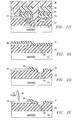
- FIG. 1(a) fuses 20 are fabricated in a polysilicon conductive layer that is surrounded by silicon dioxide 22. Bonding pads 24 are fabricated in a metal layer, which is covered by a layer of silicon dioxide 26 and a layer of silicon nitride 28, as in FIG. 1(b).
- a pix coating 30, e.g., a polymide resin, is laid over the silicon nitride patterned, and cured to provide access to the pads and fuses, as in FIGS. 1(c) and (d).
- the pix coating, the silicon nitride, and the silicon dioxide are etched away from the pads for direct access for electrical testing, as shown in FIG. 1(e) and 1(f).
- the pix coating, the silicon nitride, and a part of the silicon dioxide are etched away from above the fuses for laser trimming, as shown in FIG. 1(g).
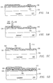
- test fuses 40 are fabricated in a polysilicon conductive layer surrounded by silicon dioxide 42 similar to the first method, as shown in FIG. 2(a). Thereafter a cap oxide 44, e.g., silicon dioxide, is deposited over the metallic layer 46 and silicon dioxide 42. The cap oxide is sintered and the surface of the device is patterned to nearly expose the fuses 40 of the device, as shown in FIG. 2(b). The cap oxide also is etched away from over the pads 46. The silicon dioxide is etched down nearly to the level of the fuses.
- electrical tests are performed through probes 48 contacting with the exposed pads, and a laser beam 50 is used for trimming fuses, as shown in FIG. 2(d).
- a silicon nitride layer 52 is deposited over the top of the device and into the fuse cavity, as shown in FIG. 2(e).
- a pix coating 54 is laid over the silicon nitride 52 and patterned to provide access to the pads, as shown in FIG 2(f).
- the pix material and the silicon nitride are etched to expose the pads for use in a system, as--shown in FIGS. 2(g) and 2(h).
- Bonding wires 56 are connected to the bonding pads 46, and a molding compound 58 is added to encapsulate the device.
- a disadvantage to this method is that a second costly masking sequence is added into the sequence of processing steps.
- An advantage in this process is that the silicon nitride protects the non-trimmed fuses from deleterious effects which can occur if those fuses are left unprotected from the ambient atmosphere.
- a method for fabricating a semiconductor device including the steps of: forming fuses in a first metallic layer; covering the first metallic layer with an insulator layer; forming conductive pads in a second metallic layer; depositing a layer of cap oxide over the pads and the insulator layer; etching back the layer of cap oxide until the top surfaces of the conductive pads and of the insulator layer over the fuses are exposed and sidewall oxides remain on the conducting pads; performing electrical tests; trimming at least a part of the fuses with a laser beam; depositing a silicon nitride layer; depositing a mask coating over the silicon nitride layer; patterning the mask coating for exposing the conductive pads; and etching the pix coating and the silicon nitride layer to expose the conductive pads.
- An advantage of this method is that it is relatively low cost because only one masking sequence is used in the sequence of steps. Risk of deleterious effects is low because the fuses are covered by the silicon nitride after the laser trimming operation.
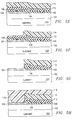
- FIGS. 3(a) through 3(i) there is shown a new sequence of steps in the process of fabricating an integrated circuit semiconductor device. This sequence of steps relates to the testing of circuits within the device, and to the switching good redundant circuits in replacement of defective regular circuits.
- FIG. 3(a) there is shown a fuse 60 fabricated in a metallic layer surrounded by a dielectric 62, such as silicon dioxide 62.
- the dielectric 62 is laid over a silicon substrate 63.
- a conductive metallic pad 64 formed for making interconnections between circuits built within the device (but not shown) and other external circuits.
- a layer of dielectric cap oxide 66 which may be silicon dioxide, is laid over the pad 64.
- a sinter operation is performed at this stage of device fabrication.
- the device is shown following an overall cap oxide etch back which removes the cap oxide 66 down to the top surface of the conductive pad 64 and to the top surface insulator 62.
- a sidewall insulator 67 is left on the conductive pad 64.
- the silicon dioxide cap oxide mixture of CHF 3 , CF 4 and Ar may be used in a ratio of approximately 20/20/1000.
- FIG. 3(c) shows an electrical probe from a testing apparatus making contact with the conductive pad 64 for making quality control tests. Some circuit defects may be uncovered as a result of the tests. Some of those defects can be removed from active operation of the device and can be replaced by other good redundant circuits by opening one or more fuses in the device.
- FIG. 3(d) shows a laser beam 70 which is used for blowing a fuse leaving a blow fuse cavity where the fuse 60 had been located. After all of the fuses are blown, as desired, an insulative layer 72, such as silicon nitride Si 3 N 4 is over the entire device and filling in the blown fuse cavities, as shown in FIG. 3(e).
- an insulative layer 72 such as silicon nitride Si 3 N 4 is over the entire device and filling in the blown fuse cavities, as shown in FIG. 3(e).
- FIG. 3(f) there is shown a masking material 74 laid over the top of the device. This may be a photoresist that can be patterned and cured for exposing the conductive pads 64, as shown in FIG. 3(g).
- the patterned mask is used for etching back the insulative layer of silicon nitride to fully expose the conductive pads 64.
- a gas mixture of CF 4 , oxygen, and nitrogen in a ratio of 120/30/20 may be used for the etching of the silicon nitride.
- bonding wires such as the wire 76, are bonded to the conductive pad 64 for interconnecting with external circuits, which are not shown.
- a molding compound 78 is applied thereafter to protect the device from harmful effect of the atmosphere and other hazards.
- the etching is accomplished without the need for a mask.
- the etching is applied universally over the entire device. This saves an otherwise expense sequence of steps for forming and removing masking material.
- the bonding pads are exposed for testing while the top level of metallic wiring retains sidewall oxide to prevent electrical shorting and hillock growth.
- the silicon nitride film is applied to improve reliability by preventing deleterious effects caused by ambient atmospheric conditions. Additional area consuming moisture barrier structures are not used.
- a lower cost sequence of process steps are presented for making electrical tests, for trimming desired fuses, and for providing good hermetic sealing.
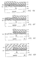
- FIGS. 4(a) through 4(h) there is presented another low cost sequence of steps for testing internal circuits of a semiconductor device and replacing defective ones of them with good redundant circuits.
- the device is shown including a fuse 80 surrounded by a dielectric 82 over a semiconductor substrate 83.
- a conductive pad 84 is laid on top of the dielectric 84.
- the fuse 80 and conductive pad 84 represent many of each.
- a test probe is connected to the conductive pad 84 for performing electrical tests, as shown in FIG. 4(b).
- defective circuits are replaced by good redundant circuits by laser beam 88 trimming of the fuses.
- a fuse cavity is opened where fuses are blown.
- a dielectric layer 90 of silicon nitride Si 3 N 4 is laid universally over the top of the device to cover the conductive pads 84 and to fill the fuse cavities.
- a masking material 92 such as a photoresist, is laid over the entire device, as shown in FIG. 4(e).
- the masking material 92 is patterned for exposing the conductive pad and is cured. Then the silicon nitride layer is etched back from the top of the conductive pads 84 to expose those pads.
- the previously mentioned mixture of CF 4 , oxygen, and nitrogen can be used as the etchant. Bonding wires, such as the wire 94, are connected to the conductive pads 84 and a molding compound 96 is applied.
- This sequence of processing steps has the further advantage of eliminating the steps of applying the cap oxide and etching back, as included in the sequence of FIG. 3.
- FIGS. 5(a) through 5(h) there is shown another variation of the new sequence of steps for testing for defective circuits and for replacing defective ones with good ones.
- the device is shown including a metallicfuse 100 fabricated in the same metal level as the conductive pad 104 on the top surface of an cap oxide insulator layer 102, which may be silicon dioxide. They are fabricated on top of a substrate 103. An insulative layer of silicon dioxide 106 covers the fuses 100, the conductive pads 104, and the silicon dioxide 102.
- a test probe 108 is mechanically pushed through the cap oxide 106 to contact the conductive pad 104 for testing internal circuits, not shown. Defective circuits are replaced by good redundant circuits by laser beam 110 trimming, as shown in FIG. 5(c). Cavities are left in the cap oxide 106 where the test probe was inserted and where any fuse was blown.
- a layer of silicon nitride 112 is laid over the entire device to cover the conductive pads 104 and the cap oxide 106 and to fill cavities in the cap oxide. Thereafter a masking material 114 is deposited overall, as shown in FIG. 5(e), is patterned, and is cured for exposing the conductive pads 104, as shown in FIG. 5(f).
- the silicon nitride layer 112 and the cap oxide are etched back to expose the surface of the conductive pads 104. Appropriate etchants are used. Finally bonding wires 116 are connected to the conductive pads 104 and a molding compound 118 is applied to protect the device.
- the cost of the testing and redundancy replacement steps is reduced because the conductive pads are exposed for testing without a sequence of masking steps, and additional moisture barrier structures are avoided.
- FIGS. 6(a) through 6(h) there is shown a further variation for testing and for replacing defective circuits.
- the sequence of steps is similar to the sequence of steps shown in FIGS. 5(a) through 5(h) so identical reference numerals are used to represent the same elements.
- the sequence of steps is identical except for the step shown in FIG. 6(b).
- a chemical etch is used to aid penetration through the cap oxide.
- the probe is first partially immersed in an etchant 120 and then is pressed through the cap oxide 106 to contact the conductive pad 104.
Landscapes
- Design And Manufacture Of Integrated Circuits (AREA)
- Drying Of Semiconductors (AREA)
- Semiconductor Memories (AREA)
- Semiconductor Integrated Circuits (AREA)
Applications Claiming Priority (2)
| Application Number | Priority Date | Filing Date | Title |
|---|---|---|---|
| US08/413,291 US5641701A (en) | 1995-03-30 | 1995-03-30 | Method for fabricating a semiconductor device with laser programable fuses |
| US413291 | 1995-03-30 |
Publications (2)
| Publication Number | Publication Date |
|---|---|
| EP0735576A2 true EP0735576A2 (fr) | 1996-10-02 |
| EP0735576A3 EP0735576A3 (fr) | 1999-01-13 |
Family
ID=23636671
Family Applications (1)
| Application Number | Title | Priority Date | Filing Date |
|---|---|---|---|
| EP96302136A Withdrawn EP0735576A3 (fr) | 1995-03-30 | 1996-03-27 | Fabrication de circuit intégré |
Country Status (5)
| Country | Link |
|---|---|
| US (1) | US5641701A (fr) |
| EP (1) | EP0735576A3 (fr) |
| JP (1) | JPH08274180A (fr) |
| KR (1) | KR100384964B1 (fr) |
| TW (1) | TW319907B (fr) |
Cited By (1)
| Publication number | Priority date | Publication date | Assignee | Title |
|---|---|---|---|---|
| DE10123686C1 (de) * | 2001-05-15 | 2003-03-20 | Infineon Technologies Ag | Verfahren zur Herstellung eines elektronischen Bauelements, insbesondere eines Speicherchips und dadurch hergestelltes elektronische Bauelement |
Families Citing this family (10)
| Publication number | Priority date | Publication date | Assignee | Title |
|---|---|---|---|---|
| JPH10163867A (ja) * | 1996-11-29 | 1998-06-19 | Ricoh Co Ltd | クロックジェネレータおよび製造方法 |
| KR100241061B1 (ko) * | 1997-07-26 | 2000-02-01 | 윤종용 | 반도체장치의퓨즈제조방법및퓨즈를가진반도체장치 |
| KR100502401B1 (ko) * | 1997-09-03 | 2005-10-06 | 삼성전자주식회사 | 광학간섭계의조정용공구 |
| US6017824A (en) * | 1998-11-16 | 2000-01-25 | Taiwan Semiconductor Manufacturing Company | Passivation etching procedure, using a polysilicon stop layer, for repairing embedded DRAM cells |
| US6177297B1 (en) * | 1999-01-11 | 2001-01-23 | United Microelectronics Corp. | Method of forming metallic fuse demanding lower laser power for circuit repair |
| US6210995B1 (en) | 1999-09-09 | 2001-04-03 | International Business Machines Corporation | Method for manufacturing fusible links in a semiconductor device |
| US6667195B2 (en) * | 2001-08-06 | 2003-12-23 | United Microelectronics Corp. | Laser repair operation |
| KR100449029B1 (ko) * | 2002-04-04 | 2004-09-16 | 삼성전자주식회사 | 패드영역에 퓨즈박스를 구비한 반도체 장치 및 그의제조방법 |
| TWI243455B (en) | 2002-11-27 | 2005-11-11 | Siliconware Precision Industries Co Ltd | Ball grid array semiconductor package |
| CN113013090B (zh) * | 2021-02-07 | 2022-06-24 | 长鑫存储技术有限公司 | 半导体结构的熔断填充方法及半导体结构 |
Family Cites Families (7)
| Publication number | Priority date | Publication date | Assignee | Title |
|---|---|---|---|---|
| JPS59214239A (ja) * | 1983-05-16 | 1984-12-04 | Fujitsu Ltd | 半導体装置の製造方法 |
| JPS60176250A (ja) * | 1984-02-23 | 1985-09-10 | Toshiba Corp | 半導体装置の製造方法 |
| US5252844A (en) * | 1988-11-17 | 1993-10-12 | Mitsubishi Denki Kabushiki Kaisha | Semiconductor device having a redundant circuit and method of manufacturing thereof |
| US5025300A (en) * | 1989-06-30 | 1991-06-18 | At&T Bell Laboratories | Integrated circuits having improved fusible links |
| US5241212A (en) * | 1990-05-01 | 1993-08-31 | Mitsubishi Denki Kabushiki Kaisha | Semiconductor device having a redundant circuit portion and a manufacturing method of the same |
| US5326709A (en) * | 1991-12-19 | 1994-07-05 | Samsung Electronics Co., Ltd. | Wafer testing process of a semiconductor device comprising a redundancy circuit |
| JPH0737988A (ja) * | 1993-07-20 | 1995-02-07 | Hitachi Ltd | 半導体集積回路装置の製造方法 |
-
1995
- 1995-03-30 US US08/413,291 patent/US5641701A/en not_active Expired - Lifetime
-
1996
- 1996-03-27 EP EP96302136A patent/EP0735576A3/fr not_active Withdrawn
- 1996-03-29 JP JP8077123A patent/JPH08274180A/ja active Pending
- 1996-03-29 KR KR1019960009130A patent/KR100384964B1/ko not_active Expired - Lifetime
- 1996-04-25 TW TW085104920A patent/TW319907B/zh not_active IP Right Cessation
Cited By (2)
| Publication number | Priority date | Publication date | Assignee | Title |
|---|---|---|---|---|
| DE10123686C1 (de) * | 2001-05-15 | 2003-03-20 | Infineon Technologies Ag | Verfahren zur Herstellung eines elektronischen Bauelements, insbesondere eines Speicherchips und dadurch hergestelltes elektronische Bauelement |
| US7338843B2 (en) | 2001-05-15 | 2008-03-04 | Infineon Technologies Ag | Method for producing an electronic component, especially a memory chip |
Also Published As
| Publication number | Publication date |
|---|---|
| US5641701A (en) | 1997-06-24 |
| JPH08274180A (ja) | 1996-10-18 |
| KR100384964B1 (ko) | 2003-08-21 |
| TW319907B (fr) | 1997-11-11 |
| EP0735576A3 (fr) | 1999-01-13 |
Similar Documents
| Publication | Publication Date | Title |
|---|---|---|
| US8901733B2 (en) | Reliable metal bumps on top of I/O pads after removal of test probe marks | |
| US4628590A (en) | Method of manufacture of a semiconductor device | |
| EP0128675B1 (fr) | Procédé de fabrication d'un circuit intégré à métallisation multicouche avec un fusible et une ouverture pour le fusible | |
| US5023205A (en) | Method of fabricating hybrid circuit structures | |
| JP3881393B2 (ja) | 半導体デバイスの製造方法 | |
| KR100447968B1 (ko) | 웨이퍼 레벨 패키지의 제조방법 | |
| US5641701A (en) | Method for fabricating a semiconductor device with laser programable fuses | |
| JPH1084042A (ja) | 半導体装置およびその製造方法並びに半導体中にピッチが密接したポリシリコン・ヒューズを形成する方法 | |
| US6458630B1 (en) | Antifuse for use with low k dielectric foam insulators | |
| US5474651A (en) | Method for filling via holes in a semiconductor layer structure | |
| US6022762A (en) | Process for forming a morphological edge structure to seal integrated electronic devices | |
| US4882293A (en) | Method of making an electrically programmable integrated circuit containing meltable contact bridges | |
| US5789796A (en) | Programmable anti-fuse device and method for manufacturing the same | |
| US7785935B2 (en) | Manufacturing method for forming an integrated circuit device and corresponding integrated circuit device | |
| US6248657B1 (en) | Semiconductor device and method for manufacturing the same | |
| JPH09139431A (ja) | 半導体装置とその製造方法 | |
| EP0583119A1 (fr) | Structure de contact programmable et sa méthode de formation | |
| US5610100A (en) | Method for concurrently forming holes for interconnection between different conductive layers and a substrate element or circuit element close to the substrate surface | |
| US7763951B2 (en) | Fuse structure for maintaining passivation integrity | |
| KR940007290B1 (ko) | 와이어 본딩 패드 형성방법 | |
| KR0177405B1 (ko) | 반도체 장치의 안티퓨즈 및 그 제조방법 | |
| KR20020001019A (ko) | 퓨즈를 갖는 반도체 장치의 제조 방법 | |
| KR0151224B1 (ko) | 반도체 소자의 전도층간 연결방법 | |
| CN121376905A (zh) | 一种mems器件及其封装方法 | |
| KR100216730B1 (ko) | 반도체 금속막 식각공정 |
Legal Events
| Date | Code | Title | Description |
|---|---|---|---|
| PUAI | Public reference made under article 153(3) epc to a published international application that has entered the european phase |
Free format text: ORIGINAL CODE: 0009012 |
|
| AK | Designated contracting states |
Kind code of ref document: A2 Designated state(s): DE FR GB IT NL |
|
| PUAL | Search report despatched |
Free format text: ORIGINAL CODE: 0009013 |
|
| RHK1 | Main classification (correction) |
Ipc: H01L 21/268 |
|
| AK | Designated contracting states |
Kind code of ref document: A3 Designated state(s): DE FR GB IT NL |
|
| 17P | Request for examination filed |
Effective date: 19990709 |
|
| 17Q | First examination report despatched |
Effective date: 20040205 |
|
| STAA | Information on the status of an ep patent application or granted ep patent |
Free format text: STATUS: THE APPLICATION IS DEEMED TO BE WITHDRAWN |
|
| 18D | Application deemed to be withdrawn |
Effective date: 20040817 |