EP0735582A1 - Packung zur Montage eines IC-Chips - Google Patents
Packung zur Montage eines IC-Chips Download PDFInfo
- Publication number
- EP0735582A1 EP0735582A1 EP96410031A EP96410031A EP0735582A1 EP 0735582 A1 EP0735582 A1 EP 0735582A1 EP 96410031 A EP96410031 A EP 96410031A EP 96410031 A EP96410031 A EP 96410031A EP 0735582 A1 EP0735582 A1 EP 0735582A1
- Authority
- EP
- European Patent Office
- Prior art keywords
- platform
- chip
- grid
- connection
- pins
- Prior art date
- Legal status (The legal status is an assumption and is not a legal conclusion. Google has not performed a legal analysis and makes no representation as to the accuracy of the status listed.)
- Granted
Links
Images


Classifications
-
- H—ELECTRICITY
- H10—SEMICONDUCTOR DEVICES; ELECTRIC SOLID-STATE DEVICES NOT OTHERWISE PROVIDED FOR
- H10W—GENERIC PACKAGES, INTERCONNECTIONS, CONNECTORS OR OTHER CONSTRUCTIONAL DETAILS OF DEVICES COVERED BY CLASS H10
- H10W70/00—Package substrates; Interposers; Redistribution layers [RDL]
- H10W70/40—Leadframes
- H10W70/464—Additional interconnections in combination with leadframes
- H10W70/468—Circuit boards
-
- H—ELECTRICITY
- H10—SEMICONDUCTOR DEVICES; ELECTRIC SOLID-STATE DEVICES NOT OTHERWISE PROVIDED FOR
- H10W—GENERIC PACKAGES, INTERCONNECTIONS, CONNECTORS OR OTHER CONSTRUCTIONAL DETAILS OF DEVICES COVERED BY CLASS H10
- H10W70/00—Package substrates; Interposers; Redistribution layers [RDL]
- H10W70/40—Leadframes
- H10W70/421—Shapes or dispositions
-
- H—ELECTRICITY
- H10—SEMICONDUCTOR DEVICES; ELECTRIC SOLID-STATE DEVICES NOT OTHERWISE PROVIDED FOR
- H10W—GENERIC PACKAGES, INTERCONNECTIONS, CONNECTORS OR OTHER CONSTRUCTIONAL DETAILS OF DEVICES COVERED BY CLASS H10
- H10W72/00—Interconnections or connectors in packages
- H10W72/50—Bond wires
- H10W72/541—Dispositions of bond wires
- H10W72/5449—Dispositions of bond wires not being orthogonal to a side surface of the chip, e.g. fan-out arrangements
-
- H—ELECTRICITY
- H10—SEMICONDUCTOR DEVICES; ELECTRIC SOLID-STATE DEVICES NOT OTHERWISE PROVIDED FOR
- H10W—GENERIC PACKAGES, INTERCONNECTIONS, CONNECTORS OR OTHER CONSTRUCTIONAL DETAILS OF DEVICES COVERED BY CLASS H10
- H10W72/00—Interconnections or connectors in packages
- H10W72/50—Bond wires
- H10W72/551—Materials of bond wires
- H10W72/552—Materials of bond wires comprising metals or metalloids, e.g. silver
- H10W72/5522—Materials of bond wires comprising metals or metalloids, e.g. silver comprising gold [Au]
-
- H—ELECTRICITY
- H10—SEMICONDUCTOR DEVICES; ELECTRIC SOLID-STATE DEVICES NOT OTHERWISE PROVIDED FOR
- H10W—GENERIC PACKAGES, INTERCONNECTIONS, CONNECTORS OR OTHER CONSTRUCTIONAL DETAILS OF DEVICES COVERED BY CLASS H10
- H10W74/00—Encapsulations, e.g. protective coatings
-
- H—ELECTRICITY
- H10—SEMICONDUCTOR DEVICES; ELECTRIC SOLID-STATE DEVICES NOT OTHERWISE PROVIDED FOR
- H10W—GENERIC PACKAGES, INTERCONNECTIONS, CONNECTORS OR OTHER CONSTRUCTIONAL DETAILS OF DEVICES COVERED BY CLASS H10
- H10W90/00—Package configurations
- H10W90/701—Package configurations characterised by the relative positions of pads or connectors relative to package parts
- H10W90/751—Package configurations characterised by the relative positions of pads or connectors relative to package parts of bond wires
- H10W90/756—Package configurations characterised by the relative positions of pads or connectors relative to package parts of bond wires between a chip and a stacked lead frame, conducting package substrate or heat sink
-
- Y—GENERAL TAGGING OF NEW TECHNOLOGICAL DEVELOPMENTS; GENERAL TAGGING OF CROSS-SECTIONAL TECHNOLOGIES SPANNING OVER SEVERAL SECTIONS OF THE IPC; TECHNICAL SUBJECTS COVERED BY FORMER USPC CROSS-REFERENCE ART COLLECTIONS [XRACs] AND DIGESTS
- Y10—TECHNICAL SUBJECTS COVERED BY FORMER USPC
- Y10T—TECHNICAL SUBJECTS COVERED BY FORMER US CLASSIFICATION
- Y10T29/00—Metal working
- Y10T29/49—Method of mechanical manufacture
- Y10T29/49002—Electrical device making
- Y10T29/49117—Conductor or circuit manufacturing
- Y10T29/49121—Beam lead frame or beam lead device
Definitions
- the present invention relates to the production of an integrated circuit package. It applies more particularly to the production of a box for mounting an integrated circuit chip from a connection grid defining electrical connection pins of the studs of the chip towards the outside of the box.
- FIG. 1 partially shows, in top view, the conventional structure of a grid 1 intended to allow the electrical connections of a chip to the outside of a housing.
- FIG. 2 represents a sectional view of a mounting box for an integrated circuit chip 2 using a grid 1 as shown in FIG. 1.
- the section plane of FIG. 2 corresponds to the line AA 'in figure 1.
- the grid 1 consists of a frame 1 ′ surrounding a central platform 3 intended to support the chip 2.
- Connection pins 4 extend from the frame towards the platform 3 without reaching the latter.
- Various parts of the grid interconnect the pins 4 to ensure a certain rigidity during assembly.
- the platform 3 is held by straps 4 'extending from the corners of the platform to the frame 1'.
- On the pins 4 are welded ends of conductive wires 5 connecting each pin 4 to one of the studs that includes the chip 2 on its upper face.
- the assembly is then encapsulated by means of an insulating resin 6 which defines the envelope of the housing. After encapsulation, the frame 1 ′ and the short circuits between the pins 4 are removed by cutting out.
- the conducting wires 5 are generally gold wires.
- the resin 6 is generally an epoxy resin and the grid 1 is generally made of copper or iron-nickel.
- the grid 1 is generally produced by mechanical punching of a copper sheet. It can sometimes be carried out by chemical cutting (photolithography) but the use of this technique for mass production is avoided because such a process is slow and more expensive.
- a disadvantage of mechanical punching is that it requires a specific punching tool for each type of chip 2 because the dimensions of the platforms 3 must be adapted to the dimensions of the chips 2 to limit the length of the wires 5. If the punching is rapid and therefore provides good productivity, the production of each punch and of the tool matrix is particularly expensive.
- a heat sink is attached below the platform 3 either by gluing or by soldering.
- a drawback which one meets in this type of applications is the stacking of thermal interfaces between the chip and the dissipator which harms the dissipation of energy.
- the chip 2 must be electrically isolated from the dissipator or from the platform. An insulator is then placed under the chip, which increases the number of thermal interfaces. In addition, the insulation and glue required for its fixing are generally organic and accumulate moisture. An excess of humidity risks cracking the resin 6 during its polymerization in an oven or even later when the housing is subjected to high temperatures (wave soldering or soldering in an oven of surface-mounted components).
- the invention aims to provide a housing comprising a heat sink which eliminates the thermal interfaces between the chip and the housing while reducing the humidity accumulated in the housing.
- connection grid uses a method of producing a connection grid, which is described in US Patent No. 5,256,598.
- a single connection grid is provided for mounting chips of different sizes, this grid comprising connection pins extending towards a central area of as small a size as possible, close to that of the smallest chip to be mounted.
- the connection pins are cut around the central zone to the dimensions of the chip to be mounted, and a platform is fixed on the grid.
- the platform is made of an anodized metal at least at its periphery and is of a size slightly larger than the size of said cutout. At least two suspender pins are welded to non-anodized areas of the platform.
- the chip is attached to the platform prior to the connection of the platform to the grid.
- the central area is full.
- the present invention also provides an integrated circuit package comprising a connection grid provided with connection pins extending towards a chip and of which at least two pins on either side of the chip form support straps for a plate. -form on which the chip is mounted.
- the platform is made of an anodized metal at least at its periphery on which the ends of the connection pins, proximal to the chip, rest, said straps being welded to non-anodized areas of the platform.
- the platform constitutes a heat sink.
- the platform is devoid of anodization in a central area for receiving the chip, said central area joining the areas intended for the connecting straps of the platform to the grid.
- the platform comprises a ring devoid of anodization, surrounding the chip which rests on an anodized area.
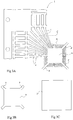
- the present invention provides for the production of a grid 1 with the external dimensions of that of a family of housings and which comprises connection pins 4 extending towards a central zone 8 as small as possible, preferably the dimensions of the smallest chip to be mounted.
- a grid 1 having a central zone 8, the size of which corresponds to the mechanical feasibility limit for the ends of the pins 4 proximal to this central zone 8, is produced by means of a mechanical punching tool, if this zone 8 cannot be as small as the smallest chip.
- This central zone 8 can be empty, but it is preferably full to ensure a certain rigidity of the grid.
- the grid 1 is associated during the mounting of a chip in the housing with a 3 ′ (FIG. 3B) or 3 "platform (FIG. 3C), the size of which depends on the size of the chip.
- the 3 ′ platform or 3 " is made separately from the grid 1.
- the center of the grid 1 is removed by cutting according to the size of the platform 3 'or 3" and therefore according to the size of the chip.
- connection of the 3 'or 3 "platform to the grid 1 is ensured by at least two straps 4' of the grid 1, the proximal ends of the center of the grid 1 are welded to the platform 3 'or 3 ".
- the center of the grid 1 is cut in a pattern which depends on the embodiment and the shape of the platform.
- FIG. 3B illustrates a first variant of a first embodiment according to which the platform 3 'has four projecting legs 9, regularly distributed in the plane of the platform 3'. These legs 9 are for example at the four corners of the platform 3 ', if it is rectangular or square as shown in FIG. 3B.
- the grid 1 is cut in a square pattern slightly greater than the square pattern in which the platform 3 ′ fits without its legs 9.
- the pattern of the cut of the grid 1 has a general shape similar to the general shape of the platform 3 'but is of a slightly larger size so that the ends of the pins 4, proximal of the platform 3', are not in contact with the latter, with the exception of the straps 4 'to which the platform 3' is welded by its legs.
- the area of the grid 1 hollowed out according to this variant is represented by the dotted line B in FIG. 3A.
- FIG. 3C illustrates a second variant of the first embodiment according to which the platform 3 "has no legs.
- the grid 1 is always cut in a pattern of size slightly larger than the pattern of the platform 3" but in leaving the straps 4 'a length greater than that of the pins 4 of the grid 1.
- the area of the grid 1 hollowed out according to this variant is represented by the dotted line C in FIG. 3A.
- connection of the straps 4 'with the platform 3' or 3 is for example carried out by spot welding by means of a laser.
- the invention makes it possible to optimize the profitability of the tools for punching the grids. Indeed, the same tool for punching grids is used for a whole family of housings comprising chips of different sizes. Only simple punching tools, therefore inexpensive, intended to perform the central cutting of the grid are associated with each type of chip.
- An advantage of the platform produced separately is that it allows the chip to be fixed to the platform before it is linked to the grid 1. This considerably limits the risks of deterioration of the grid 1, which is very fragile due to the fineness of its pins 4, considerably reducing its handling.
- the grid 1 is thus associated with the platform at the last moment for the realization of the connections of the pins 4 to the pads of the chip and the encapsulation.
- the platform can be made of a material different from that of the grid, or even have a thickness different from that of the grid. It is thus possible, for example, to choose a material for the platform (for example an alloy of iron and nickel) whose coefficient of expansion is close to that of the silicon which constitutes the chip. This is not the case for copper generally used for the grid for its electrical conductivity characteristics. Adapting the expansion of the platform to the expansion of the chip makes it possible to limit the risks of damage to the chip which can occur during the drying of the encapsulation resin or during the operation of the circuit in which the housing is installed under the effect of temperature variations, or even during welding operations (wave, oven).
- FIGS. 4A to 6B illustrate a second embodiment of the invention in which the platform plays the role of heat sink.
- a platform according to this embodiment is made of a material allowing a high thermal dissipation which is partially covered in determined zones with an insulation layer.
- this material is preferably aluminum, anodized in specific areas.
- the choice of aluminum is motivated by the fact that it is an excellent thermal conductor and that the aluminum platform can be locally masked by means of a sparing varnish which resists anodizing acids.
- the savings varnish has the characteristic of being able to be then eliminated in a weakly alkaline solution in which the layer of anodized aluminum has a chemical inertia of several minutes. This period is sufficient to remove the savings varnish.
- the thickness of the anodized zones is for example of the order of 3 to 15 micrometers.
- FIGS. 4A to 4C illustrate a first variant of a platform 3a of anodized aluminum in determined zones.
- Figures 4B and 4C are respectively sections along lines B-B 'and C-C' of the top view shown in Figure 4A.
- the platform 3a is anodized on all of its surfaces with the exception of zones 10 intended to be welded under the straps 4 'of a grid.
- the anodized zones of the platform 3a have been represented on the sectional views by a layer 11.
- Such an embodiment further simplifies the tools necessary for the central cutting of the grid and for cutting of the platform.
- the grid and the platform can now be cut according to similar patterns, the central cut of the grid being of a size slightly smaller than the size of the platform 3a.
- the ends of all pins 4, proximal to the center of the grid rest on the platform 3a, but this is not troublesome insofar as the surface of the platform 3a is anodized.
- a platform 3a as shown in Figures 4A to 4C can for example be used to receive a chip devoid of ground plane on the underside.
- FIGS. 5A and 5B illustrate a second variant of a platform 3b made of anodized aluminum in specific areas.
- Figure 5B is a section along line D-D 'of the top view shown in Figure 5A.
- the platform 3b is made of anodized aluminum.
- the non-anodized zones include zones 10 similar to those of FIG. 4A, but these zones 10 join a non-anodized central zone 12.
- a platform 3b as shown in FIGS. 5A and 5B can for example be used to receive a chip provided with a ground plane on the underside. The electrical connections of the ground plane with the outside of the box are made through zones 12 and 10 and the straps 4 'of the grid.
- FIGS. 6A and 6B illustrate a third variant of a platform 3c made of anodized aluminum in determined zones.
- Figure 6B is a section along line E-E 'of the top view shown in Figure 6A.
- the platform 3c is made of anodized aluminum.
- the non-anodized zones include zones 10 similar to those of FIG. 4A, but these zones 10 are connected together by a ring 13 also non-anodized, the central part 14 of the platform being anodized.
- a platform 3c as shown in FIGS. 6A and 6B can for example be used to receive a chip devoid of ground plane but comprising several ground pads on the upper face.
- the connecting conductive wires of the various ground studs are all attached to the ring 13 and connected with the outside of the housing via the zones 10 and the straps 4 ′ of the grid 1.
- the present invention is susceptible of various variants and modifications which will appear to those skilled in the art.
- the choice of materials constituting the grid and the platform depends on the application for which the housing is intended.
- the invention applies to any form of box.
- the grid and the platform may have distinct shapes.
Landscapes
- Cooling Or The Like Of Semiconductors Or Solid State Devices (AREA)
- Lead Frames For Integrated Circuits (AREA)
Applications Claiming Priority (2)
| Application Number | Priority Date | Filing Date | Title |
|---|---|---|---|
| FR9504065 | 1995-03-31 | ||
| FR9504065A FR2732509B1 (fr) | 1995-03-31 | 1995-03-31 | Boitier de montage d'une puce de circuit integre |
Publications (2)
| Publication Number | Publication Date |
|---|---|
| EP0735582A1 true EP0735582A1 (de) | 1996-10-02 |
| EP0735582B1 EP0735582B1 (de) | 2000-09-06 |
Family
ID=9477794
Family Applications (1)
| Application Number | Title | Priority Date | Filing Date |
|---|---|---|---|
| EP96410031A Expired - Lifetime EP0735582B1 (de) | 1995-03-31 | 1996-03-26 | Packung zur Montage eines IC-Chips |
Country Status (5)
| Country | Link |
|---|---|
| US (1) | US6049971A (de) |
| EP (1) | EP0735582B1 (de) |
| JP (1) | JPH08321576A (de) |
| DE (1) | DE69610133T2 (de) |
| FR (1) | FR2732509B1 (de) |
Families Citing this family (14)
| Publication number | Priority date | Publication date | Assignee | Title |
|---|---|---|---|---|
| US6493338B1 (en) | 1997-05-19 | 2002-12-10 | Airbiquity Inc. | Multichannel in-band signaling for data communications over digital wireless telecommunications networks |
| US6690681B1 (en) | 1997-05-19 | 2004-02-10 | Airbiquity Inc. | In-band signaling for data communications over digital wireless telecommunications network |
| US6140956A (en) | 1997-06-25 | 2000-10-31 | Cellutrac, Inc. | Vehicle tracking and security system incorporating simultaneous voice and data communication |
| US6258630B1 (en) * | 1999-02-04 | 2001-07-10 | Nec Corporation | Resin-sealed semiconductor device having island for mounting semiconductor element coupled to heat spreader |
| US7215965B2 (en) | 2001-11-01 | 2007-05-08 | Airbiquity Inc. | Facility and method for wireless transmission of location data in a voice channel of a digital wireless telecommunications network |
| US7508810B2 (en) | 2005-01-31 | 2009-03-24 | Airbiquity Inc. | Voice channel control of wireless packet data communications |
| US8014942B2 (en) * | 2005-06-15 | 2011-09-06 | Airbiquity, Inc. | Remote destination programming for vehicle navigation |
| US7924934B2 (en) | 2006-04-07 | 2011-04-12 | Airbiquity, Inc. | Time diversity voice channel data communications |
| US8594138B2 (en) | 2008-09-15 | 2013-11-26 | Airbiquity Inc. | Methods for in-band signaling through enhanced variable-rate codecs |
| US7983310B2 (en) | 2008-09-15 | 2011-07-19 | Airbiquity Inc. | Methods for in-band signaling through enhanced variable-rate codecs |
| US8036600B2 (en) | 2009-04-27 | 2011-10-11 | Airbiquity, Inc. | Using a bluetooth capable mobile phone to access a remote network |
| US8418039B2 (en) | 2009-08-03 | 2013-04-09 | Airbiquity Inc. | Efficient error correction scheme for data transmission in a wireless in-band signaling system |
| US8249865B2 (en) | 2009-11-23 | 2012-08-21 | Airbiquity Inc. | Adaptive data transmission for a digital in-band modem operating over a voice channel |
| US8848825B2 (en) | 2011-09-22 | 2014-09-30 | Airbiquity Inc. | Echo cancellation in wireless inband signaling modem |
Citations (6)
| Publication number | Priority date | Publication date | Assignee | Title |
|---|---|---|---|---|
| JPS5882540A (ja) * | 1981-11-11 | 1983-05-18 | Toshiba Corp | 樹脂封止型半導体装置 |
| EP0503072A1 (de) * | 1990-09-10 | 1992-09-16 | Fujitsu Limited | Halbleiteranordnung und ihr herstellungsverfahren |
| JPH0547986A (ja) * | 1991-08-20 | 1993-02-26 | Fujitsu Ltd | 複合型リードフレーム |
| EP0534678A2 (de) * | 1991-09-25 | 1993-03-31 | AT&T Corp. | Herstellungsverfahren für elektronische Bauteilverpackungen |
| US5256598A (en) * | 1992-04-15 | 1993-10-26 | Micron Technology, Inc. | Shrink accommodating lead frame |
| JPH06252330A (ja) * | 1993-02-23 | 1994-09-09 | Dainippon Printing Co Ltd | 配線基板用リードフレーム |
Family Cites Families (9)
| Publication number | Priority date | Publication date | Assignee | Title |
|---|---|---|---|---|
| US4079511A (en) * | 1976-07-30 | 1978-03-21 | Amp Incorporated | Method for packaging hermetically sealed integrated circuit chips on lead frames |
| JPS6070752A (ja) * | 1983-09-26 | 1985-04-22 | Fujitsu Ltd | 半導体装置の製造方法 |
| US5202288A (en) * | 1990-06-01 | 1993-04-13 | Robert Bosch Gmbh | Method of manufacturing an electronic circuit component incorporating a heat sink |
| US5161304A (en) * | 1990-06-06 | 1992-11-10 | Sgs-Thomson Microelectronics, Inc. | Method for packaging an electronic circuit device |
| US5422435A (en) * | 1992-05-22 | 1995-06-06 | National Semiconductor Corporation | Stacked multi-chip modules and method of manufacturing |
| JP2960283B2 (ja) * | 1993-06-14 | 1999-10-06 | 株式会社東芝 | 樹脂封止型半導体装置の製造方法と、この製造方法に用いられる複数の半導体素子を載置するためのリードフレームと、この製造方法によって製造される樹脂封止型半導体装置 |
| JPH077125A (ja) * | 1993-06-15 | 1995-01-10 | Shinko Electric Ind Co Ltd | 多層リードフレーム |
| JPH0738036A (ja) * | 1993-07-19 | 1995-02-07 | Fujitsu Ltd | 半導体装置の製造方法 |
| US5366933A (en) * | 1993-10-13 | 1994-11-22 | Intel Corporation | Method for constructing a dual sided, wire bonded integrated circuit chip package |
-
1995
- 1995-03-31 FR FR9504065A patent/FR2732509B1/fr not_active Expired - Fee Related
-
1996
- 1996-03-26 DE DE69610133T patent/DE69610133T2/de not_active Expired - Fee Related
- 1996-03-26 EP EP96410031A patent/EP0735582B1/de not_active Expired - Lifetime
- 1996-03-29 JP JP8076058A patent/JPH08321576A/ja active Pending
-
1997
- 1997-06-13 US US08/876,016 patent/US6049971A/en not_active Expired - Lifetime
Patent Citations (6)
| Publication number | Priority date | Publication date | Assignee | Title |
|---|---|---|---|---|
| JPS5882540A (ja) * | 1981-11-11 | 1983-05-18 | Toshiba Corp | 樹脂封止型半導体装置 |
| EP0503072A1 (de) * | 1990-09-10 | 1992-09-16 | Fujitsu Limited | Halbleiteranordnung und ihr herstellungsverfahren |
| JPH0547986A (ja) * | 1991-08-20 | 1993-02-26 | Fujitsu Ltd | 複合型リードフレーム |
| EP0534678A2 (de) * | 1991-09-25 | 1993-03-31 | AT&T Corp. | Herstellungsverfahren für elektronische Bauteilverpackungen |
| US5256598A (en) * | 1992-04-15 | 1993-10-26 | Micron Technology, Inc. | Shrink accommodating lead frame |
| JPH06252330A (ja) * | 1993-02-23 | 1994-09-09 | Dainippon Printing Co Ltd | 配線基板用リードフレーム |
Non-Patent Citations (3)
| Title |
|---|
| PATENT ABSTRACTS OF JAPAN vol. 007, no. 178 (E - 191) 6 August 1983 (1983-08-06) * |
| PATENT ABSTRACTS OF JAPAN vol. 017, no. 344 (E - 1390) 29 June 1993 (1993-06-29) * |
| PATENT ABSTRACTS OF JAPAN vol. 018, no. 643 (E - 1640) 7 December 1994 (1994-12-07) * |
Also Published As
| Publication number | Publication date |
|---|---|
| JPH08321576A (ja) | 1996-12-03 |
| US6049971A (en) | 2000-04-18 |
| EP0735582B1 (de) | 2000-09-06 |
| FR2732509A1 (fr) | 1996-10-04 |
| DE69610133T2 (de) | 2001-04-12 |
| DE69610133D1 (de) | 2000-10-12 |
| FR2732509B1 (fr) | 1997-06-13 |
Similar Documents
| Publication | Publication Date | Title |
|---|---|---|
| EP0239494B1 (de) | Gehäuse für integrierte Schaltung | |
| EP0735582B1 (de) | Packung zur Montage eines IC-Chips | |
| EP0923130B1 (de) | Elektronische Schaltung, insbesondere für implantierbare aktive medizinische Vorrichtung, wie ein Herzstimulator oder -defibrillator, und deren Herstellungsmethode | |
| EP0321340B1 (de) | Halter für elektronische Komponenten, insbesondere für Speicherkarten und auf solche Weise hergestelltes Produkt | |
| FR2762929A1 (fr) | Boitier de semi-conducteur ayant un element semi-conducteur, une structure de fixation de boitier de semi-conducteur montee sur une plaquette de circuits imprimes, et procede d'assemblage de boitier de semi-conducteur | |
| FR2518811A1 (fr) | Dispositif a circuit integre en conteneur de ceramique | |
| EP0593330B1 (de) | 3D-Verbindungsverfahren für Gehäuse von elektronischen Bauteilen und resultierendes 3D-Bauteil | |
| EP0638929B1 (de) | Wärmesenke für Plastikpackung | |
| EP0178977A1 (de) | Ein in ein Plastikgehäuse montiertes Halbleiterbauelement und Verfahren zu seiner Herstellung | |
| FR2547112A1 (fr) | Procede de realisation d'un circuit hybride et circuit hybride logique ou analogique | |
| CA2915853C (fr) | Capteur differentiel de temperature | |
| EP0068946B1 (de) | Verfahren zum Herstellen eines Einheitsbauelementes mit einer Oszillatordiode und einer Varaktordiode, und frequenzabstimmbare Sender mit solchem Einheitsbauelement | |
| FR2571895A1 (fr) | Procede de montage de deux composants semi-conducteurs dans un boitier commun et dispositif obtenu par ce procede | |
| FR2748856A1 (fr) | Dispositif diode a semiconducteur a montage en surface | |
| FR2861217A1 (fr) | Dispositif optique pour boitier semi-conducteur optique et procede de fabrication. | |
| EP0368741A1 (de) | Integrierter Schaltungsträger und Verfahren zum Herstellen desselben, integrierte Schaltung, angepasst an den Träger und resultierende Gehäuse | |
| EP0221809B1 (de) | Hybridschaltung und Verfahren zum Herstellen einer solchen Schaltung | |
| EP3477698B1 (de) | Integrierter schaltkreis in einem qfn-gehäuse | |
| FR3123778A1 (fr) | Procédé de fabrication d’un circuit imprimé intégrant un composant électronique et module de carte à puce obtenu par ledit procédé. | |
| FR2651923A1 (fr) | Circuit integre de puissance. | |
| FR2664097A1 (fr) | Boitier de circuit integre et son procede de fabrication. | |
| WO2002058107A2 (fr) | Procede de fabrication d'un boitier semi-conducteur optique et boitier semi-conducteur optique | |
| EP4625478A1 (de) | Verfahren zum zusammenbau einer integrierten schaltung in vertikaler richtung und bauelement mit integrierter vertikaler schaltung | |
| FR3162911A1 (fr) | Fabrication d’un module de puissance | |
| FR2734948A1 (fr) | Boitier d'encapsulation a reseau de boules de soudure et procede d'encapsulation. |
Legal Events
| Date | Code | Title | Description |
|---|---|---|---|
| PUAI | Public reference made under article 153(3) epc to a published international application that has entered the european phase |
Free format text: ORIGINAL CODE: 0009012 |
|
| AK | Designated contracting states |
Kind code of ref document: A1 Designated state(s): DE FR GB IT |
|
| 17P | Request for examination filed |
Effective date: 19970311 |
|
| 17Q | First examination report despatched |
Effective date: 19980625 |
|
| RAP3 | Party data changed (applicant data changed or rights of an application transferred) |
Owner name: STMICROELECTRONICS S.A. |
|
| GRAG | Despatch of communication of intention to grant |
Free format text: ORIGINAL CODE: EPIDOS AGRA |
|
| GRAG | Despatch of communication of intention to grant |
Free format text: ORIGINAL CODE: EPIDOS AGRA |
|
| GRAH | Despatch of communication of intention to grant a patent |
Free format text: ORIGINAL CODE: EPIDOS IGRA |
|
| GRAH | Despatch of communication of intention to grant a patent |
Free format text: ORIGINAL CODE: EPIDOS IGRA |
|
| GRAA | (expected) grant |
Free format text: ORIGINAL CODE: 0009210 |
|
| AK | Designated contracting states |
Kind code of ref document: B1 Designated state(s): DE FR GB IT |
|
| REF | Corresponds to: |
Ref document number: 69610133 Country of ref document: DE Date of ref document: 20001012 |
|
| GBT | Gb: translation of ep patent filed (gb section 77(6)(a)/1977) |
Effective date: 20000925 |
|
| ITF | It: translation for a ep patent filed | ||
| PLBE | No opposition filed within time limit |
Free format text: ORIGINAL CODE: 0009261 |
|
| STAA | Information on the status of an ep patent application or granted ep patent |
Free format text: STATUS: NO OPPOSITION FILED WITHIN TIME LIMIT |
|
| 26N | No opposition filed | ||
| REG | Reference to a national code |
Ref country code: GB Ref legal event code: IF02 |
|
| PGFP | Annual fee paid to national office [announced via postgrant information from national office to epo] |
Ref country code: DE Payment date: 20040408 Year of fee payment: 9 |
|
| PGFP | Annual fee paid to national office [announced via postgrant information from national office to epo] |
Ref country code: FR Payment date: 20050308 Year of fee payment: 10 |
|
| PGFP | Annual fee paid to national office [announced via postgrant information from national office to epo] |
Ref country code: GB Payment date: 20050323 Year of fee payment: 10 |
|
| PG25 | Lapsed in a contracting state [announced via postgrant information from national office to epo] |
Ref country code: IT Free format text: LAPSE BECAUSE OF NON-PAYMENT OF DUE FEES Effective date: 20050326 |
|
| PG25 | Lapsed in a contracting state [announced via postgrant information from national office to epo] |
Ref country code: DE Free format text: LAPSE BECAUSE OF NON-PAYMENT OF DUE FEES Effective date: 20051001 |
|
| PG25 | Lapsed in a contracting state [announced via postgrant information from national office to epo] |
Ref country code: GB Free format text: LAPSE BECAUSE OF NON-PAYMENT OF DUE FEES Effective date: 20060326 |
|
| GBPC | Gb: european patent ceased through non-payment of renewal fee |
Effective date: 20060326 |
|
| REG | Reference to a national code |
Ref country code: FR Ref legal event code: ST Effective date: 20061130 |
|
| PG25 | Lapsed in a contracting state [announced via postgrant information from national office to epo] |
Ref country code: FR Free format text: LAPSE BECAUSE OF NON-PAYMENT OF DUE FEES Effective date: 20060331 |