EP0735584A2 - Integrierte Schaltung in Mehrlagen-Verbindungstechnik - Google Patents
Integrierte Schaltung in Mehrlagen-Verbindungstechnik Download PDFInfo
- Publication number
- EP0735584A2 EP0735584A2 EP96301889A EP96301889A EP0735584A2 EP 0735584 A2 EP0735584 A2 EP 0735584A2 EP 96301889 A EP96301889 A EP 96301889A EP 96301889 A EP96301889 A EP 96301889A EP 0735584 A2 EP0735584 A2 EP 0735584A2
- Authority
- EP
- European Patent Office
- Prior art keywords
- conductors
- conductor
- level
- power supply
- block
- Prior art date
- Legal status (The legal status is an assumption and is not a legal conclusion. Google has not performed a legal analysis and makes no representation as to the accuracy of the status listed.)
- Withdrawn
Links
Images


Classifications
-
- H—ELECTRICITY
- H10—SEMICONDUCTOR DEVICES; ELECTRIC SOLID-STATE DEVICES NOT OTHERWISE PROVIDED FOR
- H10D—INORGANIC ELECTRIC SEMICONDUCTOR DEVICES
- H10D84/00—Integrated devices formed in or on semiconductor substrates that comprise only semiconducting layers, e.g. on Si wafers or on GaAs-on-Si wafers
-
- H—ELECTRICITY
- H10—SEMICONDUCTOR DEVICES; ELECTRIC SOLID-STATE DEVICES NOT OTHERWISE PROVIDED FOR
- H10W—GENERIC PACKAGES, INTERCONNECTIONS, CONNECTORS OR OTHER CONSTRUCTIONAL DETAILS OF DEVICES COVERED BY CLASS H10
- H10W20/00—Interconnections in chips, wafers or substrates
- H10W20/40—Interconnections external to wafers or substrates, e.g. back-end-of-line [BEOL] metallisations or vias connecting to gate electrodes
- H10W20/41—Interconnections external to wafers or substrates, e.g. back-end-of-line [BEOL] metallisations or vias connecting to gate electrodes characterised by their conductive parts
- H10W20/427—Power or ground buses
Definitions
- the present invention relates to an integrated circuit having multiple conductor levels for interconnection of circuitry.
- Integrated circuits typically utilize multiple levels of conductors for distributing power supply voltages, as well as operational signals, between various portions of the IC.
- the conductors are most typically metal in the case of power supply distribution, usually aluminum, tungsten, titanium or gold, with still others (e.g., copper) being possible. These provide high conductivity and hence low voltage drop as power supply current flows.
- signal conductors an even wider range of materials is often used, including doped polysilicon, metal silicides and metal nitrides in addition to the metals noted above.
- Conductors are formed by lithographically patterning a given level of conductive material, to form conductive lines as viewed from above an IC substrate.
- the conductor levels are separated from one another by dielectric layers for electrical insulation.
- the dielectric is often a glass (e.g., silicon dioxide including phosphorus and/or boron) at the lowest level (i.e., the level nearest the semiconductor substrate).
- silicon dioxide is typical as an interlevel dielectric between the higher conductor levels (i.e., the levels overlying the lower conductor levels).
- the conductors may communicate by means of openings in the dielectric layers, referred to as "vias", with other conductor levels.
- the conductors also may communicate to doped device regions in the semiconductor substrate by means of openings in the lowest dielectric level, referred to as "contact windows".
- Fig. 1 One typical form of conductor layout is illustrated in Fig. 1, wherein the metal conductors 109 - 115 lie in wiring channels between various ones of the functional circuit blocks 101 - 108.
- the metal conductors may extend from the wiring channels into the circuit blocks as indicated. Usually only the metal conductors are located within the wiring channels, while within a given circuit block, both the metal conductors and the polysilicon/silicide conductors are used.
- the circuit blocks shown are typical for use in a digital signal processor (DSP), which is chosen to be illustrative of the prior art.
- DSP digital signal processor
- a DSP typically includes a central processing unit (CPU) 101 that includes arithmetic address unit (AAU) 102, a sequence control unit (SCU) 103, a digital arithmetic unit (DAU) 104, and sometimes also a bit manipulation unit (BMU) 105.
- the CPU 101 communicates with a random access memory (RAM) 106, a read-only memory (ROM) 107, and an input/output (IO) unit 108.
- RAM random access memory
- ROM read-only memory
- IO input/output
- the long conductors in the wiring channels e.g., 109, 110, 111, 112, 113, 114, 115
- the short stubs that feed into the modules e.g., 116, 117, 118, 119
- conductors (109, 111) turn the corner around a block (106) to change from a horizontal to a vertical conductor, while avoiding crossing over of another conductor.
- some conductors cross over other conductors.
- conductor 110 connects to conductor 113 by means of a cross-under portion 120 that is formed in metal 1, and connected by means of vias 121 and 122. This allows conductor 112 to cross-over without connection to conductor 110.
- Still another example is cross-under conductor 123. Note that the boundaries of the circuit blocks are shown as dotted lines. These boundaries may include power and ground (V DD and V SS ) conductors, typically in metal 2.
- V DD was used on two sides of a circuit block
- V SS was used on the other two sides.
- a V DD encompassed an entire circuit block
- V SS encompassed another circuit block.
- the stubs that feed V DD and/or V SS into the modules are then typically implemented in metal 2. At these places the interconnect wires cross under in metal 1.
- the power and ground conductors are formed in the wiring channels parallel to the signal conductors. These power supply conductors then turn into the circuit blocks (i.e., at right angles to the wiring channels), and are jumpered down by vias to the metal 2 and metal 1 conductors as required inside the circuit blocks.
- Lower and upper conductor levels bound a circuit block on at least one side and provide for power supply voltage distribution to the circuitry in the circuit block.
- the lower and upper conductor levels also provide for first and second groups of parallel signal conductors in wiring channels between circuit blocks.
- An intermediate conductor level is located between the lower and upper conductor levels, and conducts power supply voltages between adjacent circuit blocks.
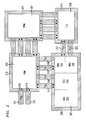
- FIG. 2 an illustrative embodiment shows how circuit blocks that implement functionality comparable to those shown in Fig. 1 may be provided with power supply voltages by the inventive technique.
- the illustrated circuit blocks 201, 206, 207 and 208 are bounded by two overlying levels of conductors, shown collectively in top view with associated conductor vias.
- the CPU circuit block 201 comprising circuit sub-blocks 202-205, is bounded by conductor 209.
- Each conductor bounding a circuit block comprises an upper conductor seen in Fig. 2, and also a lower conductor that is hidden from view by the upper conductor.
- the lower conductor is indicated as a "prime" of the corresponding upper conductor.
- the upper conductor is connected to a source of a first power supply voltage, illustratively V SS
- the lower conductor is connected to a source of a second power supply voltage, illustratively V DD , as discussed further below.
- intermediate level conductors are used to distribute power supply voltages between blocks, as discussed in detail below.
- the term "intermediate power supply conductor” means a power supply conductor that is formed from an intermediate conductor level.
- An “intermediate conductor level” is a conductor level above the lower conductor level and below the upper conductor level with respect to the semiconductor substrate on which the integrated circuit is formed.
- intermediate level conductors 213 and 214 on the outer periphery of block 206 supply voltages V SS and V DD respectively from power supply bondpads (not shown) to the upper conductor 210 and lower conductor 210' through vias 215 and 216, respectively.
- the vias 215 connect the upper conductor 210 to the intermediate V SS conductor 213, and hence are shown as solid circles in Fig. 2.
- the vias 216 connect the lower conductor 210' to the intermediate V DD conductor 214; hence the vias 216 are shown as open circles to indicate that they are hidden from view.
- intermediate power supply conductors that connect the adjacent blocks, providing conduction of power supply voltages to the upper and lower conductors that bound the blocks.
- the signal conductors are omitted from the wiring channels in Fig. 2 for clarity of illustration).
- the intermediate power supply conductor 221 provides conduction of the V SS voltage between the upper conductor 209 (block 201) and the upper conductor 212 (block 208).
- the intermediate power supply conductor 222 provides conduction of the V DD voltage between the lower conductor 209' (block 201) and the lower conductor 212' (block 208).
- intermediate power supply conductors 217, 219 provide connection of the upper (V SS ) conductors of adjacent blocks 201 and 206
- intermediate power supply conductors 218, 220 provide connection of the lower (V DD ) conductors of adjacent blocks 201 and 206, thereby distributing the V SS and V DD power supply voltages respectively.
- the upper and lower conductors of block 207 are similarly connected to the upper and lower conductors of adjacent blocks 206 and 208 by intermediate power supply conductors, not numbered for clarity of illustration. In this manner, the power supply may be efficiently distributed to the various circuit blocks.
- the upper and lower conductors that bound a circuit block serve as distribution busses for power supply voltages to circuitry within their associated blocks.
- the distribution of power supply voltages within a given block may be accomplished by means of distribution conductors (not shown) in any desired conductor arrangement.
- distribution conductors not shown
- a grid of horizontal and vertical (as defined by Fig. 2) distribution conductors that run across a given circuit block is used.
- the intermediate conductor level e.g., metal 2 may be used to provide spaced V DD and V SS power distribution conductors that run horizontally across a given circuit block.
- These horizontal distribution conductors may directly connect (i.e., without vias) to the intermediate power supply conductors that run across the wiring channels from the adjacent circuit blocks.
- the upper conductor level e.g., metal 3
- the upper conductor level e.g., metal 3
- V DD and V SS power distribution conductors that run vertically across a given circuit block.
- These vertical distribution conductors that carry V SS may then connect directly to the upper conductor that bounds the given circuit block, and the vertical distribution conductors that carry V DD may then connect by means of vias down to the lower conductor that bounds the given circuit block.
- various other distribution arrangements are possible for use with the present invention.
- Fig. 3 wherein signal conductors in the routing channels are illustrated. These signal conductors are formed from the upper and lower conductor levels. (The intermediate power supply conductors discussed above are omitted from the wiring channels in Fig. 3 for clarity of illustration).
- signal conductors of the upper conductor level may directly overlie signal conductors of the lower conductor level (the "lower signal conductors") in a given wiring channel.
- the lower signal conductor that underlies a given upper signal conductor is indicated by a prime in discussions herein. For example, upper signal conductor 301 is illustrated, with lower signal conductor 301' lying thereunder.
- a feed 302 in the upper conductor level (e.g., metal 3) may be used to bring conductor 301 into the RAM block 206.
- a feed 303 in the lower conductor level (e.g., metal 1) may be used to bring conductor 301' into the RAM block 206.
- the upper and lower signal conductors are separated by the intermediate power supply conductors (Fig. 2).
- These intermediate power supply conductors whether V DD or V SS , are at ground potential with respect to the alternating-current (AC) signals conducted by the upper and lower signal conductors. Therefore, a high degree of shielding of the upper signal conductors from the lower signal conductors (and vice-versa) in a wiring channel is accomplished using the intermediate level conductors for power supply distribution.
- One advantage of this shielding is that the simulation of circuit operation may be more accurately accomplished using computer-aided circuit simulators. This is because the signals in the upper and lower conductors may be considered to not interact, or at least interact to a significantly reduced extent, in integrated circuits implementing the present invention.
- the intermediate power supply conductors cover at least 50 percent, and preferably at least 80 percent, of the area in the wiring channels.
- V SS When using a p-type silicon substrate connected to V SS , it is desirable to connect the lowest conductor level (e.g., metal 1) that bounds a circuit block to V DD , in order to increase total capacitance and hence reduce noise in the power supply, and also improve electrostatic discharge (ESD) protection. Also, this allows the use of the upper conductor level (e.g., metal 3) to connect to V SS . That is desirable in the typical case that metal 3 is relatively thicker than metal 1 or metal 2.
- the V SS and V DD conductors in the intermediate level (e.g, metal 2) typically alternate, which facilitates power supply connections within the bounded circuit block. However, this is not necessarily the case, and occasionally two (or more) adjacent intermediate level conductors will carry either both V DD or V SS .
- the above illustrative embodiment has shown all adjacent sides of the circuit blocks interconnected by the intermediate power supply conductors, that is of course not possible for the edges of the blocks that are not adjacent other circuit blocks. In some cases, only a single edge of a circuit block is bounded by power supply conductors according to the inventive technique.
- still other portions of the integrated circuit may use conventional conductor placement techniques, although of course not obtaining the advantages of the inventive technique in those portions of the circuitry. Thus, the inventive technique may be practiced on only two adjacent blocks if desired.
- the illustrative embodiment has shown the upper conductor bounding a given block being connected to an upper conductor bounding the adjacent block (and similarly showing the lower bounding conductors connected). However, that is not necessary, since the intermediate power supply conductors may connect an upper conductor bounding a given block to the lower conductor bounding an adjacent block while still obtaining various of the above-noted advantages. Still other variations are possible.
Landscapes
- Design And Manufacture Of Integrated Circuits (AREA)
- Semiconductor Integrated Circuits (AREA)
- Structure Of Printed Boards (AREA)
Applications Claiming Priority (2)
| Application Number | Priority Date | Filing Date | Title |
|---|---|---|---|
| US08/413,527 US5663677A (en) | 1995-03-30 | 1995-03-30 | Integrated circuit multi-level interconnection technique |
| US413527 | 1995-03-30 |
Publications (2)
| Publication Number | Publication Date |
|---|---|
| EP0735584A2 true EP0735584A2 (de) | 1996-10-02 |
| EP0735584A3 EP0735584A3 (de) | 1997-12-29 |
Family
ID=23637567
Family Applications (1)
| Application Number | Title | Priority Date | Filing Date |
|---|---|---|---|
| EP96301889A Withdrawn EP0735584A3 (de) | 1995-03-30 | 1996-03-20 | Integrierte Schaltung in Mehrlagen-Verbindungstechnik |
Country Status (4)
| Country | Link |
|---|---|
| US (1) | US5663677A (de) |
| EP (1) | EP0735584A3 (de) |
| JP (1) | JP3258232B2 (de) |
| KR (1) | KR100390667B1 (de) |
Families Citing this family (13)
| Publication number | Priority date | Publication date | Assignee | Title |
|---|---|---|---|---|
| JP3438803B2 (ja) * | 1996-07-05 | 2003-08-18 | 富士通株式会社 | 電源ノイズ除去方法及び半導体装置 |
| JP3373753B2 (ja) * | 1997-03-28 | 2003-02-04 | 株式会社東芝 | 超高周波帯無線通信装置 |
| US6118334A (en) * | 1997-05-19 | 2000-09-12 | Kabushiki Kaisha Toshiba | Semiconductor integrated circuit and power supply routing method and system |
| JPH1140736A (ja) * | 1997-07-16 | 1999-02-12 | Nec Ic Microcomput Syst Ltd | 半導体装置 |
| US6114903A (en) * | 1998-01-14 | 2000-09-05 | Lsi Logic Corporation | Layout architecture for core I/O buffer |
| US6307252B1 (en) | 1999-03-05 | 2001-10-23 | Agere Systems Guardian Corp. | On-chip shielding of signals |
| US6388332B1 (en) | 1999-08-10 | 2002-05-14 | Philips Electronics North America Corporation | Integrated circuit power and ground routing |
| JP4748867B2 (ja) * | 2001-03-05 | 2011-08-17 | パナソニック株式会社 | 集積回路装置 |
| US7324364B2 (en) * | 2006-02-27 | 2008-01-29 | Agere Systems Inc. | Layout techniques for memory circuitry |
| US7301828B2 (en) * | 2006-02-27 | 2007-11-27 | Agere Systems Inc. | Decoding techniques for read-only memory |
| US9076848B2 (en) | 2013-03-12 | 2015-07-07 | International Business Machines Corporation | Semiconductor device channels |
| US9111935B2 (en) | 2013-03-12 | 2015-08-18 | International Business Machines Corporation | Multiple-patterned semiconductor device channels |
| US9099471B2 (en) | 2013-03-12 | 2015-08-04 | International Business Machines Corporation | Semiconductor device channels |
Family Cites Families (11)
| Publication number | Priority date | Publication date | Assignee | Title |
|---|---|---|---|---|
| JP2606845B2 (ja) * | 1987-06-19 | 1997-05-07 | 富士通株式会社 | 半導体集積回路 |
| JPH077809B2 (ja) * | 1988-03-29 | 1995-01-30 | 株式会社東芝 | 集積回路 |
| JPH01297839A (ja) * | 1988-05-26 | 1989-11-30 | Toshiba Corp | 半導体装置 |
| JP2668981B2 (ja) * | 1988-09-19 | 1997-10-27 | 富士通株式会社 | 半導体集積回路 |
| JPH02163960A (ja) * | 1988-12-16 | 1990-06-25 | Toshiba Corp | 半導体装置 |
| JPH0727968B2 (ja) * | 1988-12-20 | 1995-03-29 | 株式会社東芝 | 半導体集積回路装置 |
| JPH02268439A (ja) * | 1989-04-10 | 1990-11-02 | Hitachi Ltd | 半導体集積回路装置 |
| JP2510747B2 (ja) * | 1990-02-26 | 1996-06-26 | 株式会社日立製作所 | 実装基板 |
| JPH0410624A (ja) * | 1990-04-27 | 1992-01-14 | Hitachi Ltd | 半導体集積回路 |
| JP2742735B2 (ja) * | 1991-07-30 | 1998-04-22 | 三菱電機株式会社 | 半導体集積回路装置およびそのレイアウト設計方法 |
| US5416431A (en) * | 1994-03-21 | 1995-05-16 | At&T Corp. | Integrated circuit clock driver having improved layout |
-
1995
- 1995-03-30 US US08/413,527 patent/US5663677A/en not_active Expired - Lifetime
-
1996
- 1996-03-20 EP EP96301889A patent/EP0735584A3/de not_active Withdrawn
- 1996-03-26 JP JP06956796A patent/JP3258232B2/ja not_active Expired - Lifetime
- 1996-03-29 KR KR1019960009149A patent/KR100390667B1/ko not_active Expired - Lifetime
Also Published As
| Publication number | Publication date |
|---|---|
| JP3258232B2 (ja) | 2002-02-18 |
| US5663677A (en) | 1997-09-02 |
| EP0735584A3 (de) | 1997-12-29 |
| JPH08274424A (ja) | 1996-10-18 |
| KR100390667B1 (ko) | 2003-10-30 |
| KR960036034A (ko) | 1996-10-28 |
Similar Documents
| Publication | Publication Date | Title |
|---|---|---|
| US5663677A (en) | Integrated circuit multi-level interconnection technique | |
| US4928160A (en) | Gate isolated base cell structure with off-grid gate polysilicon pattern | |
| US6858939B1 (en) | Integrated circuit diagonal wiring architectures with zag conductors | |
| US5650653A (en) | Microelectronic integrated circuit including triangular CMOS "nand" gate device | |
| US6839882B2 (en) | Method and apparatus for design of integrated circuits | |
| EP0203025B1 (de) | Gattermatrix mit verminderter Isolation | |
| US6479845B2 (en) | Pattern for routing power and ground for an integrated circuit chip | |
| WO1987000969A1 (en) | Three-level interconnection scheme for integrated circuits | |
| EP0405460A2 (de) | Halbleitervorrichtung unter Verwendung eines Standardzellen-Systems | |
| US5229629A (en) | Semiconductor integrated circuit having improved cell layout | |
| US5416431A (en) | Integrated circuit clock driver having improved layout | |
| JPH0127578B2 (de) | ||
| US6842886B2 (en) | Basic cell of gate array semiconductor device, gate array semiconductor device, and layout method for gate array semiconductor device | |
| CN101479848A (zh) | 供电网络 | |
| JP4494537B2 (ja) | スタンダードセル方式の半導体集積回路の配線設計方法 | |
| US6005264A (en) | Microelectronic integrated circuit including hexagonal CMOS "NAND" gate device | |
| JP2997479B2 (ja) | ゲートアレイ | |
| JP2679034B2 (ja) | 半導体集積装置 | |
| JPS59135744A (ja) | マスタスライス方式の半導体集積回路装置 | |
| JPH0250626B2 (de) | ||
| WO2025169464A1 (ja) | 半導体装置 | |
| WO2024214205A1 (ja) | 半導体装置 | |
| EP0288688A2 (de) | Poröser Schaltungsmacro für integrierte Halbleiterschaltungen | |
| JP2964765B2 (ja) | 多層配線層を用いた半導体集積回路 | |
| EP0702849A1 (de) | Flexcell-gate-array |
Legal Events
| Date | Code | Title | Description |
|---|---|---|---|
| PUAI | Public reference made under article 153(3) epc to a published international application that has entered the european phase |
Free format text: ORIGINAL CODE: 0009012 |
|
| AK | Designated contracting states |
Kind code of ref document: A2 Designated state(s): DE FR GB IT |
|
| PUAL | Search report despatched |
Free format text: ORIGINAL CODE: 0009013 |
|
| AK | Designated contracting states |
Kind code of ref document: A3 Designated state(s): DE FR GB IT |
|
| 17P | Request for examination filed |
Effective date: 19980618 |
|
| 17Q | First examination report despatched |
Effective date: 20020719 |
|
| STAA | Information on the status of an ep patent application or granted ep patent |
Free format text: STATUS: THE APPLICATION IS DEEMED TO BE WITHDRAWN |
|
| 18D | Application deemed to be withdrawn |
Effective date: 20021130 |