EP0735669A2 - Circuits différentiels à capacités commutées - Google Patents
Circuits différentiels à capacités commutées Download PDFInfo
- Publication number
- EP0735669A2 EP0735669A2 EP96102657A EP96102657A EP0735669A2 EP 0735669 A2 EP0735669 A2 EP 0735669A2 EP 96102657 A EP96102657 A EP 96102657A EP 96102657 A EP96102657 A EP 96102657A EP 0735669 A2 EP0735669 A2 EP 0735669A2
- Authority
- EP
- European Patent Office
- Prior art keywords
- coupled
- clock signal
- phase
- capacitor
- capacitors
- Prior art date
- Legal status (The legal status is an assumption and is not a legal conclusion. Google has not performed a legal analysis and makes no representation as to the accuracy of the status listed.)
- Granted
Links
Images

Classifications
-
- H—ELECTRICITY
- H03—ELECTRONIC CIRCUITRY
- H03F—AMPLIFIERS
- H03F3/00—Amplifiers with only discharge tubes or only semiconductor devices as amplifying elements
- H03F3/005—Amplifiers with only discharge tubes or only semiconductor devices as amplifying elements using switched capacitors, e.g. dynamic amplifiers; using switched capacitors as resistors in differential amplifiers
-
- H—ELECTRICITY
- H03—ELECTRONIC CIRCUITRY
- H03K—PULSE TECHNIQUE
- H03K17/00—Electronic switching or gating, i.e. not by contact-making and –breaking
-
- H—ELECTRICITY
- H03—ELECTRONIC CIRCUITRY
- H03F—AMPLIFIERS
- H03F3/00—Amplifiers with only discharge tubes or only semiconductor devices as amplifying elements
- H03F3/45—Differential amplifiers
- H03F3/45071—Differential amplifiers with semiconductor devices only
- H03F3/45479—Differential amplifiers with semiconductor devices only characterised by the way of common mode signal rejection
Definitions
- This invention relates to switched capacitor differential circuits.
- Switched capacitor differential circuits are generally used to provide differential inputs to operational amplifiers, and can be connected in the form of a feedback circuit between the output of the amplifier and its inputs.
- a known system includes a switched capacitor circuit 20 for switching differential inputs Vinp1 and Vinp2 into first and second inputs A and B of an operational amplifier 32.
- Switched capacitor circuit 20 receives two control inputs consisting of a first phase control clock signal PHI0 and a second phase control clock signal PHI1 that is non-overlapping with the first phase control clock signal PHI0.
- the switched capacitor circuit 20 has a first input coupled to receive input signal Vinp1 and a second input coupled to receive input signal Vinp2 and a third input coupled to receive an analog ground signal AG.
- Analog ground AG is a voltage reference relative to which the input signals Vinp1 and Vinp2 change.
- the switched capacitor circuit 20 has a first output coupled to the first input A of the amplifier 32 and a second output coupled to the second input B of the amplifier 32.
- Switched capacitor circuit 20 includes a first pair of switching transistors 22 and 23 which both have their gate electrodes connected to the first phase control clock signal PHI0, their respective source electrodes connected to the first and second inputs, respectively, and their respective drain electrodes connected to respective first electrodes of first and second respective capacitors 30 and 31.
- a second pair of switching transistors 24 and 25 both have their gate electrodes connected to the second phase control clock signal PHI1, their respective source electrodes connected to the first and second outputs, respectively, and their respective drain electrodes connected to respective second electrodes of the first and second respective capacitors 30 and 31.
- a third pair of switching transistors 28 and 29 have their gate electrodes coupled to the second phase control clock signal PHI1, their source electrodes coupled to the third input AG and their respective drain electrodes coupled to the respective first electrodes of the respective capacitors 30 and 31.
- a fourth pair of switching transistors 26 and 27 have their gate electrodes coupled to the first phase control clock signal PHI0, their source electrodes coupled to the third input AG and their respective drain electrodes coupled to the respective second electrodes of the respective capacitors 30 and 31.
- the switched capacitor circuit 20 charges capacitor 30 from the first input Vinp1, and capacitor 31 from the second input Vinp2, during an active period of the first phase control clock signal PHI0.
- capacitor 30 is discharged to the analog ground AG and its charge transferred to the first output, and the charge on capacitor 31 is similarly transferred to the second output.
- the source-drain ON resistance is also changing according to the oinput signal. Therefore, the RC constant for charging the capacitors also changes according to the input signal.
- the present invention therefore seeks to provide a switched capacitor differential circuit which overcomes, or at least reduces the above-mentioned problems of the prior art.
- the invention provides a switched capacitor differential circuit comprising first and second differential inputs coupled to respective first and second differential outputs via respective first and second signal paths, each signal path including a coupling capacitor and a first switching device between the input and the coupling capacitor and a second switching device between the coupling capacitor and the output, the control electrodes of the first switching devices of both paths being coupled together to switch at a first phase of a clock signal and the control electrodes of the second switching devices of both paths being coupled together to switch at a second phase of the clock signal non-overlapping with the first phase, a first comon mode capacitor coupled between the first input and a common mode node and a second common mode capacitor coupled between the second input and the common mode node, the common mode node being coupled via a pair of switches to the first and second signal paths between the coupling capacitors and the second switching devices, the switches being arranged to conduct during the first phase of the clock signal and not conduct during the second phase of the clock signal.
- the switches comprise a pair of transistors whose control electrodes are coupled to the control electrodes of the first switching devices.
- the circuit preferably further includes a switchable coupling path coupling the two signal paths between the coupling capacitors and the first switching devices, the coupling path being switched to conduct during the second phase of the clock signal and not to conduct during the first phase of the clock signal.
- the coupling path is coupled to a ground reference potential.
- the coupling path is preferably switched by a pair of switching devices whose control electrodes are coupled to the control electrodes of the second switching transistors.
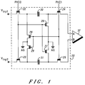
- the switching capacitor differential circuit 1 comprises a switching circuit 10 and a common mode circuit 11.
- the switching circuit 10 switches differential input signals Vinp1 and Vinp2 into first and second inputs A and B of an operational amplifier 12.
- Switching circuit 10 receives two control inputs consisting of a first phase control clock signal PHI0 and a second phase control clock signal PHI1 that is non-overlapping with the first phase control clock signal PHI0.
- the switching circuit 10 has a first input coupled to receive input signal Vinp1 and a second input coupled to receive input signal Vinp2 and a third input coupled to receive an analog ground signal AG.
- Analog ground AG is a voltage reference relative to which the input signals Vinp1 and Vinp2 change.
- the switching circuit 10 has a first output coupled to a first input A of an operational amplifier 12 and a second output coupled to a second input B of the amplifier 12.
- Switching circuit 10 includes a first pair of switching transistors 2 and 3 which both have their gate electrodes connected to the first phase control clock signal PHI0, their respective source electrodes connected to the first and second inputs, respectively, and their respective drain electrodes connected to respective first electrodes of first and second respective capacitors 13 and 14.
- a second pair of switching transistors 4 and 5 both have their gate electrodes connected to the second phase control clock signal PHI1, their respective source electrodes connected to the first and second outputs, respectively, and their respective drain electrodes connected to respective second electrodes of the first and second respective capacitors 13 and 14.
- a third pair of switching transistors 8 and 9 have their gate electrodes coupled to the second phase control clock signal PHI1, their source electrodes coupled to the third input AG and their respective drain electrodes coupled to the respective first electrodes of the respective capacitors 13 and 14.
- a fourth pair of switching transistors 6 and 7 have their gate electrodes coupled to the first phase control clock signal PHI0, their respective drain electrodes coupled to the respective second electrodes of the respective capacitors 13 and 14 and their source electrodes coupled to a node 15.
- the common mode circuit 11 includes a pair of capacitors 16 and 17. A first input of the common mode circuit 11 is coupled to the first electrode of capacitor 16 so as to receive input signal Vinp1 and a second input of the common mode circuit 11 is coupled to the first electrode of capacitor 17 so as to receive input signal Vinp2. The second electrodes of the two capacitors 16 and 17 are coupled together to form the output of the common mode circuit 11, which output is coupled to the node 15.
- the common mode circuit 11 thus provides an AC average of its first and second inputs on its output.
Landscapes
- Engineering & Computer Science (AREA)
- Power Engineering (AREA)
- Filters That Use Time-Delay Elements (AREA)
- Amplifiers (AREA)
Applications Claiming Priority (2)
| Application Number | Priority Date | Filing Date | Title |
|---|---|---|---|
| GB9506139 | 1995-03-25 | ||
| GB9506139A GB2299472B (en) | 1995-03-25 | 1995-03-25 | Switched capacitor differential circuits |
Publications (3)
| Publication Number | Publication Date |
|---|---|
| EP0735669A2 true EP0735669A2 (fr) | 1996-10-02 |
| EP0735669A3 EP0735669A3 (fr) | 1998-09-16 |
| EP0735669B1 EP0735669B1 (fr) | 2002-06-05 |
Family
ID=10771908
Family Applications (1)
| Application Number | Title | Priority Date | Filing Date |
|---|---|---|---|
| EP96102657A Expired - Lifetime EP0735669B1 (fr) | 1995-03-25 | 1996-02-22 | Circuits différentiels à capacités commutées |
Country Status (6)
| Country | Link |
|---|---|
| US (1) | US5638020A (fr) |
| EP (1) | EP0735669B1 (fr) |
| JP (1) | JP3738078B2 (fr) |
| KR (1) | KR960036318A (fr) |
| DE (1) | DE69621512T2 (fr) |
| GB (1) | GB2299472B (fr) |
Families Citing this family (10)
| Publication number | Priority date | Publication date | Assignee | Title |
|---|---|---|---|---|
| US5831562A (en) * | 1996-07-12 | 1998-11-03 | Sipex Corporation | Differential sample and hold circuit with common mode sampling for an analog-to-digital converter |
| JP3701091B2 (ja) * | 1996-11-29 | 2005-09-28 | ローム株式会社 | スイッチトキャパシタ |
| US6051998A (en) * | 1998-04-22 | 2000-04-18 | Mitsubishi Semiconductor America, Inc. | Offset-compensated peak detector with output buffering |
| NO991320L (no) * | 1999-03-18 | 2000-09-19 | Nordic Vlsi Asa | CMOS THA-forsterker |
| EP1257053A1 (fr) * | 2001-05-11 | 2002-11-13 | Telefonaktiebolaget L M Ericsson (Publ) | Circuit de transmission de signal différentiel |
| US6515612B1 (en) | 2001-10-23 | 2003-02-04 | Agere Systems, Inc. | Method and system to reduce signal-dependent charge drawn from reference voltage in switched capacitor circuits |
| CA2395895A1 (fr) * | 2002-08-12 | 2004-02-12 | Ralph Dickson Mason | Methode d'augmentation de l'isolement d'entree des portes d'echantillonnage |
| JP4678054B2 (ja) | 2008-12-19 | 2011-04-27 | ソニー株式会社 | フィルタ回路および通信装置 |
| US7898323B2 (en) * | 2009-06-05 | 2011-03-01 | Freescale Semiconductor, Inc. | Amplifying circuit with offset compensation |
| JP6675882B2 (ja) * | 2016-02-29 | 2020-04-08 | エイブリック株式会社 | スイッチドキャパシタ入力回路及びスイッチドキャパシタアンプ及びスイッチドキャパシタ電圧比較器 |
Family Cites Families (4)
| Publication number | Priority date | Publication date | Assignee | Title |
|---|---|---|---|---|
| US4574250A (en) * | 1981-10-13 | 1986-03-04 | Intel Corporation | Switched capacitor filter utilizing a differential input and output circuit and method |
| US4697152A (en) * | 1986-04-11 | 1987-09-29 | Motorola, Inc. | Fully differential switched capacitor amplifier having autozeroed common-mode feedback |
| US5359294A (en) * | 1993-10-05 | 1994-10-25 | Motorola, Inc. | Charge-balanced switched-capacitor circuit and amplifier circuit using same |
| GB2284317B (en) * | 1993-11-11 | 1997-12-24 | Motorola Inc | A differential switched capacitor circuit |
-
1995
- 1995-03-25 GB GB9506139A patent/GB2299472B/en not_active Expired - Fee Related
-
1996
- 1996-02-22 EP EP96102657A patent/EP0735669B1/fr not_active Expired - Lifetime
- 1996-02-22 DE DE69621512T patent/DE69621512T2/de not_active Expired - Fee Related
- 1996-03-08 US US08/614,418 patent/US5638020A/en not_active Expired - Lifetime
- 1996-03-21 KR KR1019960007639A patent/KR960036318A/ko not_active Withdrawn
- 1996-03-22 JP JP09334496A patent/JP3738078B2/ja not_active Expired - Fee Related
Also Published As
| Publication number | Publication date |
|---|---|
| EP0735669B1 (fr) | 2002-06-05 |
| JPH08274587A (ja) | 1996-10-18 |
| DE69621512T2 (de) | 2002-10-24 |
| GB2299472A (en) | 1996-10-02 |
| GB2299472B (en) | 1999-10-27 |
| DE69621512D1 (de) | 2002-07-11 |
| KR960036318A (ko) | 1996-10-28 |
| US5638020A (en) | 1997-06-10 |
| GB9506139D0 (en) | 1995-05-10 |
| JP3738078B2 (ja) | 2006-01-25 |
| EP0735669A3 (fr) | 1998-09-16 |
Similar Documents
| Publication | Publication Date | Title |
|---|---|---|
| EP0060026B1 (fr) | Etage amplificateur à amplificateur opérationnel et circuit à capacités commutées équivalent à résistances | |
| US5391999A (en) | Glitchless switched-capacitor biquad low pass filter | |
| US6437720B1 (en) | Code independent charge transfer scheme for switched-capacitor digital-to-analog converter | |
| JPS6244597Y2 (fr) | ||
| EP0401552A3 (fr) | Oscillateur à relaxation différentiel | |
| US5638020A (en) | Switched capacitor differential circuits | |
| EP0158646B1 (fr) | Circuits a condensateurs commutes | |
| US4746871A (en) | Differential switched capacitor integrator using a single integration capacitor | |
| EP0678980B1 (fr) | Circuit à faible distorsion comportant des capacités commutées | |
| EP0322963B1 (fr) | Circuit de condensateurs commutables | |
| US4716319A (en) | Switched capacitor filter for low voltage applications | |
| RU2144213C1 (ru) | Схема интегратора с частотной модуляцией | |
| EP0712203A1 (fr) | Réseau de capacités programmable et procédé de programmation | |
| US4647865A (en) | Parasitic insensitive switched capacitor input structure for a fully differential operational amplifier | |
| JPH11205113A (ja) | スイッチング回路およびスイッチドキャパシタフィルタ | |
| JPH0773202B2 (ja) | 半導体集積回路 | |
| JPH06103807B2 (ja) | 集積回路用高精度増幅回路 | |
| CA2395274A1 (fr) | Filtre de condensateur commute avec multiplicateur de tension integre | |
| EP0746099B1 (fr) | Un circuit de commutation MOS | |
| EP1250751B1 (fr) | Circuit electronique | |
| JPH039645B2 (fr) | ||
| JPH0161263B2 (fr) | ||
| JP2001111419A (ja) | チャージポンプ回路 | |
| CA1206542A (fr) | Filtre passe-haut a condensateur commute | |
| KR100234564B1 (ko) | 아날로그 지연회로 |
Legal Events
| Date | Code | Title | Description |
|---|---|---|---|
| PUAI | Public reference made under article 153(3) epc to a published international application that has entered the european phase |
Free format text: ORIGINAL CODE: 0009012 |
|
| AK | Designated contracting states |
Kind code of ref document: A2 Designated state(s): DE FR |
|
| PUAL | Search report despatched |
Free format text: ORIGINAL CODE: 0009013 |
|
| AK | Designated contracting states |
Kind code of ref document: A3 Designated state(s): DE FR |
|
| 17P | Request for examination filed |
Effective date: 19990316 |
|
| GRAG | Despatch of communication of intention to grant |
Free format text: ORIGINAL CODE: EPIDOS AGRA |
|
| 17Q | First examination report despatched |
Effective date: 20010515 |
|
| GRAG | Despatch of communication of intention to grant |
Free format text: ORIGINAL CODE: EPIDOS AGRA |
|
| GRAH | Despatch of communication of intention to grant a patent |
Free format text: ORIGINAL CODE: EPIDOS IGRA |
|
| GRAH | Despatch of communication of intention to grant a patent |
Free format text: ORIGINAL CODE: EPIDOS IGRA |
|
| GRAA | (expected) grant |
Free format text: ORIGINAL CODE: 0009210 |
|
| AK | Designated contracting states |
Kind code of ref document: B1 Designated state(s): DE FR |
|
| REF | Corresponds to: |
Ref document number: 69621512 Country of ref document: DE Date of ref document: 20020711 |
|
| ET | Fr: translation filed | ||
| PLBE | No opposition filed within time limit |
Free format text: ORIGINAL CODE: 0009261 |
|
| STAA | Information on the status of an ep patent application or granted ep patent |
Free format text: STATUS: NO OPPOSITION FILED WITHIN TIME LIMIT |
|
| 26N | No opposition filed |
Effective date: 20030306 |
|
| REG | Reference to a national code |
Ref country code: FR Ref legal event code: TP |
|
| PGFP | Annual fee paid to national office [announced via postgrant information from national office to epo] |
Ref country code: DE Payment date: 20070228 Year of fee payment: 12 |
|
| PGFP | Annual fee paid to national office [announced via postgrant information from national office to epo] |
Ref country code: FR Payment date: 20070201 Year of fee payment: 12 |
|
| REG | Reference to a national code |
Ref country code: FR Ref legal event code: ST Effective date: 20081031 |
|
| PG25 | Lapsed in a contracting state [announced via postgrant information from national office to epo] |
Ref country code: DE Free format text: LAPSE BECAUSE OF NON-PAYMENT OF DUE FEES Effective date: 20080902 |
|
| PG25 | Lapsed in a contracting state [announced via postgrant information from national office to epo] |
Ref country code: FR Free format text: LAPSE BECAUSE OF NON-PAYMENT OF DUE FEES Effective date: 20080229 |