EP0735682A1 - MOS - Transistor - Schaltkreis ohne Körpereffekt - Google Patents
MOS - Transistor - Schaltkreis ohne Körpereffekt Download PDFInfo
- Publication number
- EP0735682A1 EP0735682A1 EP95830122A EP95830122A EP0735682A1 EP 0735682 A1 EP0735682 A1 EP 0735682A1 EP 95830122 A EP95830122 A EP 95830122A EP 95830122 A EP95830122 A EP 95830122A EP 0735682 A1 EP0735682 A1 EP 0735682A1
- Authority
- EP
- European Patent Office
- Prior art keywords
- transistor
- switching circuit
- transistors
- accordance
- terminal
- Prior art date
- Legal status (The legal status is an assumption and is not a legal conclusion. Google has not performed a legal analysis and makes no representation as to the accuracy of the status listed.)
- Withdrawn
Links
Images



Classifications
-
- H—ELECTRICITY
- H03—ELECTRONIC CIRCUITRY
- H03K—PULSE TECHNIQUE
- H03K17/00—Electronic switching or gating, i.e. not by contact-making and –breaking
- H03K17/51—Electronic switching or gating, i.e. not by contact-making and –breaking characterised by the components used
- H03K17/56—Electronic switching or gating, i.e. not by contact-making and –breaking characterised by the components used by the use, as active elements, of semiconductor devices
- H03K17/687—Electronic switching or gating, i.e. not by contact-making and –breaking characterised by the components used by the use, as active elements, of semiconductor devices the devices being field-effect transistors
- H03K17/6871—Electronic switching or gating, i.e. not by contact-making and –breaking characterised by the components used by the use, as active elements, of semiconductor devices the devices being field-effect transistors the output circuit comprising more than one controlled field-effect transistor
- H03K17/6874—Electronic switching or gating, i.e. not by contact-making and –breaking characterised by the components used by the use, as active elements, of semiconductor devices the devices being field-effect transistors the output circuit comprising more than one controlled field-effect transistor in a symmetrical configuration
-
- H—ELECTRICITY
- H03—ELECTRONIC CIRCUITRY
- H03K—PULSE TECHNIQUE
- H03K17/00—Electronic switching or gating, i.e. not by contact-making and –breaking
- H03K17/16—Modifications for eliminating interference voltages or currents
- H03K17/161—Modifications for eliminating interference voltages or currents in field-effect transistor switches
- H03K17/162—Modifications for eliminating interference voltages or currents in field-effect transistor switches without feedback from the output circuit to the control circuit
-
- H—ELECTRICITY
- H03—ELECTRONIC CIRCUITRY
- H03K—PULSE TECHNIQUE
- H03K2217/00—Indexing scheme related to electronic switching or gating, i.e. not by contact-making or -breaking covered by H03K17/00
- H03K2217/0018—Special modifications or use of the back gate voltage of a FET
Definitions
- the present invention relates to integrated circuit switching circuit means and specifically to a switching circuit for an electronic switch for low-voltage power supply circuits integrated with CMOS technology.
- Switching circuit means are indispensable in various integrated circuit applications such as for example circuits with switched capacitors for filters with reduced harmonic distortion and wherein electronic switches realized with MOS transistors are piloted by means of distinct timing signals with phases not superimposed.
- a rather simple type of electronic switch which is used commonly by one of ordinary skill in the art is the so-called "pass-transistor" consisting of two complementary CMOS transistors which are connected in parallel together with their respective source and drain terminals and are piloted by signals in phase opposition upon switching.
- This switch displays no drawbacks in integrated circuits with sufficiently high supply voltage on the order of at least 5V.
- body effect where the term "body” represents the actual substrate of a transistor.
- N-well the p-channel transistor which is realized in an independent substrate termed "N-well” and conversely for the P-well type.
- the actual threshold voltage upon conduction of the transistors of a CMOS integrated circuit depends on the body effect, meaning that the actual threshold voltage VTH of a transistor increases in absolute value when the voltage VSB between source and body of the transistor is different from zero, i.e. if the transistor substrate is not short-circuited with its source region. It increases as VSB increases.
- the n-channel transistor substrate is kept at the lowest potential existing in the integrated circuit while that of the p-channel transistor is kept at the highest potential.
- the technical problem underlying the present invention is accordingly that of realizing an electronic switch with MOS transistors even not complementary which while preserving circuit simplicity would permit avoiding the shortcomings due to body effect without at the same time increasing manufacturing costs.
- FIG. 1 shows the diagram of a switching circuit in accordance with the present invention which permits realization of an electronic switch with MOS transistors without body effect for low-voltage supply voltage integrated circuits.
- n-channel transistors In this diagram are used n-channel transistors while in the equivalent one of FIG. 2 are used p-channel transistors.
- a first transistor M1 is inserted with its source and drain terminals between two connection terminals, S and D.
- At its gate terminal can be applied a switching command signal.
- the circuit diagram of FIG. 1 comprises a second and a third transistors M2 and M3 inserted in mutual series with their respective source and drain terminals between the source terminal of the first transistor M1 and a reference potential which for the diagram of FIG. 1 is a ground GND of the device in which is inserted the electronic switch while for the diagram of FIG. 2 it is power supply pole VDD of the device.
- the gate terminal of the transistor M2 is connected to that of the transistor M1 while to the gate terminal of the transistor M3 must be applied a command signal CN in phase opposition to the command signal C.
- the substrates or "bulk" of the transistors M1 and M2 are both connected to a circuit node N for connection of the drain terminals of the transistors M2 and M3 while the substrate of the transistor M3 is connected to ground GND.
- the substrates of the transistors M1' and M2' are both connected to a circuit node N' which in this case is a connection node between the source terminal of the transistor M2' and the drain terminal of the transistor M3'.
- the substrate of the transistor M3' is then connected to the power supply pole VDD.
- M1 is the actual switching element while M2 and M3 are auxiliary elements which permit connecting the bulk of the transistor M1 alternatively to ground GND or to the source of this transistor.
- the signals C and CN are the voltages applied to the gate terminals of the transistors M1 and M3 and are logical commands, one the "negate" of the other.
- the body effect is nearly completely eliminated because the gate voltage of transistor M3 is low and M3 thus being open does not permit any connection between the bulk of the transistor M3 and ground GND.
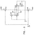
- FIGS. 3 and 4 show how to realize electronic switches with n-channel or p-channel MOS transistors by inserting symmetrically between two connection terminals SD and DS a pair of switching circuits of the type indicated in FIG. 1 or FIG. 2.
- transistors M11 and M21 and threshold transistors M11' and M21' are piloted by the same command signal.
- the transistors M13 and M23 and the transistors M13' and M23' are piloted.
Landscapes
- Metal-Oxide And Bipolar Metal-Oxide Semiconductor Integrated Circuits (AREA)
- Electronic Switches (AREA)
Priority Applications (3)
| Application Number | Priority Date | Filing Date | Title |
|---|---|---|---|
| EP95830122A EP0735682A1 (de) | 1995-03-31 | 1995-03-31 | MOS - Transistor - Schaltkreis ohne Körpereffekt |
| JP8074651A JPH08288814A (ja) | 1995-03-31 | 1996-03-28 | スイッチング回路 |
| US08/624,126 US5748029A (en) | 1995-03-31 | 1996-03-29 | MOS transistor switching circuit without body effect |
Applications Claiming Priority (1)
| Application Number | Priority Date | Filing Date | Title |
|---|---|---|---|
| EP95830122A EP0735682A1 (de) | 1995-03-31 | 1995-03-31 | MOS - Transistor - Schaltkreis ohne Körpereffekt |
Publications (1)
| Publication Number | Publication Date |
|---|---|
| EP0735682A1 true EP0735682A1 (de) | 1996-10-02 |
Family
ID=8221884
Family Applications (1)
| Application Number | Title | Priority Date | Filing Date |
|---|---|---|---|
| EP95830122A Withdrawn EP0735682A1 (de) | 1995-03-31 | 1995-03-31 | MOS - Transistor - Schaltkreis ohne Körpereffekt |
Country Status (3)
| Country | Link |
|---|---|
| US (1) | US5748029A (de) |
| EP (1) | EP0735682A1 (de) |
| JP (1) | JPH08288814A (de) |
Cited By (1)
| Publication number | Priority date | Publication date | Assignee | Title |
|---|---|---|---|---|
| CN119561529A (zh) * | 2025-01-24 | 2025-03-04 | 合肥市山海半导体技术有限公司 | 一种cmos开关电路 |
Families Citing this family (7)
| Publication number | Priority date | Publication date | Assignee | Title |
|---|---|---|---|---|
| JP3732914B2 (ja) * | 1997-02-28 | 2006-01-11 | 株式会社ルネサステクノロジ | 半導体装置 |
| US6239649B1 (en) * | 1999-04-20 | 2001-05-29 | International Business Machines Corporation | Switched body SOI (silicon on insulator) circuits and fabrication method therefor |
| US6744294B1 (en) * | 1999-05-12 | 2004-06-01 | Telefonaktiebolaget Lm Ericsson (Publ) | Cascode signal driver with low harmonic content |
| US6275094B1 (en) * | 1999-06-22 | 2001-08-14 | International Business Machines Corporation | CMOS device and circuit and method of operation dynamically controlling threshold voltage |
| US6326666B1 (en) | 2000-03-23 | 2001-12-04 | International Business Machines Corporation | DTCMOS circuit having improved speed |
| US7116151B2 (en) * | 2004-06-30 | 2006-10-03 | Intel Corporation | Stress tolerant high voltage back-to-back switch |
| US8143936B2 (en) * | 2008-09-12 | 2012-03-27 | Intel Mobile Communications GmbH | Application of control signal and forward body-bias signal to an active device |
Citations (5)
| Publication number | Priority date | Publication date | Assignee | Title |
|---|---|---|---|---|
| US3866064A (en) * | 1973-08-22 | 1975-02-11 | Harris Intertype Corp | Cmos analog switch |
| JPS63182907A (ja) * | 1987-01-26 | 1988-07-28 | Hitachi Ltd | スイツチト・キヤパシタ・フイルタ |
| JPH01276920A (ja) * | 1988-04-28 | 1989-11-07 | Ricoh Co Ltd | アナログ・スイッチ |
| EP0520470A2 (de) * | 1991-06-27 | 1992-12-30 | Fujitsu Limited | Ausgangsschaltung und Halbleiter integrierte Schaltung |
| US5191244A (en) * | 1991-09-16 | 1993-03-02 | Advanced Micro Devices, Inc. | N-channel pull-up transistor with reduced body effect |
-
1995
- 1995-03-31 EP EP95830122A patent/EP0735682A1/de not_active Withdrawn
-
1996
- 1996-03-28 JP JP8074651A patent/JPH08288814A/ja active Pending
- 1996-03-29 US US08/624,126 patent/US5748029A/en not_active Expired - Lifetime
Patent Citations (5)
| Publication number | Priority date | Publication date | Assignee | Title |
|---|---|---|---|---|
| US3866064A (en) * | 1973-08-22 | 1975-02-11 | Harris Intertype Corp | Cmos analog switch |
| JPS63182907A (ja) * | 1987-01-26 | 1988-07-28 | Hitachi Ltd | スイツチト・キヤパシタ・フイルタ |
| JPH01276920A (ja) * | 1988-04-28 | 1989-11-07 | Ricoh Co Ltd | アナログ・スイッチ |
| EP0520470A2 (de) * | 1991-06-27 | 1992-12-30 | Fujitsu Limited | Ausgangsschaltung und Halbleiter integrierte Schaltung |
| US5191244A (en) * | 1991-09-16 | 1993-03-02 | Advanced Micro Devices, Inc. | N-channel pull-up transistor with reduced body effect |
Non-Patent Citations (2)
| Title |
|---|
| PATENT ABSTRACTS OF JAPAN vol. 12, no. 457 (E - 688) 30 November 1988 (1988-11-30) * |
| PATENT ABSTRACTS OF JAPAN vol. 14, no. 51 (E - 881)<3994> 30 January 1990 (1990-01-30) * |
Cited By (1)
| Publication number | Priority date | Publication date | Assignee | Title |
|---|---|---|---|---|
| CN119561529A (zh) * | 2025-01-24 | 2025-03-04 | 合肥市山海半导体技术有限公司 | 一种cmos开关电路 |
Also Published As
| Publication number | Publication date |
|---|---|
| US5748029A (en) | 1998-05-05 |
| JPH08288814A (ja) | 1996-11-01 |
Similar Documents
| Publication | Publication Date | Title |
|---|---|---|
| US5617055A (en) | Electronic switch having reduced body effect | |
| US4857778A (en) | Programmable universal active filter | |
| EP0483419B1 (de) | Ganz differenzialer Abtast- und Haltkreisaddierer | |
| EP0158646B1 (de) | Schaltungen mit geschalteten kapazitäten | |
| US5748029A (en) | MOS transistor switching circuit without body effect | |
| EP0109642B1 (de) | Analogschalter | |
| JPH04313907A (ja) | 信号処理装置 | |
| JPH02188024A (ja) | レベルシフト回路 | |
| JPH04284021A (ja) | 出力回路 | |
| US5684425A (en) | Analog switch for low supply voltage MOS integrated circuits | |
| US6147541A (en) | Monolithic MOS-SC circuit | |
| JPH0413305A (ja) | 遅延回路 | |
| US4559498A (en) | Symmetrical integrator and application of said integrator to an electric filter | |
| JP3540401B2 (ja) | レベルシフト回路 | |
| US4644291A (en) | Operational amplifier | |
| US5847670A (en) | Offset voltage compensation for voltage comparators | |
| JPH0470212A (ja) | 複合論理回路 | |
| EP0821484A1 (de) | Hohen Spannungen widerstehende Ausgangsstufe | |
| US7573334B2 (en) | Bias control circuitry for amplifiers and related systems and methods of operation | |
| KR0154811B1 (ko) | 충분한 출력전압 변동폭을 주는 부트스트랩 인버터 | |
| JPS61192121A (ja) | アナログ信号のスイツチ回路 | |
| KR0130201B1 (ko) | N+ 주입 마스크(Implant Mask)를 이용한 출력선택 회로 | |
| JPS6057722A (ja) | GaAs疑似CMOSトランスフア−ゲ−ト | |
| JPH0458207B2 (de) | ||
| JPH037424A (ja) | トライステート回路 |
Legal Events
| Date | Code | Title | Description |
|---|---|---|---|
| PUAI | Public reference made under article 153(3) epc to a published international application that has entered the european phase |
Free format text: ORIGINAL CODE: 0009012 |
|
| AK | Designated contracting states |
Kind code of ref document: A1 Designated state(s): DE FR GB IT |
|
| 17P | Request for examination filed |
Effective date: 19970327 |
|
| RAP3 | Party data changed (applicant data changed or rights of an application transferred) |
Owner name: STMICROELECTRONICS S.R.L. |
|
| 17Q | First examination report despatched |
Effective date: 20010219 |
|
| STAA | Information on the status of an ep patent application or granted ep patent |
Free format text: STATUS: THE APPLICATION IS DEEMED TO BE WITHDRAWN |
|
| 18D | Application deemed to be withdrawn |
Effective date: 20010904 |