EP0735688A2 - Adiabatische Logik - Google Patents
Adiabatische Logik Download PDFInfo
- Publication number
- EP0735688A2 EP0735688A2 EP96302083A EP96302083A EP0735688A2 EP 0735688 A2 EP0735688 A2 EP 0735688A2 EP 96302083 A EP96302083 A EP 96302083A EP 96302083 A EP96302083 A EP 96302083A EP 0735688 A2 EP0735688 A2 EP 0735688A2
- Authority
- EP
- European Patent Office
- Prior art keywords
- signal
- output
- node
- input
- clock
- Prior art date
- Legal status (The legal status is an assumption and is not a legal conclusion. Google has not performed a legal analysis and makes no representation as to the accuracy of the status listed.)
- Withdrawn
Links
- 230000008859 change Effects 0.000 claims description 14
- 230000003068 static effect Effects 0.000 abstract description 6
- 230000007704 transition Effects 0.000 description 19
- 238000010586 diagram Methods 0.000 description 10
- 230000003111 delayed effect Effects 0.000 description 3
- 238000007599 discharging Methods 0.000 description 3
- 230000021715 photosynthesis, light harvesting Effects 0.000 description 3
- 230000004044 response Effects 0.000 description 3
- 150000001875 compounds Chemical group 0.000 description 2
- 230000008901 benefit Effects 0.000 description 1
- 230000002427 irreversible effect Effects 0.000 description 1
- 238000000034 method Methods 0.000 description 1
- 230000003252 repetitive effect Effects 0.000 description 1
Images


Classifications
-
- H—ELECTRICITY
- H03—ELECTRONIC CIRCUITRY
- H03K—PULSE TECHNIQUE
- H03K19/00—Logic circuits, i.e. having at least two inputs acting on one output; Inverting circuits
-
- H—ELECTRICITY
- H03—ELECTRONIC CIRCUITRY
- H03K—PULSE TECHNIQUE
- H03K19/00—Logic circuits, i.e. having at least two inputs acting on one output; Inverting circuits
- H03K19/0008—Arrangements for reducing power consumption
- H03K19/0019—Arrangements for reducing power consumption by energy recovery or adiabatic operation
Definitions
- This invention relates to logic circuitry. More specifically, this invention relates to logic circuitry having low power consumption and simplified topology.
- nodes are charged and discharged in a completely irreversible, dissipative manner, using a switch to charge a node to a first potential and to discharge the node to a second potential. It has been proposed to attach such a node to a slew rate limited clock which in theory gradually, adiabatically, and reversibly charges and discharges the node.
- Logic circuitry using this technique is currently too complicated and uses too many transistors so that, at normal speeds of operation, any power savings for each transistor may be lost by the fact that many more transistors are used to accomplish simple logical operations.
- an electronic circuit in accordance with one example of the invention, includes an input node and an output node.
- the input node carries signals varying between two potentials in an adiabatic fashion without substantial dissipative energy losses.
- the output node carries corresponding output signals varying between two potentials in a similar adiabatic fashion.
- the nature of the signals carried by the input and output nodes is such that they may signify at least two possible logical states or levels.
- the electronic circuit in accordance with this example of the invention also has a clock node which may be connected to an energy source which produces at least one clock signal varying between two potentials in an adiabatic fashion.
- the electronic circuit also contains a means for selectively permitting current flow between the clock node and the output node to selectively charge the output node during predetermined portions of the clock signal in response to the state of the input signal.
- This means also selectively prevents current flow between the output node and the clock node to selectively prevent discharge of the output node in response to the state of the input signal.
- the input signal may be prevented from making transitions between potentials at certain times in the cycle of the clock signal to enhance the adiabatic nature of the electronic circuit.
- Adiabatic computing using logic circuitry in accordance with this invention is expected to have a great impact on a wide range of applications from battery powered products to high performance systems where power dissipation is an important consideration.
- FIG. 1 is a schematic diagram of an example of an adiabatic inverter in accordance with this invention.
- FIG. 2 is a timing diagram showing the input, the output, and the clock voltages associated with the inverter of FIG. 1.
- FIG. 3 is a schematic diagram of an adiabatic NAND gate in accordance with this invention.
- FIG. 4 is a schematic diagram of an adiabatic NOR gate in accordance with this invention.
- FIG. 5 is a schematic diagram of an adiabatic NAND/NOR gate in accordance with this invention.
- FIG. 6 is a schematic diagram of a multiple stage adiabatic logic circuit in accordance with this invention.
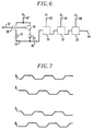
- FIG. 7 is a timing diagram showing the clock voltages for the multiple stage logic circuit shown in FIG. 6.
- FIG. 8 is a schematic diagram of a storage element in accordance with this invention.
- FIG. 9 is a schematic diagram of a non-inverter in accordance with this invention.
- FIG. 1 shows one example of a logic gate in accordance with this invention.
- the gate shown in FIG. 1 is an inverter and comprises a logic element in the form of two controllable switches, which FIG. 1 shows as an n-channel FET 10 and a p-channel FET 11 normally used in conventional CMOS circuitry.
- the inverter of FIG. 1 has an input node 12, an output node 13, and a clock node 14.
- the gates or control terminals of the FETs 10 and 11 are connected to the input node 12.
- the clock node 14 of the FIG. 1 circuit is connected to a clock signal generator 15 which produces a clock signal, the waveform of which is represented by the top waveform in FIG. 2.
- the input node is connected to a signal source which produces an input signal which may have one of two potentials representing two possible input logic levels. Transitions between input logic levels may involve transitions between the two predetermined potential levels. As shown in FIG. 2, the input signal may make transitions between the two logic levels adiabatically, namely, at a reduced voltage rate of change which minimizes energy dissipation in the circuit of FIG. 1.
- a signal or a node in this invention makes an adiabatic transition from one state to another state when the energy dissipated in the apparatus which causes the transition is substantially smaller than the energy difference between the two states.
- the energy difference between one logic level and another logic level is 1/2 CV 2 , where C is the effective capacitance associated with a node and V is the voltage or potential change taking place as a result of the node making a transition from one logic level to another logic level
- the transition from one logic level to another is adiabatic if substantially less than 1/2 CV 2 , such as 1/4 CV 2 to as low as 1/20 CV 2 or less, is dissipated in connection with making the transition.
- each of the FETs 10 and 11 is connected to the clock node 14 which is connected to the clock signal source 15 described above.
- the clock signal from the source 15 varies between two states or potential levels.
- the clock signal variations occur at an adiabatic reduced rate of change to minimize energy dissipation in the circuit of FIG. 1.
- the output node 13 carries an output signal which has one of two possible output logic levels. Like the input signal and the clock signal, transitions of the output signal between logic levels involves transitions between two predetermined potentials. Transitions between output logic levels occur in a nondissipative adiabatic fashion similar to that occurring in connection with transitions of the input signal and the clock signal.
- a diode 16 is connected between the other of the output terminals of the FET 10 and the output node 13 as shown in FIG. 1.
- Another diode 17 is connected between the other output terminal of the transistor 11 and the output node 13.
- FIG. 1 shows the controllable switches 10 and 11 as being FETs, any controllable switch, such as bipolar transistors, may be used in a corresponding circuit configuration to achieve the function of an inverter in accordance with this invention.
- FIG. 2 is a timing diagram illustrating the operation of the logic gate of FIG. 1.
- a signal appearing at the input terminal of the logic gate is at a high level, which can be a substantially constant voltage level or potential of a predetermined magnitude.
- the signal appearing at the output terminal of the logic gate is at a low level, which can be another substantially constant voltage level or potential of a predetermined magnitude.
- the signal appearing at the output terminal is at a high level.
- the output signal follows the next trailing edge 19 of the clock signal downwardly to a low level, as shown at reference numeral 20.
- the output signal remains at a constant (static) low level as long as the input signal is high, regardless of further variation in the clock signal level. If the input signal goes from high to low, as shown at reference numeral 21, then the output signal follows the clock upwardly as shown at reference numeral 23 to a high level on the next leading edge 22 of the clock pulses. The output signal remains at a constant (static) high level as long as the input signal continues to be low, regardless of further variation in the clock signal level.
- FIG. 2 illustrates the nature of the adiabatic clocking signal applied to the logic gate of FIG. 1.
- the clocking signal is a repetitive signal having a predetermined period T.
- the clocking signal begins at a low level and increases gradually to a high level during a period labeled A in FIG. 2.
- the clock then remains at a high level for a certain period of time labeled B in FIG. 2.
- This period of time can be any predetermined amount of time, even zero.
- the clock signal then gradually returns to a low level during a period labeled C in FIG. 2.
- the clock signal remains at a low level during a predetermined time period labeled D in FIG. 2, after which the previously described cycle is repeated.
- a trapezoidally shaped clock signal is shown here, it could be just as easily a similarly shaped waveform such as a sinusoidal waveform.
- An advantage of a sinusoidal waveform is that it may easily be produced by conventional LC oscillator circuitry.
- a logic circuit such as the one shown in FIG. 1 may be approximated by simple series resistance-capacitance (RC) circuits in analyzing its response to switching signals such as the input logic signal and the clock signal shown specifically in FIG. 2.
- RC resistance-capacitance
- the slope of the signals in the circuit of FIG. 1, such as the input signal and the clock signal, is reduced such that the circuit of FIG. 1 operates in an adiabatic fashion.
- the slopes are gradual enough so that capacitances associated with the circuit of FIG. 1 are able to charge and discharge in substantial conformance with the changing voltage signals.
- the time for the clock or other changing signal to reach a high state from a low state, or vice versa, (“the ramp time") may be greater than the time constant of the previously mentioned RC circuit.
- the ramp time may be at least ten times the time constant. This will mean that there are minimal voltages appearing across resistances found in the charging and discharging paths connected to the changing signal. This also will mean that there is minimal energy dissipation during the charging and discharging created by the operation of the changing signal. This will ensure that state transitions on the input and output nodes of the circuit of FIG. 1 will be adiabatic, namely, the energy irretrievably dissipated in the apparatus will be substantially less than the energy difference between the two states.
- the input signals are substantially prevented from making sudden transitions from one state to another. They may also be prevented from making any state changes during predetermined portions of the clock signal of FIG. 1.
- the input signals may be constrained to make transitions from one logic state or level to another logic state or level only when the clock signal is low (period D, for example) in the case of input transitions from high to low and only when the clock signal is high (period B, for example) in the case of input transitions from low to high.
- the signals in circuits in accordance with this invention are only allowed to change from one potential to another such that a switch does not close when there is substantial voltage across the switch and a switch does not open when there is substantial current is flowing through it. If this rule is followed, then in some instances it is not required to greatly limit the rate of change of certain signals to preserve the adiabatic nature of the operation of that circuitry. For example, if the input signals to controlled switches, such as the FETs 10 and 11 in FIG. 1, are constrained to change state only when there is no voltage across the output terminals of those controlled switches, then there does not have to be a great deal of restriction on the rate of change of those input signals for adiabatic operation to be obtained.
- FIG. 3 illustrates a representative NAND gate constructed in accordance with the principles of this invention.
- the NAND gate comprises two series connected controllable switches in the form of n-channel FETs 24 and 25 connected in series with a diode 26 between a clock node 26 and an output node 27.
- the circuit of FIG. 3 also includes a parallel connected combination of two p-channel FETs 27 and 28.
- the parallel combination of FETs 27 and 28 are connected in series with a diode 29 between the clock node 26 and the output node 27.
- the clock node 26 is connected to a source 15, as described above.
- Gates capable of performing the NAND operation for more than two input signals A and B may be constructed by providing additional controllable switches. Each input involved in the NAND operation is directed to a respective input node and corresponding control terminal of each of the controllable switches.
- the NAND gate of FIG. 4 is shown to involve FETs, other kinds of controllable switches may be used, including NPN and PNP bipolar transistors and the like.
- FIG. 4 shows a representative NOR gate constructed in accordance with the principles of this invention.
- the NOR gate of FIG. 5 comprises a pair of parallel connected controllable switches, such as a pair of n-channel FETs 33 and 34, connected in series with a diode 35. This combination of the switches and the diode is connected between a clock node 36 and an output node 37.
- a series combination of a p-channel FET 40, a p-channel FET 41, and a diode 42 also is connected between the clock node 36 and the output node 37.
- a clock signal similar to the clock signals in the circuitry of FIGS. 1 and 3, is directed to the clock 36 node in FIG. 4.
- the circuit of FIG. 5 comprises a pair of parallel connected controllable switches, such as a pair of n-channel FETs 33 and 34, connected in series with a diode 35. This combination of the switches and the diode is connected between a clock node 36 and an output node 37.
- NOR gate 4 produces an output signal at node 37 which is a logical NOR of the two input signals A and B directed to respective input nodes 38 and 39 of the NOR gate in FIG. 4.
- the NOR gate of FIG. 4 uses FETs as switching devices, NOR gates using other kinds of controllable switches may be used in place of the FETs 33, 34, 40, and 41, including NPN and PNP bipolar transistors and the like.
- FIG. 5 illustrates an adiabatic logic circuit in accordance with this invention which performs compound logical operations on a set of input signals A, B, and C.
- the circuit of FIG. 5 comprises two series connected n-channel FETs 43 and 44 in parallel with an n-channel FET 45.
- a diode 46 is connected in series with this combination of three FETs.
- the three FETs 43-45 and the diode 40 are connected between a clock node 47 and an output node 48.
- the circuit of FIG. 5 includes two parallel connected p-channel FETs 49 and 50 in series with a p-channel FET 51.
- the three FETs 49-51 are connected in series with a diode 52 between the clock node 47 and the output node 48.
- a clock signal is directed to the clock node 47.
- the clock signal is similar to the clock signals directed to the clock nodes of the other logic circuits described above.
- the circuit of FIG. 5 produces an output signal at output node 48 which is the logical function A ⁇ B+C ⁇ of the input signals A, B, and C applied to input nodes of the FIG. 5 device.
- Other controllable switches may be used in place of the FETs shown in FIG. 5.
- FIG. 6 shows an example of a logic circuit using previously described adiabatic logic building blocks.
- the circuit of FIG. 6 comprises four inverter stages 53, 54, 55, and 56 in series functioning as a shift register.
- Stage 53 is shown in detail in FIG. 6 and is an inverter similar to the inverter shown in FIG. 1. It comprises an input node 57 connected to the control terminal of an n-channel FET 58 and a p-channel FET 59.
- a diode 61 connects one output terminal of the FET 58 to an output node 60 of the inverter 53.
- Another output terminal of the FET 58 is connected to a clock node 62.
- the clock node 62 is connected to an energy source producing a clock signal ⁇ 0 similar to the clock signal in the circuit of FIG. 1. This clock signal is depicted as the topmost waveform ⁇ 0 shown in FIG. 7.
- a diode 63 connects one output terminal of the FET 59 to the output node 60. The other output terminal of FET 59 is connected to the clock node 62.
- Each of the inverters 54, 55, and 56 is identical to the inverter 53.
- the output node 60 of the inverter 53 is connected to the input node of the inverter 54.
- the output node of the inverter 54 is connected to the input node of the inverter 55, the output node of the inverter 55 is connected to the input node of the inverter 56, and the output node of the inverter 56 is connected to an output 64 of the shift register of FIG. 6.
- a clock node 65 is connected to the output terminals of the FETs in the inverter 54 and receives a clock signal ⁇ 1 produced by an energy source.
- the clock signal ⁇ 1 is similar to the clock signal ⁇ 0 for the inverter 53 shown in FIG. 7 and is specifically shown in FIG. 7 as the waveform second from the top labeled ⁇ 1 .
- the clock signal ⁇ 1 in this example of the invention is delayed by three quarters of a clock cycle with respect to the clock signal ⁇ 0 .
- a clock signal ⁇ 2 shown in FIG. 7 is directed to the clock node 66 of the inverter 55.
- the clock signal ⁇ 2 is delayed by three quarters of a clock cycle with respect to the clock signal ⁇ 1 .
- the clock signal ⁇ 2 thus is the inverse of the clock signal ⁇ 0 ).
- a clock signal ⁇ 3 is directed to the clock node 68 of the inverter 56. The details of the clock signal ⁇ 3 are shown as the bottom most waveform in FIG. 7. The clock signal ⁇ 3 is delayed by three quarters of a clock cycle with respect to the clock signal ⁇ 2 . Although FIG. 7 shows that they are not connected, it should be pointed out that the output 64 can be safely connected to the input node 57 of the inverter 53.
- FIG. 8 shows a storage element in accordance with this invention.
- the storage element comprises two inverters like the one shown in FIG. 1.
- the inverters are,both connected to a common clock signal produced by a clock signal generator like the clock signal generator 15 shown in FIG. 1.
- the output node of the inverter comprising n-channel FET Q1, p-channel FET Q2, diode D1, and diode D2 is connected to the input node of the inverter comprising n-channel FET Q3, p-channel FET Q4, diode D3, and diode D4.
- the output node of the Q3, Q4, D3, D4 inverter is fed back to the input node of the Q1, Q2, D1, D2 inverter.
- FIG. 9 The noninverter of FIG. 9 comprises two series connected inverters 69 and 70, each of which is the same as the inverter shown in FIGs 1 and 2. Both inverters 69 and 70 are connected to a common clock, which is the same as the clock signal generator 15 in FIGs 1 and 2. The output of the inverter 70 is a non-inverted version of the input to the inverter 69.
- the logic circuitry is simple and has vastly reduced power dissipation.
Landscapes
- Physics & Mathematics (AREA)
- Engineering & Computer Science (AREA)
- Computer Hardware Design (AREA)
- Computing Systems (AREA)
- General Engineering & Computer Science (AREA)
- Mathematical Physics (AREA)
- Logic Circuits (AREA)
Applications Claiming Priority (2)
| Application Number | Priority Date | Filing Date | Title |
|---|---|---|---|
| US08/413,658 US5521538A (en) | 1995-03-30 | 1995-03-30 | Adiabatic logic |
| US413658 | 1995-03-30 |
Publications (1)
| Publication Number | Publication Date |
|---|---|
| EP0735688A2 true EP0735688A2 (de) | 1996-10-02 |
Family
ID=23638109
Family Applications (1)
| Application Number | Title | Priority Date | Filing Date |
|---|---|---|---|
| EP96302083A Withdrawn EP0735688A2 (de) | 1995-03-30 | 1996-03-26 | Adiabatische Logik |
Country Status (9)
| Country | Link |
|---|---|
| US (1) | US5521538A (de) |
| EP (1) | EP0735688A2 (de) |
| JP (1) | JPH08335873A (de) |
| KR (1) | KR960036332A (de) |
| CA (1) | CA2172096A1 (de) |
| IL (1) | IL117641A0 (de) |
| MX (1) | MX9601147A (de) |
| SG (1) | SG83641A1 (de) |
| TW (1) | TW297187B (de) |
Cited By (1)
| Publication number | Priority date | Publication date | Assignee | Title |
|---|---|---|---|---|
| DE10101951A1 (de) * | 2001-01-17 | 2002-08-01 | Infineon Technologies Ag | Transistor-Dioden-Anordnung |
Families Citing this family (20)
| Publication number | Priority date | Publication date | Assignee | Title |
|---|---|---|---|---|
| USRE38918E1 (en) | 1994-04-22 | 2005-12-13 | University Of Southern California | System and method for power-efficient charging and discharging of a capacitive load from a single source |
| US5473526A (en) | 1994-04-22 | 1995-12-05 | University Of Southern California | System and method for power-efficient charging and discharging of a capacitive load from a single source |
| JPH08148982A (ja) * | 1994-11-21 | 1996-06-07 | Yamaha Corp | 半導体集積回路 |
| US5670899A (en) * | 1994-11-21 | 1997-09-23 | Yamaha Corporation | Logic circuit controlled by a plurality of clock signals |
| US5602497A (en) * | 1995-12-20 | 1997-02-11 | Thomas; Steven D. | Precharged adiabatic pipelined logic |
| US5841299A (en) * | 1997-02-06 | 1998-11-24 | Intel Corporation | Method and apparatus for implementing an adiabatic logic family |
| US5986476A (en) * | 1997-08-08 | 1999-11-16 | Intel Corporation | Method and apparatus for implementing a dynamic adiabatic logic family |
| US6242951B1 (en) * | 1997-09-05 | 2001-06-05 | Shunji Nakata | Adiabatic charging logic circuit |
| US6985142B1 (en) * | 1998-09-03 | 2006-01-10 | University Of Southern California | Power-efficient, pulsed driving of capacitive loads to controllable voltage levels |
| FR2796224B1 (fr) | 1999-07-08 | 2001-09-07 | Suisse Electronique Microtech | Circuit logique adiabatique |
| US7005893B1 (en) * | 1999-07-19 | 2006-02-28 | University Of Southern California | High-performance clock-powered logic |
| US6415181B1 (en) * | 2000-02-25 | 2002-07-02 | Medtronic, Inc. | Implantable medical device incorporating adiabatic clock-powered logic |
| US6433389B1 (en) | 2000-06-09 | 2002-08-13 | Advanced Micro Devices, Inc. | Silicon on insulator logic circuit utilizing diode switching elements |
| EP1303881A1 (de) * | 2000-06-02 | 2003-04-23 | Advanced Micro Devices, Inc. | Diodenschaltelemente verwendender silizium-auf-isolator logikschaltkreis |
| JP3632151B2 (ja) | 2000-06-06 | 2005-03-23 | 日本電信電話株式会社 | 断熱充電レジスタ回路 |
| CN101087128B (zh) * | 2006-06-07 | 2010-08-25 | 黑龙江大学 | 绝热锁存器和无绝热门的绝热cmos时序电路 |
| JP5239501B2 (ja) * | 2008-05-15 | 2013-07-17 | セイコーエプソン株式会社 | 2相駆動cmos断熱的論理回路 |
| TWI539749B (zh) | 2015-03-31 | 2016-06-21 | 國立交通大學 | 能量回收系統及其回收方法 |
| KR101722558B1 (ko) * | 2015-08-28 | 2017-04-04 | 서울과학기술대학교 산학협력단 | 단일 다이오드를 사용한 adcl 인버터 |
| US10817463B1 (en) * | 2019-09-30 | 2020-10-27 | Zettaflops Llc | Adiabatic circuits for cold scalable electronics |
Family Cites Families (9)
| Publication number | Priority date | Publication date | Assignee | Title |
|---|---|---|---|---|
| US3651340A (en) * | 1970-06-22 | 1972-03-21 | Hamilton Watch Co | Current limiting complementary symmetry mos inverters |
| US4142251A (en) * | 1977-11-21 | 1979-02-27 | Hewlett-Packard Company | Field programmable read-only-memory |
| US4985643A (en) * | 1988-06-24 | 1991-01-15 | National Semiconductor Corporation | Speed enhancement technique for CMOS circuits |
| US5121003A (en) * | 1990-10-10 | 1992-06-09 | Hal Computer Systems, Inc. | Zero overhead self-timed iterative logic |
| US5208490A (en) * | 1991-04-12 | 1993-05-04 | Hewlett-Packard Company | Functionally complete family of self-timed dynamic logic circuits |
| WO1994002993A1 (en) * | 1992-07-17 | 1994-02-03 | Massachusetts Institute Of Technology | Recovered energy logic circuits |
| US5378940A (en) * | 1993-03-12 | 1995-01-03 | Massachusetts Institute Of Technology | Charge recovery logic including split level logic |
| US5422582A (en) * | 1993-12-30 | 1995-06-06 | At&T Corp. | Diode coupled CMOS logic design for quasi-static resistive dissipation with multi-output capability |
| US5426382A (en) * | 1994-05-03 | 1995-06-20 | Motorola, Inc. | Complementary logic recovered energy circuit |
-
1995
- 1995-03-30 US US08/413,658 patent/US5521538A/en not_active Expired - Lifetime
- 1995-12-04 TW TW084112889A patent/TW297187B/zh active
-
1996
- 1996-03-19 CA CA002172096A patent/CA2172096A1/en not_active Abandoned
- 1996-03-25 IL IL11764196A patent/IL117641A0/xx unknown
- 1996-03-26 EP EP96302083A patent/EP0735688A2/de not_active Withdrawn
- 1996-03-27 MX MX9601147A patent/MX9601147A/es not_active Application Discontinuation
- 1996-03-29 JP JP8075510A patent/JPH08335873A/ja not_active Withdrawn
- 1996-03-29 SG SG9606300A patent/SG83641A1/en unknown
- 1996-03-30 KR KR1019960009654A patent/KR960036332A/ko not_active Withdrawn
Cited By (1)
| Publication number | Priority date | Publication date | Assignee | Title |
|---|---|---|---|---|
| DE10101951A1 (de) * | 2001-01-17 | 2002-08-01 | Infineon Technologies Ag | Transistor-Dioden-Anordnung |
Also Published As
| Publication number | Publication date |
|---|---|
| MX9601147A (es) | 1997-02-28 |
| CA2172096A1 (en) | 1996-10-01 |
| TW297187B (de) | 1997-02-01 |
| IL117641A0 (en) | 1996-07-23 |
| SG83641A1 (en) | 2001-10-16 |
| KR960036332A (ko) | 1996-10-28 |
| JPH08335873A (ja) | 1996-12-17 |
| US5521538A (en) | 1996-05-28 |
Similar Documents
| Publication | Publication Date | Title |
|---|---|---|
| US5521538A (en) | Adiabatic logic | |
| Seitz et al. | Hot clock nMOS | |
| US7385440B2 (en) | Bootstrapped switch for sampling inputs with a signal range greater than supply voltage | |
| US5323066A (en) | Method and apparatus for performing power on reset initialization in a data processing system | |
| US4849661A (en) | CMOS input buffer with switched capacitor reference voltage generator | |
| US5473269A (en) | Adiabatic dynamic logic | |
| US5155379A (en) | Clocked driver circuit stabilized against changes due to fluctuations in r.c. time constant | |
| US5473270A (en) | Adiabatic dynamic precharge boost circuitry | |
| US5517145A (en) | CMOS toggle flip-flop using adiabatic switching | |
| JPH05276016A (ja) | ランダム論理適用のための動的レイショレス・サーキットリー | |
| WO2014138033A1 (en) | Voltage level shifter with a low-latency voltage boost circuit | |
| US5602497A (en) | Precharged adiabatic pipelined logic | |
| US5477164A (en) | Adiabatic dynamic noninverting circuitry | |
| US4472645A (en) | Clock circuit for generating non-overlapping pulses | |
| US5999019A (en) | Fast CMOS logic circuit with critical voltage transition logic | |
| US5422582A (en) | Diode coupled CMOS logic design for quasi-static resistive dissipation with multi-output capability | |
| Takahashi et al. | Two-phase clocked CMOS adiabatic logic | |
| JPH06224730A (ja) | 出力バッファ回路 | |
| US5426382A (en) | Complementary logic recovered energy circuit | |
| US6943589B2 (en) | Combination multiplexer and tristate driver circuit | |
| EP0743648A1 (de) | Ausgabestufe für integrierte Schaltungen, insbesondere für elektronische Speicher | |
| KR100299050B1 (ko) | 상보 게이트-소스 클럭구동회로와 이를 적용한 플립플롭 | |
| JP2574839B2 (ja) | クロック駆動回路 | |
| JPH06187785A (ja) | Atd回路 | |
| JPS63119323A (ja) | 絶縁ゲ−ト型出力バツフア回路 |
Legal Events
| Date | Code | Title | Description |
|---|---|---|---|
| PUAI | Public reference made under article 153(3) epc to a published international application that has entered the european phase |
Free format text: ORIGINAL CODE: 0009012 |
|
| AK | Designated contracting states |
Kind code of ref document: A2 Designated state(s): DE ES FR GB IT NL SE |
|
| STAA | Information on the status of an ep patent application or granted ep patent |
Free format text: STATUS: THE APPLICATION HAS BEEN WITHDRAWN |
|
| 18W | Application withdrawn |
Withdrawal date: 19971127 |