EP0736907B1 - Feldeffekt steuerbares Halbleiterbauelement mit einem integrierten ohmischen Widerstand - Google Patents
Feldeffekt steuerbares Halbleiterbauelement mit einem integrierten ohmischen Widerstand Download PDFInfo
- Publication number
- EP0736907B1 EP0736907B1 EP96104243A EP96104243A EP0736907B1 EP 0736907 B1 EP0736907 B1 EP 0736907B1 EP 96104243 A EP96104243 A EP 96104243A EP 96104243 A EP96104243 A EP 96104243A EP 0736907 B1 EP0736907 B1 EP 0736907B1
- Authority
- EP
- European Patent Office
- Prior art keywords
- contact area
- gate electrode
- gate
- reactive resistor
- contact
- Prior art date
- Legal status (The legal status is an assumption and is not a legal conclusion. Google has not performed a legal analysis and makes no representation as to the accuracy of the status listed.)
- Expired - Lifetime
Links
Images

Classifications
-
- H—ELECTRICITY
- H10—SEMICONDUCTOR DEVICES; ELECTRIC SOLID-STATE DEVICES NOT OTHERWISE PROVIDED FOR
- H10D—INORGANIC ELECTRIC SEMICONDUCTOR DEVICES
- H10D48/00—Individual devices not covered by groups H10D1/00 - H10D44/00
- H10D48/30—Devices controlled by electric currents or voltages
- H10D48/32—Devices controlled by only the electric current supplied, or only the electric potential applied, to an electrode which does not carry the current to be rectified, amplified or switched
- H10D48/36—Unipolar devices
-
- H—ELECTRICITY
- H10—SEMICONDUCTOR DEVICES; ELECTRIC SOLID-STATE DEVICES NOT OTHERWISE PROVIDED FOR
- H10D—INORGANIC ELECTRIC SEMICONDUCTOR DEVICES
- H10D64/00—Electrodes of devices having potential barriers
- H10D64/20—Electrodes characterised by their shapes, relative sizes or dispositions
- H10D64/27—Electrodes not carrying the current to be rectified, amplified, oscillated or switched, e.g. gates
- H10D64/311—Gate electrodes for field-effect devices
- H10D64/411—Gate electrodes for field-effect devices for FETs
- H10D64/511—Gate electrodes for field-effect devices for FETs for IGFETs
- H10D64/517—Gate electrodes for field-effect devices for FETs for IGFETs characterised by the conducting layers
- H10D64/519—Gate electrodes for field-effect devices for FETs for IGFETs characterised by the conducting layers characterised by their top-view geometrical layouts
-
- H—ELECTRICITY
- H10—SEMICONDUCTOR DEVICES; ELECTRIC SOLID-STATE DEVICES NOT OTHERWISE PROVIDED FOR
- H10D—INORGANIC ELECTRIC SEMICONDUCTOR DEVICES
- H10D64/00—Electrodes of devices having potential barriers
- H10D64/60—Electrodes characterised by their materials
- H10D64/605—Source, drain, or gate electrodes for FETs comprising highly resistive materials
-
- H—ELECTRICITY
- H10—SEMICONDUCTOR DEVICES; ELECTRIC SOLID-STATE DEVICES NOT OTHERWISE PROVIDED FOR
- H10W—GENERIC PACKAGES, INTERCONNECTIONS, CONNECTORS OR OTHER CONSTRUCTIONAL DETAILS OF DEVICES COVERED BY CLASS H10
- H10W72/00—Interconnections or connectors in packages
- H10W72/50—Bond wires
- H10W72/531—Shapes of wire connectors
- H10W72/5363—Shapes of wire connectors the connected ends being wedge-shaped
Definitions
- the invention relates to a controllable by field effect Semiconductor component with a semiconductor body on which one isolated from the surface of the semiconductor body doped polysilicon layer is arranged, one of which first part is a gate electrode and a second part is one Contact area for a gate lead.
- Semiconductor components of the aforementioned that can be controlled by field effect Type e.g. Power MOSFET or IGBT are state of the art Technology. E.g. there are generally many such in modules Semiconductor components connected in parallel. Because of of the parasitic line inductances in the control circuit tend such arrangements when leading control to vibrations that prevent a defined switching on.
- a power MOS transistor is described in US Pat. No. 4,920,388. which contains a polycrystalline silicon layer, the as a resistance between a gate metallization and the gate terminal of the power MOS transistor is used. Furthermore, the semiconductor component contains a second one Area of a gate metallization that is adjacent to the active The source gate region of the component lies.
- JP-A-05055588 is a multi-chip-like MOS field effect transistor described a resistance with a higher Has impedance as a bond wire, and that between the Gate electrode and the gate contact area lies.
- the resistance is in by a lightly doped polysilicon layer a predetermined area.
- JP-A-62098670 is a semiconductor device with one with the gate connected in series resistance, arranged between the gate pad and the gate is.
- the resistor is made of polysilicon and its resistance value can be adjusted by ion implantation.
- the invention has for its object a field effect controllable semiconductor device of the type described to develop such that a simple and inexpensive Manufacturability is possible. Furthermore, the contact area easy and safe to contact for a gate lead be.
- the contact surface on Edge is provided with at least one recess, the ohmic resistance is arranged in the recess.
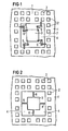
- Figure 1 is a section of a controllable by field effect Semiconductor device shown.
- the surface of a semiconductor body is covered with an insulating layer (not shown), on which in turn a doped polysilicon layer is arranged.
- the polysilicon layer has one first part 1, which serves as a gate electrode and a second Part 3, which is the contact surface for attaching a Gate lead forms.
- the gate electrode 1 of the polysilicon layer is provided with openings 2 through which -insulated against the polysilicon layer - via contact holes Source zones of the individual cells of the semiconductor component are contacted. These contact holes form a regular, distributed over the surface of the gate electrode 1 Template. To accommodate so-called gate contact fingers better distribution of the gate potential with larger chips can open wider areas 7 between adjacent cells of contact holes.
- the gate electrode 1 has a recess 4 in which the contact area 3 is arranged. Between the contact surface 3 and the gate electrode 1 is the doped polysilicon e.g. by Etching interrupted. In the recess 4 are between the Contact surface 3 and the gate electrode 1 islands 5, the integrated form ohmic resistors. They preferably exist made of doped polycrystalline silicon and have the same Doping like the contact area 3 and the gate electrode 1. They preferably also have the same thickness as 1 and 3.
- the islands 5 are on the one hand via conductor tracks 6 with the Gate electrode 1 and on the other hand with the contact surface 3 connected.
- the islands 5 can be generated simultaneously with the structuring of the contact area 3 and the gate electrode 1. Their length and cross-section depend on the size of the gate series resistor R g .
- the contact surface 3 is connected to the gate electrode 1 by means of webs 8.
- webs 8. are. These also consist of polysilicon. Their length and their cross section in turn depend on the resistance value that the gate series resistor R g should have.
- the embodiment of Figure 3 differs from that of Figure 1 in that the islands 5 in recesses 24th a contact surface 23 are arranged.
- the islands become 5 here as in the embodiment of Figure 1 by conductor tracks on the one hand with the contact surface 23 and on the other hand with contacted the gate electrode 1.
- the recesses 24 can as shown at the corners of the contact surface 23 or also in other places of the scope.
- the islands 5 can like the cutouts are square, other shapes are possible.
- Figure 4 it is shown that the surface of a semiconductor device with the semiconductor zones 11, 14 with a Oxide layer 12 is covered. This lies on the oxide layer 12 structured polysilicon layer consisting of the contact area 3, the islands 5 and the gate electrode 1.
- On the Polysilicon layer is an insulating layer 10 that both the gate electrode 1 and the contact surface 3 and Islands 5 covered.
- On the oxide layer 10 is above the Contact surface 3, a metal layer 14 is arranged.
- On the Gate electrode 1 sits a mentioned in connection with Figure 1 Gate contact finger 15. It is also through a metal layer educated.
- the metal layer 14 is on the contact surface 3 via contact holes 19 with the underlying polysilicon layer electrically connected. In the same way it is Gate contact finger 15 via contact holes 16 with the gate electrode 1 connected.
- the separate conductor tracks 6 are via contact holes 17 with the island's 5 polysilicon, which is the resistor represents connected.
- the metal layer 14 protrudes a bond wire 18 with an external connection of the semiconductor component in connection.
- the islands 5 or the webs 8 are according to one Embodiment by 0.5 to 1 micron thick polysilicon educated. Their width and length can e.g. 0.5 mm be.
- the polysilicon can e.g. be endowed in such a way that it has a resistance of 20 ohms / ⁇ .
Landscapes
- Semiconductor Integrated Circuits (AREA)
- Insulated Gate Type Field-Effect Transistor (AREA)
- Electrodes Of Semiconductors (AREA)
Description
- Figuren 1 bis 3
- die Aufsicht auf je ein Ausführungsbeispiel und
- Figur 4
- einen Schnitt durch ein weiteres Ausführungsbeispiel.
Claims (5)
- Durch Feldeffekt steuerbares Halbleiterbauelement mit einem Halbleiterkörper, auf dem eine gegen die Oberfläche des Halbleiterkörpers isolierte dotierte Polysiliziumschicht angeordnet ist, von der ein erster Teil eine Gateelektrode (1) ist und ein zweiter Teil eine Kontaktfläche (3) für eine Gatezuleitung, worin die Kontaktfläche mit der Gateelektrode über mindestens einen zwischen der Kontaktfläche (3) und Gateelektrode (1) liegenden integrierten ohmschen Widerstand elektrisch verbunden ist, wobei der ohmsche Widerstand aus dotiertem polykristallinem Silizium besteht,
dadurch gekennzeichnet, daß die Kontaktfläche (23) am Rand mit mindestens einer Aussparung (24) versehen ist und daß der ohmsche Widerstand (5) in der Aussparung angeordnet ist. - Halbleiterbauelement nach Anspruch 1,
dadurch gekennzeichnet, daß der ohmsche Widerstand über mindestens eine Leiterbahn (6) mit der Kontaktfläche (3) und über mindestens eine Leiterbahn (6) mit der Gateelektrode (1) verbunden ist. - Halbleiterbauelement nach Anspruch 1,
dadurch gekennzeichnet, daß die Kontaktfläche (3) rechteckig ausgebildet ist und daß an oder in der Nähe jeder Ecke ein ohmscher Widerstand (5) angeordnet ist. - Halbleiterbauelement nach Anspruch 3,
daß jede Ecke der Kontaktfläche eine quadratische Aussparung (24) hat und daß in jeder Aussparung ein quadratisch ausgebildeter ohmscher Widerstand (5) angeordnet ist. - Halbleiterbauelement nach Anspruch 1 oder 2,
dadurch gekennzeichnet, daß die Kontaktfläche (3), der ohmsche Widerstand (5) und die Gateelektrode (1) mit einer Isolierschicht (10) bedeckt sind, daß auf der Isolierschicht oberhalb der Gateelektrode und oberhalb der Kontaktfläche je eine Metallschicht (14, 15) liegt, die mit der Gateelektrode bzw. der Kontaktfläche über in der Isolierschicht vorgesehene Kontaktlöcher (16, 19) elektrisch verbunden sind und daß die Leiterbahnen (6) mit dem ohmschen Widerstand (5), mit der Kontaktfläche (3) und mit der Gateelektrode (1) ebenfalls über Kontaktlöcher (17) elektrisch verbunden sind.
Applications Claiming Priority (2)
| Application Number | Priority Date | Filing Date | Title |
|---|---|---|---|
| DE19512799A DE19512799C2 (de) | 1995-04-05 | 1995-04-05 | Durch Feldeffekt steuerbares Halbleiterbauelement |
| DE19512799 | 1995-04-05 |
Publications (2)
| Publication Number | Publication Date |
|---|---|
| EP0736907A1 EP0736907A1 (de) | 1996-10-09 |
| EP0736907B1 true EP0736907B1 (de) | 1999-12-22 |
Family
ID=7758878
Family Applications (1)
| Application Number | Title | Priority Date | Filing Date |
|---|---|---|---|
| EP96104243A Expired - Lifetime EP0736907B1 (de) | 1995-04-05 | 1996-03-18 | Feldeffekt steuerbares Halbleiterbauelement mit einem integrierten ohmischen Widerstand |
Country Status (5)
| Country | Link |
|---|---|
| US (1) | US5726474A (de) |
| EP (1) | EP0736907B1 (de) |
| JP (1) | JP3677346B2 (de) |
| KR (1) | KR100397079B1 (de) |
| DE (2) | DE19512799C2 (de) |
Families Citing this family (15)
| Publication number | Priority date | Publication date | Assignee | Title |
|---|---|---|---|---|
| US6069398A (en) * | 1997-08-01 | 2000-05-30 | Advanced Micro Devices, Inc. | Thin film resistor and fabrication method thereof |
| DE19823170A1 (de) * | 1998-05-23 | 1999-11-25 | Asea Brown Boveri | Bipolartransistor mit isolierter Gateelektrode |
| DE19808154A1 (de) * | 1998-02-27 | 1999-09-02 | Asea Brown Boveri | Bipolartransistor mit isolierter Gateelektrode |
| EP1060517A1 (de) * | 1998-02-27 | 2000-12-20 | ABB Semiconductors AG | Bipolartransistor mit isolierter gateelektrode |
| JP2994326B2 (ja) * | 1998-04-27 | 1999-12-27 | 日本電気アイシーマイコンシステム株式会社 | 半導体装置 |
| US6992916B2 (en) * | 2003-06-13 | 2006-01-31 | Taiwan Semiconductor Manufacturing Co., Ltd. | SRAM cell design with high resistor CMOS gate structure for soft error rate improvement |
| US7486541B2 (en) * | 2003-06-13 | 2009-02-03 | Taiwan Semiconductor Manufacturing Company, Ltd. | Resistive cell structure for reducing soft error rate |
| US8155916B2 (en) | 2008-07-07 | 2012-04-10 | Infineon Technologies Ag | Semiconductor component and method of determining temperature |
| US8314462B2 (en) * | 2009-07-28 | 2012-11-20 | Cree, Inc. | Semiconductor devices including electrodes with integrated resistances |
| EP2602828A1 (de) | 2011-12-07 | 2013-06-12 | Nxp B.V. | Halbleitervorrichtung mit Isolationsgräben |
| EP4141953B1 (de) | 2013-11-28 | 2025-07-02 | Rohm Co., Ltd. | Halbleiteranordnung |
| DE102017105548A1 (de) | 2017-03-15 | 2018-09-20 | Infineon Technologies Dresden Gmbh | Halbleitervorrichtung, die eine gatekontaktstruktur enthält |
| JP7127413B2 (ja) * | 2018-08-03 | 2022-08-30 | 富士電機株式会社 | 抵抗素子及びその製造方法 |
| JP7180359B2 (ja) * | 2018-12-19 | 2022-11-30 | 富士電機株式会社 | 抵抗素子 |
| US11664436B2 (en) * | 2021-03-01 | 2023-05-30 | Wolfspeed, Inc. | Semiconductor devices having gate resistors with low variation in resistance values |
Family Cites Families (7)
| Publication number | Priority date | Publication date | Assignee | Title |
|---|---|---|---|---|
| JPS60171771A (ja) * | 1984-02-17 | 1985-09-05 | Hitachi Ltd | 絶縁ゲ−ト半導体装置 |
| JPH0758781B2 (ja) * | 1985-10-24 | 1995-06-21 | 三菱電機株式会社 | 電界効果型半導体装置 |
| US4920388A (en) * | 1987-02-17 | 1990-04-24 | Siliconix Incorporated | Power transistor with integrated gate resistor |
| US5182225A (en) * | 1990-01-10 | 1993-01-26 | Microunity Systems Engineering, Inc. | Process for fabricating BICMOS with hypershallow junctions |
| JPH03238868A (ja) * | 1990-02-15 | 1991-10-24 | Nec Corp | 縦型電界効果トランジスタ |
| JPH0555588A (ja) * | 1991-08-27 | 1993-03-05 | Sanyo Electric Co Ltd | マルチチツプ型mos電界効果トランジスタ |
| US5436197A (en) * | 1993-09-07 | 1995-07-25 | Motorola, Inc. | Method of manufacturing a bonding pad structure |
-
1995
- 1995-04-05 DE DE19512799A patent/DE19512799C2/de not_active Expired - Fee Related
-
1996
- 1996-03-18 DE DE59603948T patent/DE59603948D1/de not_active Expired - Lifetime
- 1996-03-18 EP EP96104243A patent/EP0736907B1/de not_active Expired - Lifetime
- 1996-03-19 US US08/617,566 patent/US5726474A/en not_active Expired - Lifetime
- 1996-04-03 JP JP10473996A patent/JP3677346B2/ja not_active Expired - Lifetime
- 1996-04-04 KR KR1019960010104A patent/KR100397079B1/ko not_active Expired - Lifetime
Also Published As
| Publication number | Publication date |
|---|---|
| JP3677346B2 (ja) | 2005-07-27 |
| KR100397079B1 (ko) | 2004-03-18 |
| DE19512799C2 (de) | 1998-11-12 |
| US5726474A (en) | 1998-03-10 |
| DE59603948D1 (de) | 2000-01-27 |
| JPH08288512A (ja) | 1996-11-01 |
| EP0736907A1 (de) | 1996-10-09 |
| KR960039426A (ko) | 1996-11-25 |
| DE19512799A1 (de) | 1996-10-10 |
Similar Documents
| Publication | Publication Date | Title |
|---|---|---|
| EP0736907B1 (de) | Feldeffekt steuerbares Halbleiterbauelement mit einem integrierten ohmischen Widerstand | |
| DE69128566T2 (de) | Zusammengesetzte integrierte Schaltungsanordnung | |
| DE3586268T2 (de) | Eingangs-schutzanordnung fuer vlsi-schaltungsanordnungen. | |
| DE69526630T2 (de) | Verbesserungen in oder in Beziehung auf integrierte Schaltungen | |
| DE102016104796B4 (de) | Halbleitervorrichtung | |
| DE69029907T2 (de) | Leistungs-mosfet-transistorschaltung | |
| EP0750352B1 (de) | Halbleiter-Bauelement-Konfiguration | |
| DE102015105638A1 (de) | Halbleitervorrichtung mit elektrostatischer Entladungsschutzstruktur | |
| DE69407497T2 (de) | Mit einem Schutzsystem ausgerüstete integrierte Halbleiterschaltungsanordnung zum direkten Entladen von an Anschlüssen auftretenden Überspannungen auf eine Entladungsleitung | |
| DE102014113465B4 (de) | Elektronisches Bauteil | |
| DE10122931A1 (de) | Halbleitermodul | |
| DE112021003299T5 (de) | Leistungshalbleitermodul und leistungsumsetzungsvorrichtung | |
| DE68916192T2 (de) | Ausgangspuffer einer integrierten Schaltung mit einem verbesserten ESD-Schutz. | |
| EP0730332A1 (de) | Halbleiterbauelement mit Schutzstruktur zum Schutz vor elektrostatischer Entladung | |
| DE102021110214A1 (de) | Halbleitervorrichtung | |
| DE2045567A1 (de) | Integrierte Halbleiter Schaltungs Einrichtung | |
| DE69529040T2 (de) | Monolitische integrierte Schaltung hoher Frequenz | |
| DE3206060A1 (de) | Halbleiteranordnung | |
| CH670334A5 (de) | ||
| DE10014455B4 (de) | Pegelschieber | |
| EP0199231B1 (de) | In CMOS-Technik aufgebaute Zelle | |
| DE68919257T2 (de) | Schutzhalbleitervorrichtung. | |
| DE102017103476B4 (de) | Gehäuseanordnung in Source-Schaltung | |
| US4908690A (en) | Semiconductor integrated circuit device with high reliability wiring layers | |
| DE102023127227B4 (de) | Intelligente leistungsmodulanordnung und brückeneinrichtung dafür |
Legal Events
| Date | Code | Title | Description |
|---|---|---|---|
| PUAI | Public reference made under article 153(3) epc to a published international application that has entered the european phase |
Free format text: ORIGINAL CODE: 0009012 |
|
| AK | Designated contracting states |
Kind code of ref document: A1 Designated state(s): DE FR GB IT |
|
| 17P | Request for examination filed |
Effective date: 19961022 |
|
| 17Q | First examination report despatched |
Effective date: 19980612 |
|
| GRAG | Despatch of communication of intention to grant |
Free format text: ORIGINAL CODE: EPIDOS AGRA |
|
| GRAG | Despatch of communication of intention to grant |
Free format text: ORIGINAL CODE: EPIDOS AGRA |
|
| GRAH | Despatch of communication of intention to grant a patent |
Free format text: ORIGINAL CODE: EPIDOS IGRA |
|
| GRAH | Despatch of communication of intention to grant a patent |
Free format text: ORIGINAL CODE: EPIDOS IGRA |
|
| GRAA | (expected) grant |
Free format text: ORIGINAL CODE: 0009210 |
|
| AK | Designated contracting states |
Kind code of ref document: B1 Designated state(s): DE FR GB IT |
|
| REF | Corresponds to: |
Ref document number: 59603948 Country of ref document: DE Date of ref document: 20000127 |
|
| ET | Fr: translation filed | ||
| ITF | It: translation for a ep patent filed | ||
| GBT | Gb: translation of ep patent filed (gb section 77(6)(a)/1977) |
Effective date: 20000224 |
|
| PLBE | No opposition filed within time limit |
Free format text: ORIGINAL CODE: 0009261 |
|
| STAA | Information on the status of an ep patent application or granted ep patent |
Free format text: STATUS: NO OPPOSITION FILED WITHIN TIME LIMIT |
|
| 26N | No opposition filed | ||
| REG | Reference to a national code |
Ref country code: GB Ref legal event code: IF02 |
|
| REG | Reference to a national code |
Ref country code: GB Ref legal event code: 732E Free format text: REGISTERED BETWEEN 20110707 AND 20110713 |
|
| REG | Reference to a national code |
Ref country code: FR Ref legal event code: TP Owner name: INFINEON TECHNOLOGIES AG, DE Effective date: 20110922 |
|
| REG | Reference to a national code |
Ref country code: DE Ref legal event code: R081 Ref document number: 59603948 Country of ref document: DE Owner name: INFINEON TECHNOLOGIES AG, DE Free format text: FORMER OWNER: SIEMENS AKTIENGESELLSCHAFT, 80333 MUENCHEN, DE Effective date: 20111107 |
|
| REG | Reference to a national code |
Ref country code: FR Ref legal event code: PLFP Year of fee payment: 20 |
|
| PGFP | Annual fee paid to national office [announced via postgrant information from national office to epo] |
Ref country code: IT Payment date: 20150327 Year of fee payment: 20 |
|
| PGFP | Annual fee paid to national office [announced via postgrant information from national office to epo] |
Ref country code: GB Payment date: 20150319 Year of fee payment: 20 Ref country code: FR Payment date: 20150319 Year of fee payment: 20 |
|
| PGFP | Annual fee paid to national office [announced via postgrant information from national office to epo] |
Ref country code: DE Payment date: 20150513 Year of fee payment: 20 |
|
| REG | Reference to a national code |
Ref country code: DE Ref legal event code: R071 Ref document number: 59603948 Country of ref document: DE |
|
| REG | Reference to a national code |
Ref country code: GB Ref legal event code: PE20 Expiry date: 20160317 |
|
| PG25 | Lapsed in a contracting state [announced via postgrant information from national office to epo] |
Ref country code: GB Free format text: LAPSE BECAUSE OF EXPIRATION OF PROTECTION Effective date: 20160317 |